EP1416530A2 - Treatment of a tunnel barrier layer - Google Patents
Treatment of a tunnel barrier layer Download PDFInfo
- Publication number
- EP1416530A2 EP1416530A2 EP03256454A EP03256454A EP1416530A2 EP 1416530 A2 EP1416530 A2 EP 1416530A2 EP 03256454 A EP03256454 A EP 03256454A EP 03256454 A EP03256454 A EP 03256454A EP 1416530 A2 EP1416530 A2 EP 1416530A2
- Authority
- EP
- European Patent Office
- Prior art keywords
- barrier layer
- tunnel barrier
- tunnel
- layer
- reactant
- Prior art date
- Legal status (The legal status is an assumption and is not a legal conclusion. Google has not performed a legal analysis and makes no representation as to the accuracy of the status listed.)
- Withdrawn
Links
Images


Classifications
-
- G—PHYSICS
- G11—INFORMATION STORAGE
- G11C—STATIC STORES
- G11C11/00—Digital stores characterised by the use of particular electric or magnetic storage elements; Storage elements therefor
- G11C11/02—Digital stores characterised by the use of particular electric or magnetic storage elements; Storage elements therefor using magnetic elements
- G11C11/16—Digital stores characterised by the use of particular electric or magnetic storage elements; Storage elements therefor using magnetic elements using elements in which the storage effect is based on magnetic spin effect
-
- B—PERFORMING OPERATIONS; TRANSPORTING
- B82—NANOTECHNOLOGY
- B82Y—SPECIFIC USES OR APPLICATIONS OF NANOSTRUCTURES; MEASUREMENT OR ANALYSIS OF NANOSTRUCTURES; MANUFACTURE OR TREATMENT OF NANOSTRUCTURES
- B82Y25/00—Nanomagnetism, e.g. magnetoimpedance, anisotropic magnetoresistance, giant magnetoresistance or tunneling magnetoresistance
-
- B—PERFORMING OPERATIONS; TRANSPORTING
- B82—NANOTECHNOLOGY
- B82Y—SPECIFIC USES OR APPLICATIONS OF NANOSTRUCTURES; MEASUREMENT OR ANALYSIS OF NANOSTRUCTURES; MANUFACTURE OR TREATMENT OF NANOSTRUCTURES
- B82Y40/00—Manufacture or treatment of nanostructures
-
- G—PHYSICS
- G01—MEASURING; TESTING
- G01R—MEASURING ELECTRIC VARIABLES; MEASURING MAGNETIC VARIABLES
- G01R33/00—Arrangements or instruments for measuring magnetic variables
- G01R33/02—Measuring direction or magnitude of magnetic fields or magnetic flux
- G01R33/06—Measuring direction or magnitude of magnetic fields or magnetic flux using galvano-magnetic devices
- G01R33/09—Magnetoresistive devices
- G01R33/093—Magnetoresistive devices using multilayer structures, e.g. giant magnetoresistance sensors
-
- G—PHYSICS
- G01—MEASURING; TESTING
- G01R—MEASURING ELECTRIC VARIABLES; MEASURING MAGNETIC VARIABLES
- G01R33/00—Arrangements or instruments for measuring magnetic variables
- G01R33/02—Measuring direction or magnitude of magnetic fields or magnetic flux
- G01R33/06—Measuring direction or magnitude of magnetic fields or magnetic flux using galvano-magnetic devices
- G01R33/09—Magnetoresistive devices
- G01R33/098—Magnetoresistive devices comprising tunnel junctions, e.g. tunnel magnetoresistance sensors
-
- H—ELECTRICITY
- H01—ELECTRIC ELEMENTS
- H01F—MAGNETS; INDUCTANCES; TRANSFORMERS; SELECTION OF MATERIALS FOR THEIR MAGNETIC PROPERTIES
- H01F41/00—Apparatus or processes specially adapted for manufacturing or assembling magnets, inductances or transformers; Apparatus or processes specially adapted for manufacturing materials characterised by their magnetic properties
- H01F41/14—Apparatus or processes specially adapted for manufacturing or assembling magnets, inductances or transformers; Apparatus or processes specially adapted for manufacturing materials characterised by their magnetic properties for applying magnetic films to substrates
- H01F41/30—Apparatus or processes specially adapted for manufacturing or assembling magnets, inductances or transformers; Apparatus or processes specially adapted for manufacturing materials characterised by their magnetic properties for applying magnetic films to substrates for applying nanostructures, e.g. by molecular beam epitaxy [MBE]
- H01F41/302—Apparatus or processes specially adapted for manufacturing or assembling magnets, inductances or transformers; Apparatus or processes specially adapted for manufacturing materials characterised by their magnetic properties for applying magnetic films to substrates for applying nanostructures, e.g. by molecular beam epitaxy [MBE] for applying spin-exchange-coupled multilayers, e.g. nanostructured superlattices
- H01F41/305—Apparatus or processes specially adapted for manufacturing or assembling magnets, inductances or transformers; Apparatus or processes specially adapted for manufacturing materials characterised by their magnetic properties for applying magnetic films to substrates for applying nanostructures, e.g. by molecular beam epitaxy [MBE] for applying spin-exchange-coupled multilayers, e.g. nanostructured superlattices applying the spacer or adjusting its interface, e.g. in order to enable particular effect different from exchange coupling
- H01F41/307—Apparatus or processes specially adapted for manufacturing or assembling magnets, inductances or transformers; Apparatus or processes specially adapted for manufacturing materials characterised by their magnetic properties for applying magnetic films to substrates for applying nanostructures, e.g. by molecular beam epitaxy [MBE] for applying spin-exchange-coupled multilayers, e.g. nanostructured superlattices applying the spacer or adjusting its interface, e.g. in order to enable particular effect different from exchange coupling insulating or semiconductive spacer
-
- H—ELECTRICITY
- H10—SEMICONDUCTOR DEVICES; ELECTRIC SOLID-STATE DEVICES NOT OTHERWISE PROVIDED FOR
- H10N—ELECTRIC SOLID-STATE DEVICES NOT OTHERWISE PROVIDED FOR
- H10N50/00—Galvanomagnetic devices
- H10N50/01—Manufacture or treatment
Definitions
- the present invention relates generally to a method of treating a tunnel barrier layer of a tunnel junction device. More specifically, the present invention relates to a method for exposing a tunnel barrier layer of a tunnel junction device to ultra-violet light to heal out defects in the tunnel barrier layer.
- Magnetic tunnel junctions are devices that include two ferromagnetic (FM) layers of material that are separated by a thin dielectric layer (i.e. an insulating layer) which acts as a tunnel barrier. Uses for tunnel junction devices include magnetic field sensors and thin film high density read and write heads for hard disk drives. Magnetic Random Access Memory (MRAM) is an emerging technology that also incorporates a tunnel junction and can provide an alternative to traditional data storage technologies. MRAM has desirable properties such as fast access times like DRAM and non-volatile data retention like hard disk drives. MRAM stores a bit of data (i.e.
- a data layer a storage layer, a free layer, or a data film.
- the data layer is designed so that it has two stable and distinct magnetic states that define a binary one ("1") and a binary zero ("0").
- the bit of data is stored in the data layer, many layers of carefully controlled magnetic and dielectric thin film materials are required to form a complete magnetic memory element.
- One prominent form of magnetic memory element is a spin tunneling device. The physics of spin tunneling is complex and good literature exists on this subject.
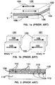
- a prior MRAM memory element 101 includes a data layer 102 and a reference layer 104 that are separated by a thin tunnel barrier layer 106.
- the tunnel barrier layer 106 is a thin film with a thickness that is less than about 2.0 nm.
- the barrier layer 106 is an electrically non-conductive dielectric material such as aluminum oxide (Al 2 O 3 ), for example.
- the tunnel barrier layer 106 is an insulator through which a tunneling current passes. The magnitude of the tunneling current and the quality of the tunneling current are greatly influenced by the quality of the insulator used for the tunnel barrier layer 106 . As a voltage that is applied across the tunnel barrier layer 106 is increased, the tunneling current increases in a nonlinear fashion.
- the reference layer 104 has a pinned orientation of magnetization 108 , that is, the pinned orientation of magnetization 108 is fixed in a predetermined direction and does not rotate in response to an external magnetic field.
- the data layer 102 has an alterable orientation of magnetization 103 that can rotate between two orientations in response to an external magnetic field.
- the alterable orientation of magnetization 103 is typically aligned with an easy axis E of the data layer 102.
- the data layer 102 and the reference layer 104 serve as electrodes of a tunnel junction device which allow the state of the bit stored in the data layer 102 to be sensed by measuring a resistance across the data layer 102 and the reference layer 104 or a by measuring a magnitude of the aforementioned tunneling current.
- the reference layer 104 is shown positioned below the tunnel barrier layer 106 , the actual position of the data layer 102 and the reference layer 104 will depend on the order in which they are formed in a process for fabricating the magnetic memory cell 101. Accordingly, the data layer 102 can be formed first and the tunnel barrier layer 106 formed on top of the data layer 102.
- the tunnel barrier layer 106 of a tunnel junction device is flat and has a uniform thickness T throughout its cross-sectional area.
- an ideal tunnel barrier layer 106 would be made from a dielectric material that is homogenous.
- One of the criteria for an ideal tunnel barrier layer 106 is that it have a high breakdown voltage. That is, the voltage at which the dielectric material of the tunnel barrier layer 106 breaks down and the tunnel barrier layer 106 acts as a shorted resistance.
- tunnel junction devices such as the prior memory cells 101
- defects in the tunnel barrier layer 106 result in a low breakdown voltage or an electrical short. Those defects include pin holes, bubbles, surface irregularities, metal inclusions, and non-uniformity of thickness in the tunnel barrier layer 106, just to name a few.
- a material for the tunnel barrier layer 106 is formed or deposited on a supporting layer 110 that can be the reference layer 106, the data layer 102, or another layer of a magnetic field sensitive memory cell, for example.
- the material for the tunnel barrier layer 106 can be aluminum (Al).
- the material is then exposed to oxygen (O 2 ) and is oxidized to form aluminum oxide (Al 2 O 3 ).
- the prior oxidation process doesn't uniformly oxidize all of the aluminum atoms and as a result there remains un-oxidized aluminum atoms 111 that form metal inclusion defects in the tunnel barrier layer 106.
- a portion of the oxygen atoms 112 remain un-reacted with the material 111 for the tunnel barrier layer 106 (i.e the aluminum); however, those un-reacted oxygen atoms 112 remain incorporated in the tunnel barrier layer 106.
- some of the oxygen atoms 112 react with and oxidize a portion of a material 113 for the supporting layer 110.
- oxidized atoms 113 at an interface between the tunnel barrier layer 106 and the supporting layer 110 create a defect that lowers the break down voltage of the tunnel barrier layer 106 .
- Prior methods for depositing or forming the tunnel barrier layer 106 such as RF-sputtering, plasma oxidation, or UV-ozone oxidation ultimately leave some defects in the tunnel barrier layer 106 that result in a poor tunneling barrier with weak points therein that cause shorting or a low breakdown voltage. Moreover, the existence of those defects makes it necessary to form a thicker nitride/oxide layer for the tunnel barrier layer 106. Conversely, if the dielectric material is a really good dielectric, then the thickness of the tunnel barrier layer 106 can be reduced. A thinner tunnel barrier layer 106 also helps in improving uniformity across an entire wafer that carries multiple tunnel junction devices. A thinner tunnel barrier layer 106 also lowers absolute resistance of the tunnel junction which can be important in some applications.
- the method of the present invention address the aforementioned needs for a uniform tunnel barrier layer by exposing a tunnel barrier layer of a tunnel junction device to ultra-violet light.
- Oxygen or another reactant, such as nitrogen, disposed in the tunnel barrier layer from a previous processing step is activated by the ultra-violet radiation and heals out defects in the tunnel barrier layer.
- the ultra-violet light can be from an ultra-violet light source that is incorporated into an existing piece of processing equipment.
- the tunnel barrier layer can be formed first and then irradiated by the ultra-violet light or the tunnel barrier layer can be irradiated by the ultra-violet light during the formation of the tunnel barrier layer.
- Either process can occur in situ so that potential contamination of the tunnel barrier layer or other layers of thin film in a MRAM stack or other tunnel junction device are reduced or eliminated.
- One advantage of the method of the present invention is that it may be combined with an oxidation or a nitridation process so that the irradiation with the ultra-violet light can occur during or after the oxidation or nitridation and the method can be easily integrated with existing oxidation or nitridation processing equipment.
- heat from a heat source is applied to the tunnel barrier layer of the tunnel junction device to further increase the activation process. As a result, more defects are removed and processing time for the activation can be reduced.
- the heating can occur before, during, or after the irradiation with the ultra-violet light.
- FIG. 1a is a profile view of a prior magnetic memory element.
- FIG. 1b is a schematic depicting data storage in the prior magnetic memory element of FIG. 1a.
- FIG. 2 is a cross-sectional view depicting defects in a prior tunnel barrier layer of a prior tunnel junction device.
- FIG. 3 is a cross-sectional view depicting a plurality of thin film layers of a tunnel junction device including a precursor layer according to the present invention.
- FIG. 4 is a cross-sectional view depicting formation of a tunnel barrier layer on a precursor layer according to the present invention.
- FIGS. 5a and 5b are cross-sectional views depicting irradiating a tunnel barrier layer with ultra-violet light and activation of a reactant according to the present invention.
- FIG. 5c is a cross-sectional view depicting completed activation of a reactant in the tunnel barrier layer by the ultra-violet light according to the present invention.
- FIGS. 6a and 6b are cross-sectional views depicting the application of heat to the tunnel barrier layer to increase an activation rate of a reactant according to the present invention.
- FIG. 7 is a cross-sectional view depicting a tunnel barrier layer that is formed on a precursor layer of a tunnel junction device according to the present invention.
- the present invention is embodied in a method of treating a tunnel barrier layer of a tunnel junction device using ultra-violet light to activate a reactant disposed in the tunnel barrier layer so that the reactant reacts with a material of the tunnel barrier layer resulting in an increase in a uniformity of oxidation or nitridation of the tunnel barrier layer.
- the method of the present invention is applicable to treating defects in a tunnel barrier layer of a tunnel junction device, the present invention is not limited to the treatment of tunnel barrier layers and is applicable to any dielectric layer of a tunnel junction device in which is desirable to heal out defects in the dielectric layer.
- a tunnel barrier layer 6 is formed on a precursor layer 4 of a tunnel junction device 10 .
- the precursor layer 4 can be any of the layers of thin film materials that comprise the tunnel junction device 10 including but not limited to one or more layers of a data layer (also called a storage layer or free layer) or one or more layers of a reference layer (also called a pinned layer) of a magnetic field sensitive memory device.
- the tunnel barrier layer 6 and the precursor layer 4 can be one of several layers of a TMR memory cell.
- the tunnel junction device 10 can include other layers such as a layer 2 that supports the precursor layer 4 and a layer 8 .
- the layer 8 can be a substrate such as a silicon (Si) wafer, for example.
- the layers 8 , 2 , and 4 of the tunnel junction device 10 are formed in an ordered sequence as indicated by a dashed arrow p such that layer 8 precedes layer 2 and layer 2 precedes layer 4 in the ordered sequence p . Accordingly, the precursor layer 4 is that layer which precedes the tunnel barrier layer 6 in the ordered sequence p . Subsequent process steps (not shown) that occur after the formation of the tunnel barrier layer 6 in the ordered sequence p are required to complete the formation of the tunnel junction device 10.
- a magnetic field sensitive memory device such as the tunnel junction device 10 can include a plurality of layers of thin film materials, for purposes of illustration, the tunnel junction device 10 is shown as including the precursor layer 4 , and the tunnel barrier layer 6 , but is not to be construed as being limited to those layers only.
- the tunnel barrier layer 6 is formed on the precursor layer 4 of the tunnel junction device 10.
- Microelectronics processing techniques that are commonly used for forming thin film materials can be used to form the tunnel barrier layer 6.
- a deposition or a sputtering process can be used to deposit a material for the tunnel barrier layer 6 on a surface 5 of the precursor layer 4.
- Suitable materials for the tunnel barrier layer 6 include but are not limited to aluminum (Al), magnesium (Mg), boron (B), and tantalum (Ta).
- the process for forming the tunnel barrier layer 6 can be a process including but not limited to RF sputtering, DC sputtering, evaporation, plasma assisted deposition, chemical vapor deposition (CVD), physical vapor deposition (PVD), plasma enhanced chemical vapor deposition (PECVD), molecular beam epitaxy (MBE), and metalorganic chemical vapor deposition (MOCVD).
- the oxide or nitride material for the tunnel barrier layer 6 can also be reactively sputtered from an oxide or a nitride target material. For instance, if the material to be deposited is aluminum oxide, then the target material can be Al 2 O 3 . However, after the sputtering process is over, the defects in the tunnel barrier layer 6 still need to be healed out.
- the tunnel barrier layer 6 is then transformed into an electrically non-conductive material (i.e. a dielectric material) using an oxidation process for the formation of an oxide, or a nitridation process for the formation of a nitride.
- a reactant 12 such as atoms of oxygen (O 2 ) or atoms of nitrogen (N 2 ) are introduced 20 into the material of the tunnel barrier layer 6.
- Some of the reactant 12 chemically reacts with a material of the tunnel barrier layer 6 to form an electrically non-conductive material such as an oxide in the case of oxygen (O 2 ) or a nitride in the case of nitrogen (N 2 ).
- the reactant 12 chemically reacts with the material 11 of the tunnel barrier layer 6 . Consequently, some of the reactant remains in the material of the tunnel barrier layer 6 in an un-reacted state (see reference numeral 12 ). Similarly, some of the material for the tunnel barrier layer 6 also remains un-reacted (see reference numeral 11 ). For instance, atoms of aluminum can remain un-reacted. Additionally, some of the reactant 12 reacts with a material (see reference numeral 13 ) for the precursor layer 4 in a region proximate the surface 5 of the precursor layer 4 .
- the reactant 12 that has reacted with the material 13 is not reacted with the material 11 of the tunnel barrier layer 6, that reactant is also in an un-reacted state because it has not reacted with the intended target material 11 of the tunnel barrier layer 6 and because there are free atoms 11 of the target material within the tunnel barrier layer 6 that are available to react with the reactant 12.
- the reactant 12 that remains un-reacted can give rise to the aforementioned defects in the tunnel barrier layer 6 that can reduce the break down voltage and/or result in non-uniformity in the tunnel barrier layer 6.
- ultra-violet light 30 from a light source 32 i.e. a light source that emits radiation in the ultra-violet spectrum
- a light source 32 i.e. a light source that emits radiation in the ultra-violet spectrum
- a portion of the ultra-violet light 30 is incident on the reactant 12 that is disposed in the tunnel barrier layer 6 as a result of the process used to transform the tunnel barrier layer 6 into an electrically non-conductive material.
- the ultra-violet light 30 activates the reactant 12 so that it chemically reacts with the material 11 of the tunnel barrier layer 6 and transforms the material 11 into the electrically non-conductive material.
- the energy of the ultra-violet light 30 activates the reactant 12 so that the reactant 12 chemically reacts with the free atoms of the material 11 of the tunnel barrier layer 6 to form the electrically non-conductive material.
- the desired electrically non-conductive material is aluminum oxide (Al 2 O 3 ).
- the irradiation operates to activate the oxygen atoms by transferring energy from the ultra-violet light 30 to the oxygen atoms thereby providing the energy necessary to complete the chemical reaction of the oxygen atoms and the aluminum atoms to form aluminum oxide.
- the source 32 for the ultra-violet light 30 can be a commercially available UV light source including but not limited to a cold cathode UV grid lamp or a hot cathode UV spiral lamp, for example.
- the wavelength of the ultra-violet light 30 will be application dependent. Typically, light having a wavelength (in nanometers) between about 4 nm and about 400 nm is considered to be ultra-violet radiation. Near UV is in a range of about 400 nm to about 300 nm, Far UV is in a range from about 300 nm to about 200 nm, and anything below about 200 nm is considered to be Extreme UV.
- the wavelength for the ultra-violet light 30 is in a range from about 200 nm to about 400 nm.
- FIG. 5b a portion of the ultra-violet light 30 (see dashed arrows) is incident on the reactant 12, the reactant 12 is activated (see dashed arrows a ) , and the reactant 12 chemically reacts with the material 11 of the tunnel barrier layer 6 .
- FIG. 5c a chemical bonding of the reactant 12 with the with the material 11 results in the forming of the electrically non-conductive material.
- a chemical bond between the material 13 and the reactant 12 is broken (by the ultra-violet radiation 30 ) so that the reactant 12 is free to bond with the material 11 .
- oxidation process can be a process including but not limited to plasma oxidation, natural oxidation, room temperature natural oxidation (i.e. at about 25 °C), and UV-ozone oxidation.
- UV-ozone oxidation is not to be confused with irradiation of the tunnel barrier layer 6 with the ultra-violet light 30 .
- UV-ozone oxidation is a separate process wherein oxygen (O 2 ) gas is exposed to ultra-violet light to convert the oxygen gas to ozone (O 3 ).
- the ozone is then introduced into the tunnel barrier layer 6 .
- the ozone increases a reaction rate with the material 11 of the tunnel barrier layer 6 because ozone (O 3 ) is highly reactive and is more reactive than O 2 with the material 11 of the tunnel barrier layer 6 .
- the reactant 12 can be a material including but not limited to oxygen (O 2 ), ozone (O 3 ), or nitrogen (N 2 ).
- the irradiating of the tunnel barrier layer 6 with the ultra-violet light can be continued for a predetermined amount of time until a desired property of the tunnel barrier layer 6 is obtained.
- the desired property can be a property including but not limited to a predetermined defect density in the tunnel barrier layer 6 , a predetermined breakdown voltage of the tunnel barrier layer 6 , a change in a crystal structure of the tunnel barrier layer 6 , and a change in a texture of a grain orientation of tunnel barrier layer 6 .
- the defect density can be the number of metal inclusions (i.e. defects) per unit of area or unit of volume of the tunnel barrier layer 6 .
- the texture of some grain orientations may grow as a result of irradiation with the ultra-violet 30 .
- the crystal structure of the tunnel barrier layer 6 can change from amorphous to crystalline as a result of irradiation with the ultra-violet 30 . Verification of the efficacy of some of the aforementioned desired properties of the tunnel barrier layer 6 can be accomplished by structural characterization using a tool such as a Transmission Electron Microscope (TEM), for example.
- TEM Transmission Electron Microscope
- the ultra violet light 30 can be generated by an ultra-violet light source 32 that is positioned in a chamber (not shown) in which some or all of the processing of the tunnel junction device 10 takes place.
- the ultra-violet light source 32 can also irradiate the tunnel barrier layer 6 through a window that is optically transparent to a wavelength of the ultra violet light 30 .
- the tunnel barrier layer 6 can be heated H before, during, or after the irradiating process to increase an activation rate of the reactant 12 with the material 11 of the tunnel barrier layer 6 .
- the heating H speeds up the activation process and removes more defects from the tunnel barrier layer 6 .
- the tunnel barrier layer 6 is heated H to increase the activation rate.
- the reactant 12 is activated (see dashed arrows a ) and reacts with the material 11 of the tunnel barrier layer 6.
- a variety of methods that are well known in the microelectronics art can be used to heat H the tunnel barrier layer 6.
- the substrate 8 (see FIG. 3 ) can be heated H by placing the substrate 8 on a vacuum chuck, stage, sample platform, or the like that contains a heat source or is in thermal communication with a heat source.
- a heat source such as a quartz infrared heat lamp, a resistance heater, or a metal ribbon radiant heater can be used to heat the substrate 8 or the tunnel barrier layer 6 .
- the heating of the tunnel barrier layer 6 can occur during or after the irradiation with the ultra-violet light 30 .
- an electrically non-conductive tunnel barrier layer 6 is formed 20 directly on the surface 5 of the precursor layer 4. That is, the material 11 for the tunnel barrier layer 6 is already a dielectric material prior to it being formed on the precursor layer 4.
- a process including but not limited to a sputtering process and a reactive sputtering process can be used to form the electrically non-conductive tunnel barrier layer 6.
- a target material for the sputtering process and the reactive sputtering process includes but is not limited to an oxide material and a nitride material.
- a sputtering target such as an aluminum oxide (Al 2 O 3 ), aluminum nitride (AlN x ), magnesium oxide (MgO), or tantalum oxide (TaO x ) can be the source material for the electrically non-conductive tunnel barrier layer 6.
- Al 2 O 3 aluminum oxide
- AlN x aluminum nitride
- MgO magnesium oxide
- TaO x tantalum oxide
- the electrically non-conductive tunnel barrier layer 6 is irradiated with the ultra-violet light 30 from an ultra-violet light source 32 and activates a reactant 12 to react with a material 11 of electrically non-conductive tunnel barrier layer 6 as was described above in reference to FIGS. 4, 5a, 5b, and 5c.
- the electrically non-conductive tunnel barrier layer 6 can be heated H during or after the irradiating to increase an activation rate of the reactant 12 with the material 11 of the electrically non-conductive tunnel barrier layer 6 as was described above in reference to FIGS. 6a and 6b .
- a tunnel barrier layer 6 is previously formed on a precursor layer 4 of a tunnel junction device 10 and contains the defects (11, 12, 13). That is, the tunnel barrier layer 6 has already been deposited, sputtered, or otherwise formed on the precursor layer 4 and is already an electrically non-conductive material.
- the tunnel barrier layer 6 is irradiated with ultra-violet light 30 and the ultra-violet light 30 is incident on a reactant 12 disposed in the tunnel barrier layer 6. As was described above, the ultra-violet light 30 activates the reactant 12 to react with a material 11 of the tunnel barrier layer 6 (see FIGS. 5a through 5c ) to transform the material 11 into the electrically non-conductive material.
- the tunnel barrier layer 6 is already an electrically non-conductive material; however, the irradiation serves to react un-reacted free atoms of the reactant 12 with the material 11 to increase uniformity, homogeneity, and breakdown voltage of the tunnel barrier layer 6.
- the reactant 12 can be a material including but not limited to oxygen (O 2 ), ozone (O 3 ), or nitrogen (N).
- the tunnel barrier layer 6 can be heated H during or after the irradiating to increase the activation rate as was described above in reference to FIGS. 6a and 6b.
- the irradiation with the ultra-violet light 30 and the heating H can occur in situ with other microelectronic processes for forming the tunnel junction device 10 and can occur during or after the formation of the tunnel barrier layer 6 .
Landscapes
- Engineering & Computer Science (AREA)
- Chemical & Material Sciences (AREA)
- Nanotechnology (AREA)
- Physics & Mathematics (AREA)
- Crystallography & Structural Chemistry (AREA)
- General Physics & Mathematics (AREA)
- Manufacturing & Machinery (AREA)
- Condensed Matter Physics & Semiconductors (AREA)
- Power Engineering (AREA)
- Spectroscopy & Molecular Physics (AREA)
- Computer Hardware Design (AREA)
- Hall/Mr Elements (AREA)
- Semiconductor Memories (AREA)
- Mram Or Spin Memory Techniques (AREA)
- Junction Field-Effect Transistors (AREA)
Abstract
Description
Claims (11)
- A method of treating a tunnel barrier layer 6 formed on a precursor layer 4 of a tunnel junction device 10, comprising:wherein the ultra-violet light 30 is operative to activate a the reactant 12 so that the reactant 12 reacts with a material 11 of the tunnel barrier layer 6 and transforms the material 11 into an electrically non-conductive material.irradiating the tunnel barrier layer 6 with ultra-violet light 30, the ultra-violet light 30 being incident on a reactant 12 disposed in the tunnel barrier layer 6,
- A method as claimed in claim 1 and further comprising:heating H the tunnel barrier layer 6 to increase an activate rate of the reactant 12 with the material 11 of the tunnel barrier layer 6, the heating H occurring before, during or after the irradiating step.
- A method as claimed in claim 1 or 2, wherein the material 11 for the tunnel barrier layer 6 comprises aluminium, magnesium, boron, or tantalum.
- A method as claimed in any preceding claim, wherein the reactant 12 comprises oxygen, ozone or nitrogen.
- A method as claimed in any preceding claim and further comprising continuing the irradiating with the ultra-violet light 30 for a predetermined time until a desired property of the tunnel barrier layer 6 is obtained.
- A method as claimed in claim 5, wherein the desired property of the tunnel barrier layer 6 is a predetermined defect density in the tunnel barrier layer 6, a predetermined breakdown voltage of the tunnel barrier layer 6, a change in a crystal structure of the tunnel barrier layer 6, or a change in a texture of a grain orientation of tunnel barrier layer 6.
- A method as claimed in any preceding claim and further comprising:forming said tunnel barrier layer 6 on the precursor layer 4 of the tunnel junction device 10 wherein said tunnel barrier layer is electrically non-conductive.
- A method as claimed in claim 7, wherein the forming comprises RF sputtering, DC sputtering, evaporation, plasma assisted deposition, chemical vapor deposition, physical vapor deposition, plasma enhanced chemical vapor deposition, molecular beam epitaxy, or metalorganic chemical vapor deposition.
- A method as claimed in claim 8, wherein a target material for the sputtering process is an oxide material or a nitride material.
- A method as claimed in any preceding claim and further comprising:transforming said tunnel barrier layer 6 into an electrically non-conductive material by means of an oxidation process or a nitridation process.
- A method as claimed in claim 10, wherein the oxidation process comprises plasma oxidation, natural oxidation, room temperature natural oxidation, or UV-ozone oxidation.
Applications Claiming Priority (2)
| Application Number | Priority Date | Filing Date | Title |
|---|---|---|---|
| US282577 | 2002-10-29 | ||
| US10/282,577 US20040082081A1 (en) | 2002-10-29 | 2002-10-29 | Ultra-violet treatment for a tunnel barrier layer in a tunnel junction device |
Publications (2)
| Publication Number | Publication Date |
|---|---|
| EP1416530A2 true EP1416530A2 (en) | 2004-05-06 |
| EP1416530A3 EP1416530A3 (en) | 2009-04-29 |
Family
ID=32093477
Family Applications (1)
| Application Number | Title | Priority Date | Filing Date |
|---|---|---|---|
| EP03256454A Withdrawn EP1416530A3 (en) | 2002-10-29 | 2003-10-13 | Treatment of a tunnel barrier layer |
Country Status (5)
| Country | Link |
|---|---|
| US (1) | US20040082081A1 (en) |
| EP (1) | EP1416530A3 (en) |
| JP (1) | JP2004153257A (en) |
| CN (1) | CN1523648A (en) |
| TW (1) | TW200406939A (en) |
Cited By (1)
| Publication number | Priority date | Publication date | Assignee | Title |
|---|---|---|---|---|
| CN100359566C (en) * | 2004-08-26 | 2008-01-02 | 日立环球储存科技荷兰有限公司 | Reactive sputter deposition method for fabricating magnesium oxide tunnel barriers in magnetic tunnel junctions |
Families Citing this family (7)
| Publication number | Priority date | Publication date | Assignee | Title |
|---|---|---|---|---|
| US6771473B2 (en) * | 2001-01-22 | 2004-08-03 | Matsushita Electric Industrial Co., Ltd. | Magnetoresistive element and method for producing the same |
| SG157992A1 (en) * | 2008-07-01 | 2010-01-29 | Showa Denko Hd Singapore Pte L | Improvements in and relating to mram |
| TWI384493B (en) * | 2008-11-24 | 2013-02-01 | Hung Tao Peng | Micro - Atomic Energy Power Generators for Military and Civilian Generations and Their Generating Methods |
| US8227896B2 (en) * | 2009-12-11 | 2012-07-24 | International Business Machines Corporation | Resistive switching in nitrogen-doped MgO |
| US10565942B2 (en) * | 2014-07-29 | 2020-02-18 | Hewlett-Packard Development Company, L.P. | Display device |
| US10210920B1 (en) | 2018-03-27 | 2019-02-19 | Qualcomm Incorporated | Magnetic tunnel junction (MTJ) devices with varied breakdown voltages in different memory arrays fabricated in a same semiconductor die to facilitate different memory applications |
| CN110581215B (en) * | 2018-06-07 | 2022-10-28 | 联华电子股份有限公司 | Method of forming a magnetoresistive random access memory cell |
Family Cites Families (1)
| Publication number | Priority date | Publication date | Assignee | Title |
|---|---|---|---|---|
| DE19938215A1 (en) * | 1999-08-12 | 2001-02-22 | Forschungszentrum Juelich Gmbh | Process for producing a magnetic tunnel contact and magnetic tunnel contact |
-
2002
- 2002-10-29 US US10/282,577 patent/US20040082081A1/en not_active Abandoned
-
2003
- 2003-05-01 TW TW092112030A patent/TW200406939A/en unknown
- 2003-08-29 CN CNA031556353A patent/CN1523648A/en active Pending
- 2003-10-07 JP JP2003347735A patent/JP2004153257A/en not_active Withdrawn
- 2003-10-13 EP EP03256454A patent/EP1416530A3/en not_active Withdrawn
Cited By (1)
| Publication number | Priority date | Publication date | Assignee | Title |
|---|---|---|---|---|
| CN100359566C (en) * | 2004-08-26 | 2008-01-02 | 日立环球储存科技荷兰有限公司 | Reactive sputter deposition method for fabricating magnesium oxide tunnel barriers in magnetic tunnel junctions |
Also Published As
| Publication number | Publication date |
|---|---|
| TW200406939A (en) | 2004-05-01 |
| EP1416530A3 (en) | 2009-04-29 |
| CN1523648A (en) | 2004-08-25 |
| JP2004153257A (en) | 2004-05-27 |
| US20040082081A1 (en) | 2004-04-29 |
Similar Documents
| Publication | Publication Date | Title |
|---|---|---|
| US6828260B2 (en) | Ultra-violet treatment of a tunnel barrier layer through an overlayer a tunnel junction device | |
| US11245069B2 (en) | Methods for forming structures with desired crystallinity for MRAM applications | |
| US6710986B1 (en) | Tunneling magnetoresistive head and a process of tunneling magnetoresistive head | |
| US20120043518A1 (en) | Variable resistance memory element and fabrication methods | |
| RU2550464C2 (en) | Device and method for substrate fast heating and cooling and application of coating thereon in vacuum | |
| US20030036238A1 (en) | Process for direct integration of a thin-film silicon p-n junction diode with a magnetic tunnel junction | |
| JP5320100B2 (en) | Method for enhancing hydrogenation of oxide encapsulated materials | |
| JP4708793B2 (en) | CU2S MOCVD formation | |
| US9368177B2 (en) | Magnetic resistance structure, method of manufacturing the magnetic resistance structure, and electronic device including the magnetic resistance structure | |
| RU2367057C2 (en) | Method of forming structures of magnetic tunnel barriers for magnetoresistive random access magnetic memory and structure of magnetic tunnel barrier for magnetoresistive random access magnetic memory (versions) | |
| EP1416530A2 (en) | Treatment of a tunnel barrier layer | |
| KR20040043048A (en) | Magnetic tunnel junction device and Fabricating method thereof | |
| US20050270821A1 (en) | Semiconductor device and manufacturing method for same | |
| JP4630856B2 (en) | Method for manufacturing magnetoresistive element | |
| US10038138B1 (en) | High temperature volatilization of sidewall materials from patterned magnetic tunnel junctions | |
| TWI903030B (en) | Semiconductor device and method for producing the same | |
| HK1066921A (en) | Ultra-violet treatment for a tunnel barrier layer in a tunnel junction device | |
| HK1065642A (en) | Ultra-violet treatment of a tunnel barrier layer through an overlayer in a tunnel junction device | |
| KR20020008475A (en) | Manufacturing Process of Tunneling Magnetoresistive Devices | |
| KR100543265B1 (en) | Tunneling magnetoresistive element and manufacturing method thereof | |
| JP3887367B2 (en) | Method and apparatus for manufacturing element having tunnel junction | |
| JP3799438B2 (en) | Manufacturing method of semiconductor oxide film | |
| KR100798696B1 (en) | PMCM element having a solid electrolyte composed of silver-saturated thin-film thin film and method for manufacturing same | |
| Zafar et al. | A low-tech solution to process entire metal/molecule heterostructure stacks into vertical nanopillar electronic devices | |
| CN121357895A (en) | A high-density magnetic memory driven by spin-orbit torque and its fabrication method |
Legal Events
| Date | Code | Title | Description |
|---|---|---|---|
| PUAI | Public reference made under article 153(3) epc to a published international application that has entered the european phase |
Free format text: ORIGINAL CODE: 0009012 |
|
| AK | Designated contracting states |
Kind code of ref document: A2 Designated state(s): AT BE BG CH CY CZ DE DK EE ES FI FR GB GR HU IE IT LI LU MC NL PT RO SE SI SK TR |
|
| AX | Request for extension of the european patent |
Extension state: AL LT LV MK |
|
| PUAL | Search report despatched |
Free format text: ORIGINAL CODE: 0009013 |
|
| AK | Designated contracting states |
Kind code of ref document: A3 Designated state(s): AT BE BG CH CY CZ DE DK EE ES FI FR GB GR HU IE IT LI LU MC NL PT RO SE SI SK TR |
|
| AX | Request for extension of the european patent |
Extension state: AL LT LV MK |
|
| RIC1 | Information provided on ipc code assigned before grant |
Ipc: H01F 41/30 20060101ALI20090326BHEP Ipc: H01F 10/32 20060101ALI20090326BHEP Ipc: G11B 5/33 20060101ALI20090326BHEP Ipc: G01R 33/09 20060101ALI20090326BHEP Ipc: G11C 11/16 20060101ALI20090326BHEP Ipc: H01L 21/8246 20060101AFI20040310BHEP |
|
| AKX | Designation fees paid | ||
| REG | Reference to a national code |
Ref country code: DE Ref legal event code: 8566 |
|
| STAA | Information on the status of an ep patent application or granted ep patent |
Free format text: STATUS: THE APPLICATION IS DEEMED TO BE WITHDRAWN |
|
| 18D | Application deemed to be withdrawn |
Effective date: 20091030 |