EP1411637A2 - Programmable logic devices with silicon-germanium circuitry and associated methods - Google Patents
Programmable logic devices with silicon-germanium circuitry and associated methods Download PDFInfo
- Publication number
- EP1411637A2 EP1411637A2 EP03023559A EP03023559A EP1411637A2 EP 1411637 A2 EP1411637 A2 EP 1411637A2 EP 03023559 A EP03023559 A EP 03023559A EP 03023559 A EP03023559 A EP 03023559A EP 1411637 A2 EP1411637 A2 EP 1411637A2
- Authority
- EP
- European Patent Office
- Prior art keywords
- silicon
- circuitry
- layer
- programmable logic
- pld
- Prior art date
- Legal status (The legal status is an assumption and is not a legal conclusion. Google has not performed a legal analysis and makes no representation as to the accuracy of the status listed.)
- Withdrawn
Links
Images




Classifications
-
- H—ELECTRICITY
- H03—ELECTRONIC CIRCUITRY
- H03K—PULSE TECHNIQUE
- H03K19/00—Logic circuits, i.e. having at least two inputs acting on one output; Inverting circuits
- H03K19/02—Logic circuits, i.e. having at least two inputs acting on one output; Inverting circuits using specified components
- H03K19/173—Logic circuits, i.e. having at least two inputs acting on one output; Inverting circuits using specified components using elementary logic circuits as components
-
- H—ELECTRICITY
- H10—SEMICONDUCTOR DEVICES; ELECTRIC SOLID-STATE DEVICES NOT OTHERWISE PROVIDED FOR
- H10D—INORGANIC ELECTRIC SEMICONDUCTOR DEVICES
- H10D84/00—Integrated devices formed in or on semiconductor substrates that comprise only semiconducting layers, e.g. on Si wafers or on GaAs-on-Si wafers
- H10D84/90—Masterslice integrated circuits
Definitions
- This patent application relates generally to programmable logic devices (PLDs) and, more particularly, to PLDs that include circuitry fabricated using silicon-germanium (SiGe).
- PLDs programmable logic devices
- SiGe silicon-germanium
- a typical PLD uses a memory to program the logic circuitry within the PLD.
- the memory typically resides on the same silicon die and. in the same silicon substrate as do the logic circuitry and other circuitry within the PLD.
- the memory may store a large number of bits. Consequently, the memory typically consumes a relatively large and substantial area of the silicon die.
- the area that the memory consumes reduces the area available to the other circuitry within the PLD, such as the logic circuitry.
- the overall capacity of the PLD in decreases.
- a PLD according to the invention includes programmable electronic circuitry fabricated in a semiconductor substrate (such as a silicon substrate).
- the PLD also includes memory circuitry coupled to the programmable electronic circuitry.
- the memory circuitry is fabricated using SiGe.
- a data-processing system in another embodiment, includes a PLD.
- the PLD contains programmable logic circuitry configured to allow programming the functionality of the programmable logic device (PLD) in response to programming information.
- the programmable logic circuitry further configured to reside in a semiconductor substrate (such as a silicon substrate).
- the PLD also includes a memory circuitry fabricated using silicon-germanium-based circuitry. The memory circuitry provides the programming information to the programmable logic circuitry.
- a PLD in a third embodiment, includes a first block of circuitry and a second block of circuitry.
- the first block of circuitry includes programmable logic circuitry.
- the second block of circuitry is fabricated using silicon-germanium and couples to the first block of circuitry.
- the first block of circuitry includes programmable logic circuitry (e.g., look-up tables, configurable logic circuitry, etc.).
- the second block of circuitry may include memory circuitry used to program the PLD, redundancy circuitry (circuitry that bypasses, removes, or detects defective circuits within the PLD detected during a test procedure) or, generally, any other circuitry not within the data path of the PLD (i.e., any circuitry outside the PLD's data path).
- a PLD in a fourth embodiment, includes a plurality of programmable logic blocks fabricated in a semiconductor substrate, first and second sets of programmable interconnects, and a plurality of memory elements.
- the first and second sets of programmable interconnects are disposed in a first dimension and a second dimension within the PLD, respectively.
- the plurality of memory elements couple to the plurality of programmable logic blocks and to the first and second sets of programmable interconnects. At least one element in the plurality of memory elements is fabricated in at least one layer disposed above the semiconductor substrate.
- a method according to the invention for fabricating a PLD includes producing a programmable electronic circuit in a semiconductor (e.g., silicon) substrate. The method also includes fabricating a memory circuit using silicon-germanium. The memory circuit couples to the programmable electronic circuit.
- a semiconductor e.g., silicon
- a method according to the invention for fabricating a PLD includes fabricating a first block of circuitry within the PLD. The method further includes fabricating a second block of circuitry coupled to the first block of circuitry. The second block of circuitry is fabricated using silicon-germanium.
- the first block of circuitry includes programmable logic circuitry (e.g., look-up tables, configurable logic circuitry, etc.):
- the second block of circuitry may include memory circuitry used to program the PLD, redundancy circuitry (circuitry that bypasses, removes, or detects defective circuits within the PLD detected during a test procedure) or, generally, any circuitry not within the data path of the PLD (i.e., any circuitry outside the data path of the PLD).
- FIG. 1 shows an exemplary embodiment of a circuit arrangement that includes a PLD according to the invention.
- FIG. 2 illustrates a cross-section of a portion of an exemplary embodiment of a PLD wafer fabricated according to the invention.
- FIG. 3 depicts a cross-section of a portion of another exemplary embodiment of a PLD wafer fabricated according to the invention.
- FIG. 4 shows a more detailed cross-section of a portion of an exemplary embodiment of a partially processed PLD wafer processed according to the invention.
- FIG. 5 illustrates another cross-section of a portion of an exemplary embodiment of a PLD wafer further processed according to the invention.
- FIG. 6 depicts another cross-section of a portion of an exemplary embodiment of a PLD wafer further processed according to the invention.
- FIG. 7 shows a cross-section of a portion of an exemplary embodiment of a PLD wafer according to the invention, including a PMOS transistor and an NMOS transistor.
- FIG. 8 illustrates a cross-section of a portion of an exemplary embodiment of a PLD wafer that includes a SiGe resistor fabricated according to the invention.
- FIG. 9 shows a cross-section of a portion of an exemplary embodiment of a PLD wafer further processed according to the invention that includes contacts.
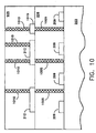
- FIG. 10 illustrates a cross-section of a portion of an alternative embodiment of a PLD wafer further processed according to the invention that includes contacts.
- FIG. 11 illustrates a block diagram of a circuit arrangement in an exemplary embodiment of a PLD according that includes a voltage translator.
- FIG. 12 depicts a portion of an exemplary embodiment of a PLD according to the invention that includes voltage translation or level-shifting.
- FIG. 13 shows a portion of another exemplary embodiment of a PLD according to the invention that includes voltage translation or level-shifting.
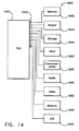
- FIG. 14 illustrates an exemplary embodiment of a data-processing system that includes a PLD according to the invention.
- This invention contemplates PLDs that include circuitry fabricated using silicon-germanium (SiGe), or SiGe-based circuitry.
- the SiGe-based circuitry resides above the semiconductor (e . g ., silicon) substrate that includes the logic circuitry.
- PLDs according to exemplary embodiments of the invention include SiGe-based circuitry deposited above an insulating layer above the semiconductor substrate where some of the PLD logic circuitry resides.
- the SiGe-based circuitry may use one or more layers of SiGe, one or more seed layers of silicon, and one or more layers of insulator or dielectric.
- One may use the SiGe-based circuitry to implement a memory used to program the PLD, redundancy circuitry (circuitry that bypasses, removes, or detects defective circuits within the PLD detected during a test procedure) or, generally, any other circuitry not within the data path of the PLD.
- redundancy circuitry circuitry that bypasses, removes, or detects defective circuits within the PLD detected during a test procedure
- any other circuitry not within the data path of the PLD rather than integrating the memory, redundancy circuitry, or other circuitry within the semiconductor substrate, one integrates such circuitry vertically with respect to the semiconductor substrate, i.e ., in the SiGe-based circuitry disposed or fabricated above the semiconductor substrate.
- memory 106 and redundancy circuitry 115 are merely examples of circuitry that is outside of the data path of the PLD. As noted above, one may generally integrate above the semiconductor substrate of the PLD any circuitry that resides or functions outside the PLD's data path.
- the SiGe-based circuitry fabricated in this manner solves the problems associated with conventional PLDs, described above. Use of the SiGe-based circuitry thus results in denser PLDs, with larger equivalent gate counts. Furthermore, the SiGe-based circuitry allows more efficient use of interconnect resources.
- FIG. 1 shows an exemplary embodiment of a circuit arrangement according to the invention.
- the circuit arrangement includes PLD 100 and programming data source 103.
- PLD 100 includes memory 106, programmable electronic circuitry 109, programmable interconnect 112, and redundancy circuitry 115.
- Programmable electronic circuitry 109 and programmable interconnect 112 allow one to configure the functionality of PLD 100 ( i . e ., to program PLD 100), as persons skilled in the art with the benefit of the description of the invention understand.
- Programming data source 103 may constitute an appropriate source of data used to program PLD 100. Programming data source 103 supplies data that configure the programmable electronic circuitry 109 via memory 106. Programming data source 103 may include a memory, such as random-access memory (RAM), dynamic RAM (DRAM), magnetic RAM (MRAM), read-only memory (ROM), programmable ROM (PROM), erasable PROM (EPROM), electrically erasable ROM (EEROM), disk, flash memory, and the like, as persons skilled in the art understand.
- RAM random-access memory
- DRAM dynamic RAM
- MRAM magnetic RAM
- ROM read-only memory
- PROM programmable ROM
- EPROM erasable PROM
- EEROM electrically erasable ROM
- Programmable electronic circuitry 109 may include a variety of configurable logic circuits, such as look-up-table (LUT) based logic circuits, memory, multiplexers, sequential logic, combinational logic, and the like.
- programmable electronic circuitry 109 may include a plurality of programmable logic blocks or circuitry (not shown explicitly). The logic blocks may be arranged as an array or grid (for example, a two-dimensional array of blocks) within PLD 100, as desired.
- Programmable interconnect 112 includes configurable coupling structures, for example, multiplexers and/or pass transistors. One may program or control the interconnect resources to provide a desired interconnection among various programmable or configurable circuits with PLD 100, such as other interconnect resources or programmable logic circuitry.
- programmable interconnect 112 may include programmable interconnects arranged in two dimensions ( e . g ., horizontally and vertically, or diagonally, and the like).
- one set of programmable interconnects may be arranged or disposed in a first dimension (e.g ., horizontally) of PLD 100, whereas a second set of programmable interconnects may be arranged or disposed in a second dimension of PLD 100 ( e.g. , vertically), as desired.
- Memory 106 couples to programmable electronic circuitry 109 and programmable interconnect 112.
- Memory 106 uses the programming data to configure the programmable interconnect 112 and programmable electronic circuitry 109 in a manner known in the art.
- the programming data may configure multiplexers, look-up tables, etc.
- memory 106 includes a plurality of static random-access memory (SRAM) elements implemented using SiGe-based circuitry.
- SRAM static random-access memory
- the SRAM elements provides low stand-by power consumption and fast operation.
- CAM content-addressable memory
- memory 106 may have a block or granular structure, as desired.
- memory 106 may include a memory block that comprises a desired number of memory elements (such as SRAM elements).
- memory 106 uses SiGe-based circuitry.
- redundancy circuitry 115 may also include SiGe-based circuitry.
- one may implement in SiGe any circuitry within PLD 100 that does not reside within the data path of PLD 100 ( i.e. , does not affect the processing speed of PLD 100 after one has programmed PLD 100).
- SiGe-based circuitry such as memory 106 and/or redundancy circuitry 115 resides above the semiconductor substrate within which programmable electronic circuitry 109, other parts of PLD 100 (including possibly some of programmable interconnect 112) reside. Put another way, one vertically integrates the SiGe-based circuitry with respect to the semiconductor substrate by fabricating on or above the semiconductor substrate various layers, such as SiGe layers.
- memory 106 may partly or entirely reside above the semiconductor substrate. In other words, one may fabricate one or more memory elements in memory 106 above the semiconductor substrate, as desired. In one exemplary embodiment, some of the memory elements reside in the semiconductor substrate, whereas other memory elements are fabricated above the semiconductor substrate (using at least one layer of dielectric, semiconductor, etc., as described in detail herein). In another embodiment, all of the memory elements are fabricated above the semiconductor substrate.
- CMOS complementary metal oxide semiconductor
- NMOS and PMOS p-type or n-type metal oxide semiconductor
- SOI silicon on insulator
- memory 106 does not reside in the same semiconductor substrate (such as a silicon substrate) that includes silicon-based circuitry for PLD 100. Instead, it resides in SiGe layer(s) fabricated above the semiconductor substrate of PLD 100 or, put another way, one integrates memory 106 vertically with respect to the semiconductor substrate of PLD 100.
- FIG. 2 depicts a cross-section of a portion of an exemplary embodiment of a PLD wafer fabricated according to the invention that includes SiGe-based circuitry fabricated above the semiconductor substrate of the PLD.
- the PLD shown in FIG. 2 includes a silicon substrate 203, an oxide layer 206 (combinations of oxide and nitride, or other dielectric or insulator materials, as desired), and SiGe-based circuitry 212.
- the PLD further includes insulation layer 207, insulation layer 208, interconnect layer 216, and interconnect layer 217.
- Silicon substrate 203 includes silicon-based circuitry 209, such as programmable electronic circuitry 109, and possibly some of programmable interconnect 112, etc.
- Oxide layer 206 resides above silicon substrate 203 and silicon-based circuitry 209.
- oxide layer 206 constitutes a low-temperature oxide (LTO) layer.
- SiGe-based circuitry 212 resides above oxide layer 206.
- SiGe-based circuitry 212 may include memory 106, redundancy circuitry 115, or other circuitry, as described above.
- SiGe-based circuitry 212 constitutes circuitry implemented in polycrystalline SiGe.
- a plurality of contacts 215 provide a coupling mechanism between silicon-based circuitry 209 and SiGe-based circuitry 212. Through contacts 215, silicon-based circuitry 209 and SiGe-based circuitry 212 may communicate and provide signals and power to each other. For example, memory 106 implemented in SiGe-based circuitry 212 may configure programmable electronic circuitry 109 implemented in silicon-based circuitry 209 by communicating appropriate programming information to it.
- Insulation layer 207 resides above SiGe-based circuitry 212 and oxide layer 206.
- Interconnect layer 216, disposed above insulation layer 207 includes one or more contacts or coupling mechanisms (e.g ., integrated-circuit metal traces).
- Insulation layer 208 resides above insulation layer 207.
- Interconnect layer 217 resides above insulation layer 208, and includes one or more contacts or coupling mechanisms ( e.g ., integrated-circuit metal traces).
- Insulation layer 207 and insulation layer 208 may constitute LTO, combinations of oxide and nitride, or other insulator or dielectric materials, as desired.
- Interconnect layer 216 and interconnect layer 217 are part of the PLD's interconnect resources. They provide coupling mechanisms among the various components or blocks of circuitry within the PLD.
- the interconnect resources of the PLD may include other elements (not shown explicitly in FIG. 2), such as vias, as persons of ordinary skill in the art with the benefit of the description of the invention understand.
- FIG. 3 illustrates a cross-section of a portion of another exemplary embodiment of a PLD wafer according to the invention that includes SiGe-based circuitry fabricated above the semiconductor substrate of the PLD.
- the PLD shown in FIG. 3 includes a silicon substrate 203, a plurality of oxide (or combinations of oxide and nitride, or other dielectric or insulator materials, as desired) layers or regions 206A-206C, vias 218, and metal layer 221.
- oxide layers 206A-206C constitute LTO layers.
- PLDs according to the invention may include more than one metal layer (or other interconnect layer, such as polysilicon), fabricated using oxide layers or other dielectric layers as insulators, as persons of ordinary skill in the art who have the benefit of the description of the invention understand.
- Silicon substrate 203 includes silicon-based circuitry 209, such as programmable electronic circuitry 109, programmable interconnect 112, etc.
- Oxide layer 206A resides above silicon substrate 203 and silicon-based circuitry 209.
- Oxide layer 206B resides above oxide layer 206A.
- SiGe-based circuitry 212 resides within or beneath oxide layer 206B, above oxide layer 206A.
- SiGe-based circuitry 212 may include memory 106, redundancy circuitry 115, or other circuitry, as described above.
- SiGe-based circuitry 212 constitutes circuitry implemented in polycrystalline SiGe.
- Oxide layer 206C resides above oxide layer 206B.
- Metal layer 221 in turn resides above oxide layer 206C.
- oxide layers 206B and 206C may be from the same layer of deposited material, as desired, as persons skilled in the art with the benefit of the description of the invention understand. Furthermore, one may fabricate oxide layers 206B and 206C such that they surround SiGe-based circuitry 212, as desired.
- a plurality of vias 218 provide a coupling mechanism between metal layer 221 and silicon-based circuitry 209.
- silicon-based circuitry 209 may provide signals and power to metal layer 221, and vice-versa.
- vias 218 may also use vias 218 as a coupling mechanism between metal layer 221 and SiGe-based circuitry 212, as desired.
- contacts (not shown explicitly) to provide a coupling mechanism between SiGe-based circuitry 212 and silicon-based circuitry 209, as desired.
- FIGS. 4-10 provide more details of illustrative fabrication processes for SiGe-based circuitry in PLDs according to the invention.
- a semiconductor wafer such as a silicon wafer
- substrate one first processes the substrate through a conventional semiconductor fabrication process, such as a PMOS, NMOS, or CMOS process.
- the conventional fabrication process produces silicon-based circuitry 209, as persons of ordinary skill in the art understand.
- the semiconductor fabrication process typically includes steps where one forms silicide on the gate polysilicon, and deposits a layer of oxide.
- the fabrication process typically includes a planarization step of the oxide layer, for example, by chemical-mechanical polishing (CMP).
- CMP chemical-mechanical polishing
- the CMP process produces a substantially planar surface of oxide layer 206.
- one may employ another technique for example, a conventionally known resist deposit and etch back process, as persons of ordinary skill in the art who have the benefit of the description of the invention understand.
- the planarization process seeks to produce a nearly planar surface of oxide layer 206 (or other oxide or dielectric layers, as desired).
- silicide because of its desirable low resistivity and self-aligning properties, one may use other gate materials (e.g ., polysilicon alone or a polycrystalline SiGe layer) and/or processing techniques, as persons skilled in the art with the benefit of the description of the invention understand.
- FIG. 4 shows a cross-section of a wafer processed according to the invention.
- FIG. 4 depicts silicon transistors in silicon substrate 203.
- the silicon transistors include source regions 408, drain regions 411, gates 415, and gate oxide regions 418.
- Isolation region oxide 405 separate and electrically isolate the silicon transistors from one another.
- Gates 415 reside beneath or within oxide layer 206.
- Oxide layer 206 may comprise an LTO region.
- One may use low-pressure (LP) chemical vapor deposition (CVD) or a plasma-enhanced low-pressure deposition process to fabricate oxide layer 206.
- LP low-pressure
- CVD chemical vapor deposition
- plasma-enhanced low-pressure deposition process As a result of planarization through CMP or a similar process, oxide layer 206 has a substantially planar upper surface.
- SiGe-based circuitry 212 includes thin-film transistors (TFT).
- TFT fabrication processes using polysilicon employ relatively high temperatures, e.g ., 1000 °C.
- the relatively high temperatures anneal the polysilicon film in the TFT to increase its grain size and to activate the dopants.
- the annealing process improves the operating electrical parameters (e . g ., increased carrier mobility, low leakage) of the resulting transistors.
- the high temperatures may cause redistribution of semiconductor dopants in the silicon-based circuitry 209 and, generally, in substrate 203.
- FIG. 5 illustrates a cross-section of a portion of an exemplary embodiment of a PLD wafer further processed according to the invention.
- Wafer fabrication proceeds with formation of SiGe above the semiconductor substrate.
- fabrication processes according to the invention use lower temperatures than conventional processes.
- one deposits a relatively thin seed layer of silicon 505 on oxide layer 206.
- One may deposit seed layer of silicon 505 at temperatures in the range of about 400 °C to about 600 °C and to a thickness in the range of about 10 ⁇ to about 100 ⁇ .
- a typical process in exemplary embodiments uses a temperature range of about 450 °C to about 550 °C to deposit a layer of about 10 ⁇ to about 50 ⁇ thick.
- Seed layer of silicon 505 facilitates depositing SiGe layer 510 (SiGe does not tend to deposit directly on silicon-dioxide).
- Depositing a typical SiGe layer 510 in illustrative embodiments uses a temperature range of about 450 °C to about 550 °C to produce a layer about 0.1 ⁇ to about 0.3 ⁇ thick.
- the thickness of SiGe layer 510 determines in part the electrical characteristics of the thin-film transistors formed in SiGe layer 510. Making SiGe layer 510 too thick or too thin results in transistors that tend to be hard to control.
- the deposited SiGe material may have amorphous or polycrystalline form.
- one vertically integrates the SiGe-based circuitry with respect to the semiconductor substrate by depositing on the semiconductor substrate various layers of semiconductor fabrication materials, such as semiconductor (e.g ., SiGe), insulator or dielectric ( e.g ., LTO), and interconnect (e.g ., metal layer, vias).
- semiconductor e.g ., SiGe
- insulator or dielectric e.g ., LTO
- interconnect e.g ., metal layer, vias
- exemplary embodiments according to the invention use polycrystalline SiGe. Also as noted above, one deposits SiGe layer 510 in the same vacuum chamber used to process seed layer of silicon 505, without breaking the vacuum, in order to avoid the formation of a layer of silicon-oxide on seed layer of silicon 505 (because of exposure to air).
- the concentration of germanium (Ge) in SiGe layer 510 affects how low of a temperature one may use to deposit SiGe layer 510. Higher germanium concentrations allow faster increase in the grain size of the deposited film upon annealing, thus facilitating improved control of the electrical parameters of the resulting transistors. The germanium concentration, however, also affects the leakage current of the resulting SiGe transistors. Increasing the germanium concentration lowers the band gap of the material and results in increased current leakage in the final transistors.
- germanium concentration by controlling the flow of silane (SiH 4 ) and germane (GeH 4 ), two gases used in SiGe fabrication in an LP CVD process.
- fabrication processes according to the invention use germanium concentrations of about 0.1 to about 0.8 (i.e. , about 0.1 to about 0.8 units of volume of germanium for each unit of volume of SiGe layer 510).
- the germanium concentration ranges from about 0.2 to about 0.6.
- germanium concentrations As noted above, with higher germanium concentrations, one obtains higher rates of deposit and dopant activation, but at the expense of lowering the band gap and increasing the current leakage.
- SiGe layer 510 After fabricating SiGe layer 510, one may dope layer 510 with boron or phosphorous, as desired. Doping SiGe layer 510 allows one to change its resistivity to a desired value. A change in the resistivity of SiGe layer 510 modifies the concentration of active carriers in SiGe layer 510. The resistivity of SiGe layer 510 affects the electrical characteristics of circuitry built using SiGe layer 510. Thus, by controlling the resistivity of SiGe layer 510, one may fabricate devices having particular electrical properties, as desired.
- implant doses in the range of about 10 11 /cm 2 to about 10 14 /cm 2 for both boron and phosphorous.
- the implant energy depends on the thickness of the desired thickness of the film, and one may adjust it accordingly, as persons skilled in the art with the benefit of the description of the invention understand. Note that, rather than implanting SiGe layer 510, one may implant islands formed in the SiGe layer, as described below in detail.
- Annealing SiGe layer 510 increases its grain size (i.e., grows the crystal size of the film).
- RTA rapid thermal anneal
- first step one heats SiGe layer 510 to a temperature of about 550 °C to about 800 °C for about 30 seconds to about 300 seconds.
- second step one anneals SiGe layer 510 at a temperature of about 500 °C to about 600 °C for about 15 minutes to about 24 hours.
- FIG. 6 illustrates a cross-section of a portion of a PLD wafer further processed according to the invention to provide islands for device fabrication. The cross-section shows island 600 and island 605.
- island 600 may use island 600 to define and fabricate one SiGe device, say, a PMOS SiGe transistor.
- island 605 to define and produce another SiGe device, for example, an NMOS SiGe transistor.
- one may include more islands to fabricate more devices, as desired.
- island 600 and island 605 To generate island 600 and island 605, starting with the wafer processed as shown in FIG. 5, one uses standard lithography procedures to define the islands. Then, one uses photoresist layers as etching masks to remove unwanted portions of SiGe layer 510 and leave the desired features, such as etched SiGe layer 510A and etched SiGe layer 510B. One may use plasma etching or other suitable etching technique, as persons skilled in the art with the benefit of the description of the invention understand.
- island 605 may use island 605 to form an NMOS transistor. To do so, one does the island with boron using a dose ranging from about 10 11 /cm 2 to about 10 14 /cm 2 and with an implant energy in the range of about 10 keV and about 200 keV.
- Fabricating MOS transistors involves producing a gate oxide layer for the transistors.
- a gate oxide layer for the transistors Referring to FIG. 6, to form the gate oxide, one fabricates gate oxide layer 515 above etched SiGe layer 510A and etched SiGe layer 510B.
- oxide layer 515 has a thickness of about 10 nm to about 1000 nm. Typically, oxide layer 515 has a thickness of about 17 nm to about 250 nm.
- one fabricates the gate material for the MOS transistors.
- one may use a SiGe layer as the gate material.
- To deposit gate SiGe layer 525 one first deposits a relatively thin seed layer of silicon 520 on gate oxide layer 515.
- One may deposit seed layer of silicon 520 at temperatures in the range of about 400 °C to about 600 °C and to a thickness in the range of about 10 ⁇ to about 100 ⁇ .
- a typical process in exemplary embodiments according to the invention uses a temperature range of about 450 °C to about 550 °C to deposit a layer of about 10 ⁇ to about 50 ⁇ thick.
- one deposits gate SiGe layer 525 on seed layer of silicon 520.
- germanium concentrations in the range of about 0.1 to about 0.8, which result in a relatively high rate of deposition and dopant activation (i.e ., one may activate the resulting film at relatively low temperatures).
- the germanium concentration ranges from about 0.2 to about 0.6. Note that, depending on the desired characteristics of gate SiGe layer 525, one may use other germanium concentrations, as persons skilled in the art with the benefit of the description of the invention understand.
- a typical gate SiGe layer 735A results from a temperature range of about 450 °C to about 550 °C to deposit a layer about 0.2 ⁇ to about 0.4 ⁇ thick.
- the SiGe may have amorphous or polycrystalline form. If one uses temperatures in the lower part of the range, the SiGe deposits in amorphous form.
- Exemplary embodiments according to the invention use the polycrystalline form, as noted above.
- island 600 includes etched seed layer of silicon 505A, etched SiGe layer 510A, covered by gate oxide layer 515, seed layer of silicon 520 and gate SiGe layer 525, all fabricated above oxide layer 206.
- island 605 includes etched seed layer of silicon 505B, etched SiGe layer 510B, covered by gate oxide layer 515, seed layer of silicon 520 and gate SiGe layer 525, all fabricated above oxide layer 206. Note that the lithography and etching process isolates island 600 from island 605. Accordingly, one may fabricate electrically isolated SiGe devices in island 600 and island 605, respectively.
- the polycrystalline silicon layer has a thickness ranging from about 100 nm to about 1000. Typically, the thickness of the polycrystalline silicon layer ranges from about 200 nm to about 500 nm. Note that one may employ an LP CVD process to fabricate the polycrystalline silicon layer to form the gate material of the transistors.
- FIG. 7 illustrates a cross-section of a portion of a PLD wafer further processed according to the invention to fabricate SiGe devices.
- the transistors one selectively removes or etches portions of oxide layer 515, seed layer of silicon 520, and gate SiGe layer 525 (see FIG. 6), as persons skilled in the art with the benefit of the description of the invention understand.
- FIG. 7 shows two SiGe transistors: a PMOS transistor 700, and an NMOS transistor 705.
- PMOS transistor 700 includes body region 710A, source region 715A, drain region 720A, fabricated using etched SiGe layer 510 (see FIG. 6).
- PMOS transistor 700 also includes gate oxide region 725A, fabricated by etching oxide layer 515.
- gate oxide region 725A through lithography and etching of gate oxide layer 515 (see FIG. 6), as noted above.
- one selectively etches or removes portions of gate oxide layer 515 and the polycrystalline gate layer as persons skilled in the art with the benefit of the description of the invention understand.
- the implant may have a dose of about 10 14 /cm 2 to about 5 ⁇ 10 16 /cm 2 , and an implant energy of about 10 keV to about 200 keV.
- the implant dose ranges from about 5 ⁇ 10 14 /cm 2 to about 5 ⁇ 10 15 /cm 2 , with an implant energy of about 10 keV to about 100 keV.
- the implant energy based on the thickness of the implanted region, as persons of ordinary skill in the art who have the benefit of the description of the invention understand.
- one anneals the implants One may use an annealing temperature in the range of about 500 °C to about 600 °C, and an annealing period of about 30 seconds to about 24 hours.
- an alternative anneal process one uses a two-step rapid thermal anneal (RTA) process. In the first step, one heats the implants to a temperature of about 500 °C to about 600 °C for about 30 seconds to about 300 seconds. In the second step, one anneals the implants at a temperature of about 500 °C to about 600 °C for about 15 minutes to about one hour.
- RTA rapid thermal anneal
- NMOS transistor 705 includes body region 710B, source region 715B, drain region 720B, fabricated using etched SiGe layer 510B (see FIG. 6). NMOS transistor 705 also includes gate oxide region 725B, fabricated by selectively etching oxide layer 515. One obtains gate oxide region 725B through lithography and etching of gate oxide layer 515 (see FIG. 6), as noted above.
- NMOS transistor 705 may be fabricated in a similar or analogous manner to the fabrication process described above for PMOS transistor 700.
- polycrystalline silicon one selectively etches or removes portions of gate oxide layer 515 and the polycrystalline gate layer, as persons skilled in the art with the benefit of the description of the invention understand.
- the implant may have a dose of about 10 14 /cm 2 to about 5 ⁇ 10 16 /cm 2 , and an implant energy of about 10 keV to about 100 keV.
- the implant dose ranges from about 1 ⁇ 10 15 /cm2 to about 5 ⁇ 10 15 /cm2, with an implant energy of about 10 keV to about 100 keV.
- the choice of implant energy depends on the thickness of the implanted region, as persons of ordinary skill in the art who have the benefit of the description of the invention understand.
- RTA rapid thermal anneal
- the doping of the SiGe material affects its electrical properties, such as its resistivity.
- the doping concentration and energy By controlling the doping concentration and energy, one may fabricate devices that have particular electrical properties, as desired.
- the choice of desired electrical and operating characteristics of the devices depends on performance and design specifications for a particular embodiment of the invention.
- lightly doped drain transistors In alternative embodiments according to the invention, rather than using the transistors shown in FIG. 7, one may fabricate lightly doped drain transistors (not shown), as persons skilled in the art with the benefit of the description of the invention understand.
- lightly doped drain transistors one dopes the drain lightly (for example, by using boron for PMOS transistors and phosphorous for NMOS transistors), then deposits another layer of oxide (or oxide and nitride) and performs a selective etch to form spacers.
- Lightly doped drain transistors counteract the effects of short-channel effect in MOS transistors ( e . g ., difficulty to control the threshold voltage of the transistor) in small-geometry integrated circuits.
- FIG. 7 shows one PMOS transistor 700 and one NMOS transistor 705, one may use a variety of other arrangements, as persons of ordinary skill in the art with the benefit of the description of the invention understand. For example, one may fabricate a plurality of PMOS transistors and a plurality of NMOS transistors to implement circuitry using a SiGe CMOS technology. Alternatively, one may fabricate a desired number of PMOS transistors, or a desired number of NMOS transistors, to implement, respectively, SiGe PMOS or SiGe NMOS technologies, as desired.
- one may use active pull-down or pull-up devices e.g ., diode-connected transistors
- logic circuits such as an SRAM (used, for example, in memory 106), redundancy circuitry 115, or other logic circuitry, as desired.
- resistors as pull-down or pull-up components, as desired.
- RTL resistor-transistor logic
- FIG. 8 shows a cross-section of a portion of an exemplary embodiment of a PLD wafer that includes SiGe resistor 800 fabricated according to the invention.
- P-type resistor 800 one processes the wafer as described above.
- PMOS resistor 800 in the same process as PMOS transistor 700 (see FIG. 7).
- a structure that includes a SiGe body layer 805, first terminal region 810A, and second terminal region 810B.
- Oxide layer 815 (fabricated together with gate oxide layers 725A-725B in FIG. 7) resides above SiGe body layer 805. Seed layer of silicon 820 and SiGe layer 825 (fabricated in the same process as seeds of silicon 730A-730B and gate layers 735A-735B shown in FIG. 7) in turn reside above oxide layer 815.
- SiGe layer 825 corresponds to SiGe layers 735A-735B in FIG. 7. Because one seeks to implement a resistor, however, one may leave unused layer 825.
- SiGe body layer 805 provides an electrical resistance between first terminal region 810A and second terminal region 810B (first terminal region 810A and second terminal region 810B are analogous to the source and drain regions of a MOS transistor, respectively).
- resistor 800 may vary the electrical resistance of resistor 800 in a number of ways, as persons of ordinary skill in the art who have the benefit of the description of the invention understand. For example, one may dope SiGe body layer 805 such that it has a desired resistivity. As another example, one may change the geometry of resistor 800 ( e.g ., by changing the length, width, or both, of resistor 800), as desired. As yet an alternative, one may vary both the dopant concentration of SiGe body layer 805 and the geometric characteristics of resistor 800, as desired.
- FIG. 8 shows a P-type SiGe resistor for use in a SiGe PMOS technology
- N-type SiGe resistors also, as desired.
- PMOS SiGe transistors tend to have superior electrical characteristics to NMOS SiGe transistors, and their fabrication processes use lower temperatures than NMOS fabrication processes.
- N-type SiGe resistors may be implemented as desired.
- FIG. 9 shows a cross-section of a portion of an exemplary embodiment of a PLD wafer processed according to the invention that includes the additional oxide layer.
- oxide layer 206 resides above silicon-based circuitry 209
- SiGe-based circuitry 212 e.g. , PMOS transistors and resistors, or PMOS and NMOS transistors
- oxide layer 206 resides above oxide layer 206.
- oxide layer 905 over SiGe-based circuitry 212.
- oxide layer 905 constitutes an LTO layer, and may have a thickness in the range of about 0.2 ⁇ to about 4 ⁇ . Typically, oxide layer 905 has a thickness of about 0.2 ⁇ to about 2 ⁇ .
- contacts 915 may provide a coupling mechanism between the top surface of oxide layer 905 and SiGe-based circuitry 212.
- Contacts 915 may provide a coupling mechanism between a set of conductors formed in a metal layer (not shown explicitly) fabricated above oxide layer 905.
- Other contacts shown as contacts 910, may provide coupling between the top surface of oxide layer 905 and silicon-based circuitry 209.
- Contacts 910 may provide a coupling mechanism (e.g. , low-resistance electrical connection) between a set of conductors formed in the metal layer (not shown explicitly) fabricated above oxide layer 905.
- Using contacts 910 one may communicate signals and power buses with silicon-based circuitry 209.
- contacts 915 one may communicate signals and power buses with SiGe-based circuitry 212.
- metal or conductor deposits one may subsequently use metal or conductor deposits to couple contacts 910 to one another, to contacts 915, to power sources, or the like, as desired.
- FIG. 10 illustrates a cross-section of an exemplary embodiment of another PLD wafer fabricated according to the invention that includes such contact holes.
- one provides contacts, shown as contacts 1005 in FIG. 10, between silicon-based circuitry 209 and the top surface of oxide layer 206 before one fabricates SiGe-based circuitry 212.
- examples of such materials include titanium nitride and tungsten.
- refractory materials such as nitrides of tantalum, or other transition metals.
- refractory materials such as silicides of tungsten, titanium, molybdenum, etc., for filling contacts 1005 in layer 206.
- Using such materials obviates employing aluminum or copper for filling contacts in dielectric layer 206, as those metals may melt during processing and fabrication steps.
- oxide layer 206 Once fabrication of oxide layer 206 has completed (including the CMP process to planarize oxide layer 206, as described above), one opens contact holes for contacts 1005. One next fills the holes for contacts 1005 using a multi-step deposition process that employs titanium nitride and tungsten. Furthermore, one may cap contacts 1005 with titanium nitride (not shown explicitly in FIG. 10), as desired. Subsequently, one exposes the top of contacts 1005 by etching back any remaining insulator to provide a substantially flat or planar surface, ready for fabricating SiGe-based circuitry 212. These processing steps fall within the knowledge of persons of ordinary skill in the art who have the benefit of the description of the invention.
- the electrical terminals of the device(s) fabricated in layer 212 extend to the bottom of layer 212.
- Such electrical terminals include the source and drain terminals of any NMOS and PMOS transistors and the terminals of any resistors built in layer 212.
- oxide layer 905 constitutes an LTO layer and, in exemplary embodiments according to the invention, it may have a thickness in the range of about 0.2 ⁇ to about 4 ⁇ . Typically, oxide layer 905 has a thickness of about 0.2 ⁇ to about 2 ⁇ .
- contacts 1010 provide a coupling mechanism between the top surface of oxide layer 905 and buried contacts (not shown explicitly) placed during fabrication of SiGe-based circuitry 212. Thus, contacts 1010 provide a coupling mechanism between the top surface of oxide layer 905 and SiGe-based circuitry 212. Note that contacts 1010 may couple to conductors formed in a metal layer (not shown explicitly) fabricated above oxide layer 905, as desired.
- contacts 1005 and contacts 1010 may communicate signals and power buses with silicon-based circuitry 209.
- contacts 1010 one may communicate signals and power buses with SiGe-based circuitry 212.
- metal or conductor deposits may couple contacts 1010 to one another, to power sources, or the like, as desired.
- SiGe-based circuitry 212 (e.g., memory 106 or redundancy circuitry 115) operates from a different supply voltage than does silicon-based circuitry 209.
- SiGe-based circuitry 212 may operate from a 10V supply, whereas silicon-based circuitry 209 may use a 2.5V supply voltage.
- the PLD may receive the supply voltage for SiGe-based circuitry 212 from an external source.
- SiGe-based circuitry 212 may generate the supply voltage for SiGe-based circuitry 212 on-chip by using appropriate circuitry, such as a charge pump, as persons skilled in the art with the benefit of the description of the invention understand.
- circuitry for properly coupling SiGe-based circuitry 212 to silicon-based circuitry 209 (e.g., programmable electronic circuitry 109) so as to take into account their differing supply and input and output voltages.
- FIG. 11 shows a circuit arrangement in an exemplary embodiment of a PLD according to the invention that includes a voltage translator 1105.
- Voltage translator 1105 couples to SiGe-based circuitry 212 and silicon-based circuitry 209.
- SiGe-based circuitry 212 operates from supply voltage V DD 1 , and provides voltage V out 1 to voltage translator 1105.
- Silicon-based circuitry operates from supply voltage V DD 2 , and accepts voltage V out 2 from voltage translator 1105.
- Voltage translator 1105 converts or translates voltage V out 1 to voltage V out 2 .
- voltage translator 1105 acts as a level-shifting circuit. Note that voltage V out 2 may be the same as, or different from, voltage V DD 2 .
- FIG. 12 depicts a portion of an exemplary embodiment of a PLD according to the invention that includes voltage translation or level-shifting.
- the circuit in FIG. 12 corresponds to a SiGe-based memory cell, for example, a cell in memory 106 (see FIG. 1).
- the memory cell constitutes a static memory cell, and includes SiGe PMOS transistor 1205A and SiGe PMOS transistor 1205B, cross-coupled to each other to provide the memory function.
- Resistors 1210A-1210B (each with a resistance value of R,) and resistors 1215A-1215B (each with a resistance value of R 2 ) serve two functions. First, they act as pull-down resistors for the memory cell. Second, they provide a voltage translation function that translates voltage V out 1 to voltage V out 2 . Resistor 1210A and resistor 1215A couple in series with transistor 1205A. Resistor 1210A and resistor 1215A thus act as a voltage divider. Similarly, resistor 1210B and resistor 1215B couple in series with transistor 1205B. Resistor 1210B and resistor 1215B therefore form a voltage divider.
- voltage V out 1 appears at the drain of transistor 1205.
- Voltage V out 1 is substantially equal to V DD 1 (save for any circuit and/or component non-ideal behavior).
- One selects the values of resistor 1210B and resistor 1215B (a) to obtain the desired switching speed and power dissipation of the memory cell; and (b) so that the common node between those two resistors provides the desired voltage division that corresponds to voltage V out 2 .
- width-to-length ( W / L ) ratios of the series-coupled MOS transistors By appropriately selecting the width-to-length ( W / L ) ratios of the series-coupled MOS transistors, one may provide the desired voltage translation, as persons skilled in the art with the benefit of the description of the invention understand.
- One transistor in the combination of the series-coupled transistors would correspond to resistor 1210B, whereas the other transistor would correspond to resistor 1215B.
- L , x W 2 W 1 + W 2 , where W 1 and W 2 denote the respective widths of the two series-coupled transistors.
- W 1 and W 2 denote the respective widths of the two series-coupled transistors.
- FIG. 13 illustrates a portion of another exemplary embodiment of a PLD according to the invention that includes voltage translation or level-shifting.
- the circuit in FIG. 13 includes SiGe-based CMOS SRAM cell 1305, for example, a cell in memory 106 (see FIG. 1).
- SRAM cell 1305 includes a pair of SiGe PMOS transistors and SiGe NMOS transistors arranged as cross-coupled inverters, and operates in a manner known to persons of ordinary skill in the art.
- Voltage translator 1105 generates voltage V out 2 , which it provides to transistor 1315 within silicon-based circuitry 209.
- Voltage translator 1105 includes SiGe transistor 1310.
- the drain of transistor 1310 couples to its gate ( i.e ., a diode-connected configuration), and accepts voltage V out 1 from SRAM cell 1105.
- the source of transistor 1310 drives the gate of transistor 1315.
- transistor 1310 by selecting the threshold voltage of transistor 1310, one may control the gate voltage of transistor 1315 and, hence, its drive strength. Note that, rather than using voltage translator 1105 and transistor 1310 in connection with an SRAM cell, one may apply a similar configuration to other circuitry within SiGe-based circuitry 212 ( e.g. , redundancy circuitry 115), as desired.
- FIG. 14 shows an illustrative embodiment 1600 of a data-processing system that includes PLD 1505 according to the invention. Note that one may include more than one PLD 1505 in embodiment 1600, as desired.
- PLD 1505 shown in FIG. 14 may include one or more of the circuitry and/or transistors described above.
- PLD 1505 may be similar or the same as PLD 100 (see FIG. 1).
- PLD 1505 may include memory circuitry and redundancy circuitry (or, generally other circuitry not within the data path, or outside the data path, of PLD 1505) fabricated using SiGe-based circuitry, as well as other circuitry (such as programmable electronic circuitry and/or programmable interconnect) fabricated in silicon.
- PLD 1505 may also include one or more processors, as desired.
- PLD 1505 programmable interconnects, pass devices or transistors, look-up table circuits, processors, and/or logic gates or logic circuitry may couple together, as persons of ordinary skill in the art who have the benefit of the description of the invention understand.
- Embodiment 1600 optionally includes a plurality of peripherals 1605-1645 that couple to PLD 1505 via a plurality of signal links 1515.
- Signal links 1515 may constitute any suitable signal lines or a collection of a plurality of signal lines ( i . e ., a plurality of signal lines coupled to each of peripherals 1605-1645, and the collection of the plurality of signal lines constituting signal links 1515).
- signal links 1515 may constitute one or more buses or other communication and coupling mechanisms, as persons of ordinary skill in the art with the benefit of the description of the invention understand.
- Peripherals 1605-1645 include one or more memory 1605 ( e . g ., SDRAM circuitry and associated controller), output circuitry 1610 ( e . g ., a printer), storage circuitry 1615 ( e . g ., a hard drive), input circuitry 1620 ( e . g ., a keyboard), communication circuitry 1625 ( e . g ., a modem), audio circuitry 1630 ( e . g ., sound card, speakers), video circuitry 1635 ( e . g ., a video controller, monitor, or both), network circuitry 1640 ( e . g ., an Ethernet controller or network interface card), and I/O circuitry 1645 ( e .
- memory 1605 e . g ., SDRAM circuitry and associated controller
- output circuitry 1610 e . g ., a printer
- storage circuitry 1615 e . g ., a hard drive
- peripherals 1605-1645 may be used to PLD 1505 or other parts of the data-processing system through one or more interface circuits, as desired.
- PLD 1505 may also include one or more processors, as desired.
- the processor or processors may couple (not shown explicitly) to various parts of PLD 1505 (such as the programmable interconnect, pass devices or transistors, look-up table circuits, and/or logic gates or logic circuitry) and/or peripherals 1605-1645.
- the processor or processors may operate on the data within the data-processing systems and decode and execute instructions.
- the processor or processors may couple to and/or communicate with peripherals 1605-1645, as desired.
- more than one of peripherals 1605-1645 may couple to and/or communicate with a given processor, as desired.
- more than one processor may couple to and/or communicate with a given one of peripherals 1605-1645, as desired.
- Embodiment 1600 illustrates merely one such embodiment.
- the choice of the architecture, configuration, and characteristics of data-processing systems that include one or more PLDs 1505 according to the invention depends on design and performance specification for a particular application, as persons of ordinary skill in the art understand.
- PLD 1505 in FIG. 14 may include various circuitry according to the invention, such as SiGe-based memory or redundancy circuitry, one may use each of such circuits and devices alone in a given data-processing system, as desired.
- a data-processing system that includes a PLD that includes SiGe-based memory (but not redundancy circuitry) according to the invention.
- a data-processing system that uses a PLD with SiGe-based redundancy circuits (but not memory) according to the invention.
- one may combine one or more such devices in a PLD according to the invention.
- one may implement a data-processing system that uses one or more PLDs that each include circuitry outside the data path of the PLD integrated vertically with respect to the semiconductor (e.g., silicon) substrate of the PLD, as desired.
- circuitry in the embodiments described above may use either NMOS or PMOS configurations. Note, however, that rather than using a single type of transistor, one may use another type of transistor, as desired, by making modifications that fall within the knowledge of persons of ordinary skill in the art that have the benefit of the description of the invention. In addition, one may use a combination of NMOS and PMOS transistors in CMOS circuitry, as persons skilled in the art understand. Moreover, one may implement the various circuits as logic-high or logic-low, as desired, by making modifications that fall within the knowledge of persons skilled in the art with the benefit of the description of the invention. For example, one may replace NMOS transistors with PMOS transistors, and the like, with corresponding changes in the appropriate driver or control circuitry.
- Exemplary embodiments described above use ranges of concentrations, thickness of layers, time periods, energy, dopant type, materials, dosage, and the like. Note that, depending on the design and performance specifications for a particular implementation and available fabrication technology, one may use other ranges or types of those quantities or materials, as desired. Furthermore, the processing steps and the order of the processing of the semiconductor materials in exemplary embodiments described above relate to present semiconductor fabrication and processing technologies. Persons of ordinary skill in the art with the benefit of the description of the invention understand that one may use variations of those processes or other processes that are currently available or become available in the future.
- PLD complex programmable logic device
- PGA programmable gate array
- FPGA field programmable gate array
- exemplary embodiments according to the invention use SiGe-based circuitry that resides above the semiconductor (e . g ., silicon) substrate of the PLD.
- SiGe-based circuitry Rather than using SiGe-based circuitry, however, one may fabricate using silicon the circuitry that resides above the semiconductor substrate of the PLD. In other words, one may use silicon-based circuitry deposited above the semiconductor substrate where some of the PLD logic circuitry resides.
- the various blocks shown depict mainly the conceptual functions and signal flow.
- the actual circuit implementation may or may not contain separately identifiable hardware for the various functional blocks.
- the choice of circuit implementation depends on various factors, such as particular design and performance specifications for a given implementation, as persons of ordinary skill in the art who have read the disclosure of the invention will understand.
Landscapes
- Physics & Mathematics (AREA)
- Engineering & Computer Science (AREA)
- Computer Hardware Design (AREA)
- Computing Systems (AREA)
- General Engineering & Computer Science (AREA)
- Mathematical Physics (AREA)
- Design And Manufacture Of Integrated Circuits (AREA)
- Semiconductor Memories (AREA)
- Logic Circuits (AREA)
- Semiconductor Integrated Circuits (AREA)
Abstract
Description
Claims (145)
- A programmable logic device (PLD), comprising:programmable electronic circuitry fabricated in a silicon substrate; andmemory circuitry coupled to the programmable electronic circuitry, the memory circuitry fabricated using silicon-germanium.
- The programmable logic device (PLD) according to claim 1, wherein the memory circuitry is fabricated using a plurality of layers deposited above the silicon substrate.
- The programmable logic device (PLD) according to claim 2, further comprising programmable interconnect, the programmable interconnect configured to couple to the programmable electronic circuitry and to the memory circuitry.
- The programmable logic device (PLD) according to claim 3, wherein the plurality of layers comprises a first oxide layer deposited above the silicon substrate.
- The programmable logic device (PLD) according to claim 4, wherein the plurality of layers further comprises a first seed layer of silicon deposited above the first oxide layer.
- The programmable logic device (PLD) according to claim 5, wherein the plurality of layers further comprises a first layer of silicon-germanium deposited above the first seed layer of silicon.
- The programmable logic device (PLD) according to claim 6, wherein the plurality of layers further comprises a second oxide layer deposited above the first layer of silicon-germanium..,
- The programmable logic device (PLD) according to claim 7, wherein the plurality of layers further comprises a second seed layer of silicon deposited above the second oxide layer.
- The programmable logic device (PLD) according to claim 8, wherein the plurality of layers further comprises a second layer of silicon-germanium deposited above the second seed layer of silicon.
- The programmable logic device (PLD) according to claim 9, wherein the memory circuitry comprises a plurality of silicon-germanium-based devices fabricated by selectively etching at least the first and second layers of silicon-germanium, the second oxide layer, and the first seed layer of silicon.
- The programmable logic device (PLD) according to claim 10, further comprising a first plurality of contacts configured to couple a first set of conductors formed in a metal layer fabricated above the second oxide layer to at least one of the first and second layers of silicon-germanium.
- The programmable logic device (PLD) according to claim 11, further comprising a second plurality of contacts configured to couple a set of conductors formed in the metal layer to at least one of the programmable electronic circuitry and the programmable interconnect.
- The programmable logic device (PLD) according to claim 12, further comprising redundancy circuitry fabricated using the plurality of layers.
- The programmable logic device (PLD) according to claim 13, wherein the plurality of silicon-germanium devices comprises at least one P-type metal oxide semiconductor (PMOS) transistor, at least one N-type metal oxide semiconductor (NMOS) transistor, at least one resistor, or a combination thereof.
- The programmable logic device (PLD) according to claim 14, further comprising a voltage translator circuit coupled to the memory circuitry and to one or more of the programmable electronic circuitry and the programmable interconnect.
- The programmable logic device (PLD) according to claim 15, wherein the memory circuitry comprises static random-access memory (SRAM) circuitry.
- The programmable logic device (PLD) according to claim 15, wherein the voltage translator circuit comprises a voltage divider.
- The programmable logic device (PLD) according to claim 15, wherein the voltage translator circuit comprises a transistor.
- A data-processing system, comprising:a programmable logic device (PLD), comprising:programmable logic circuitry configured to allow programming the functionality of the programmable logic device (PLD) in response to programming information, the programmable logic circuitry further configured to reside in a silicon substrate; andmemory circuitry fabricated using silicon-germanium-based circuitry, the memory circuitry configured to provide the programming information to the programmable logic circuitry.
- The data-processing system according to claim 19, wherein the silicon-germanium-based circuitry is fabricated using silicon-germanium.
- The data-processing system according to claim 20, wherein the programmable logic device further comprises programmable interconnect configured to couple to the programmable logic circuitry and to the memory circuitry.
- The data-processing system according to claim 20, wherein the silicon-germanium-based circuitry comprises a first oxide layer deposited above the silicon substrate.
- The data-processing system according to claim 22, wherein the silicon-germanium-based circuitry further comprises a first seed layer of silicon deposited above the first oxide layer.
- The data-processing system according to claim 23, wherein the silicon-germanium-based circuitry further comprises a first layer of silicon-germanium deposited above the first seed layer of silicon.
- The data-processing system according to claim 24, wherein the programmable logic device further comprises a processor coupled to the programmable logic circuitry.
- The data-processing system according to claim 25, further comprising at least one peripheral coupled to the programmable logic device.
- The data-processing system according to claim 24, wherein the silicon-germanium-based circuitry further comprises a second oxide layer deposited above the first layer of silicon-germanium.
- The data-processing system according to claim 27, wherein the silicon-germanium-based circuitry further comprises a second seed layer of silicon deposited above the second oxide layer.
- The data-processing system according to claim 28, wherein the silicon-germanium-based circuitry further comprises a second layer of silicon-germanium deposited above the second seed layer of silicon.
- The data-processing system according to claim 29, wherein the programmable logic device further comprises a processor coupled to the programmable logic circuitry.
- The data-processing system according to claim 30, further comprising at least one peripheral coupled to the programmable logic device.
- The data-processing system according to claim 29, wherein the programmable logic device further comprises redundancy circuitry fabricated using the silicon-germanium-based circuitry.
- The data-processing system according to claim 32, wherein the silicon-germanium-based circuitry comprises a plurality of devices fabricated by selective etching of the second oxide layer, the second seed layer of silicon, and the first and second silicon-germanium layers.
- The data-processing system according to claim 33, wherein the plurality of devices comprises at least one P-type metal oxide semiconductor (PMOS) transistor, at least one N-type metal oxide semiconductor (NMOS) transistor, at least one resistor, or a combination thereof.
- The data-processing system according to claim 34, wherein the memory circuitry comprises static random-access memory (SRAM) circuitry.
- The data-processing system according to claim 35, further comprising a voltage translator circuit coupled to the silicon-germanium-based circuitry and to at least one of the programmable logic circuitry and the programmable interconnect.
- The data-processing system according to claim 36, further comprising at least one peripheral coupled to the programmable logic device.
- The data-processing system according to claim 37, wherein the programmable logic device further comprises a processor coupled to the programmable logic circuitry.
- The data-processing system according to claim 38, further comprising an interface circuit coupled between the at least one peripheral and the programmable logic device.
- A programmable logic device (PLD), comprising:wherein the second block of circuitry is fabricated using silicon-germanium.a first block of circuitry within the programmable logic device, the first block of circuitry including programmable logic circuitry; anda second block of circuitry outside the data path of the programmable logic device, the second block of circuitry coupled to the first block of circuitry,
- The programmable logic device (PLD) according to claim 40, configured to reside in a data-processing system.
- The programmable logic device (PLD) according to claim 41, coupled to a processor in the data-processing system.
- The programmable logic device (PLD) according to claim 42, wherein the second block of circuitry comprises memory circuitry.
- The programmable logic device (PLD) according to claim 42, wherein the second block of circuitry comprises redundancy circuitry.
- The programmable logic device (PLD) according to claim 40, wherein the second block of circuitry includes at least one P-type metal oxide semiconductor (PMOS) transistor, at least one N-type metal oxide semiconductor (NMOS) transistor, at least one resistor, or a combination thereof.
- The programmable logic device (PLD) according to claim 45, wherein the second block of circuitry is fabricated in a plurality of layers integrated vertically with respect to a silicon substrate that includes the first block of circuitry.
- The programmable logic device (PLD) according to claim 46, wherein the plurality of layers comprises a first dielectric layer is disposed above the silicon substrate.
- The programmable logic device (PLD) according to claim 47, wherein the plurality of layers further comprises a first seed layer of silicon deposited above the first dielectric layer.
- The programmable logic device (PLD) according to claim 48, wherein the plurality of layers further comprises a first layer of silicon-germanium deposited above the first seed layer of silicon.
- The programmable logic device (PLD) according to claim 49, wherein the plurality of layers further comprises a second dielectric layer deposited above the first layer of silicon-germanium.
- The programmable logic device (PLD) according to claim 50, wherein the plurality of layers further comprises a second seed layer of silicon deposited above the second dielectric layer.
- The programmable logic device (PLD) according to claim 51, wherein the plurality of layers further comprises a second layer of silicon-germanium deposited above the second seed layer of silicon.
- The programmable logic device (PLD) according to claim 52, wherein the silicon-germanium circuitry comprises a plurality of devices fabricated using at least the first silicon-germanium layer.
- The programmable logic device (PLD) according to claim 53, wherein the first dielectric layer comprises a low-temperature oxide layer fabricated using a low-pressure chemical vapor deposition process or a low-pressure plasma-enhanced deposition process.
- The programmable logic device (PLD) according to claim 54, wherein the first dielectric layer is planarized using a chemical mechanical polishing (CMP) process.
- The programmable logic device (PLD) according to claim 53, wherein the first seed layer of silicon is fabricated at a temperature of about 400° C to about 600 °C and has a thickness of about 10 Å to about 100 Å.
- The programmable logic device (PLD) according to claim 53, wherein the first silicon-germanium layer is fabricated using low-pressure chemical vapor deposition or sputtering, and without breaking vacuum after fabricating the first seed layer of silicon.
- The programmable logic device (PLD) according to claim 57, wherein the first silicon-germanium layer is fabricated at a temperature of about 400 °C to about 600 °C and has a thickness of about 0.05 µ to about 0.5 µ.
- The programmable logic device (PLD) according to claim 58, wherein the first silicon-germanium layer is fabricated using a germanium concentration of about 0.1 to about 0.5.
- The programmable logic device (PLD) according to claim 59, wherein the first silicon-germanium layer is doped with boron or phosphorous by implanting with doses in the range of about 1011 /cm2 to about 1014 /cm2.
- The programmable logic device (PLD) according to claim 60, wherein the first silicon-germanium layer is annealed at a temperature of about 500 °C to about 800 °C for about 30 seconds to about 24 hours, or by using a rapid thermal anneal (RTA) process.
- The programmable logic device (PLD) according to claim 53, wherein the second dielectric layer comprises a low-temperature oxide layer fabricated using a low-pressure chemical vapor deposition process or a low-pressure plasma-enhanced deposition process.
- The programmable logic device (PLD) according to claim 62, wherein the second dielectric layer has a thickness of about 10 nm to about 1000 nm.
- The programmable logic device (PLD) according to claim 53, wherein the second seed layer of silicon is fabricated at a temperature of about 400 °C to about 600 °C and has a thickness of about 10 Å to about 100 Å.
- The programmable logic device (PLD) according to claim 53, wherein the second silicon-germanium layer is fabricated using low-pressure chemical vapor deposition or sputtering, and without breaking vacuum after fabricating the second seed layer of silicon.
- The programmable logic device (PLD) according to claim 65, wherein the second silicon-germanium layer is fabricated at a temperature of about 400 °C to about 600 °C and has a thickness of about 0.1 µ to about 0.5 µ.
- The programmable logic device (PLD) according to claim 66, wherein the second silicon-germanium layer is fabricated using a germanium concentration of about 0.2 to about 0.6.
- The programmable logic device (PLD) according to claim 67, wherein the second silicon-germanium layer is implanted with boron at a dose of about 1014 /cm2 to about 5 × 10¹⁶ /cm2.
- The programmable logic device (PLD) according to claim 68, wherein the second silicon-germanium layer is annealed at a temperature of about 500 °C to about 600 °C for about 30 seconds to about 24 hours, or by using a rapid thermal anneal (RTA) process.
- The programmable logic device (PLD) according to claim 53, wherein the first silicon-germanium layer comprises polycrystalline silicon-germanium.
- The programmable logic device (PLD) according to claim 53, wherein the second silicon-germanium layer comprises polycrystalline silicon-germanium.
- The programmable logic device (PLD) according to claim 53, further comprising:a third dielectric layer fabricated above the second silicon-germanium layer;a metal layer fabricated above the third dielectric layer; anda first set of one or more contacts coupled to the metal layer and to the second block of circuitry.
- The programmable logic device (PLD) according to claim 72, further comprising a second set of one or more contacts coupled to the first block of circuitry and to the second block of circuitry.
- The programmable logic device (PLD) according to claim 53, wherein the second set of one or more contacts includes at least one contact comprising titanium nitride, tungsten, or nitrides of tantalum.
- The programmable logic device (PLD) according to claim 74, wherein the at least one contact in the second set of contacts is capped with titanium nitride.
- The programmable logic device (PLD) according to claim 53, further comprising:a third dielectric layer fabricated above the second silicon-germanium layer;a metal layer fabricated above the third dielectric layer; andat least one contact coupled to the metal layer and to the first block of circuitry.
- A programmable logic device (PLD), comprising:wherein at least one element in the plurality of memory elements is fabricated in at least one layer disposed above the semiconductor substrate.a plurality of programmable logic blocks fabricated in a semiconductor substrate;a first set of programmable interconnects disposed in a first dimension within the programmable logic device;a second set of programmable interconnects disposed in a second dimension within the programmable logic device; anda plurality of memory elements coupled to the plurality of programmable logic blocks and to the first and second sets of programmable interconnects,
- The programmable logic device (PLD) according to claim 77, configured to reside in a data-processing system.
- The programmable logic device (PLD) according to claim 78, coupled to a processor in the data-processing system.
- The programmable logic device (PLD) according to claim 77, wherein the plurality of memory elements configure the functionality of the plurality of programmable logic blocks.
- The programmable logic device (PLD) according to claim 80, wherein the plurality of memory elements configure the functionality of the first and second sets of programmable interconnects.
- The programmable logic device (PLD) according to claim 81, wherein the plurality of programmable logic blocks are arranged as an array of programmable logic blocks.
- The programmable logic device (PLD) according to claim 82, wherein the first and second sets of programmable interconnects are arranged as an array of programmable interconnects.
- The programmable logic device (PLD) according to claim 83, wherein all of the elements in the plurality of memory elements are fabricated in the at least one layer disposed above the semiconductor substrate.
- The programmable logic device (PLD) according to claim 84, wherein the plurality of memory elements reside within a memory block.
- The programmable logic device (PLD) according to claim 83, further comprising redundancy circuitry coupled to the plurality of programmable logic blocks, wherein the redundancy circuitry is fabricated in the at least one layer disposed above the semiconductor substrate.
- The programmable logic device (PLD) according to claim 77, wherein the at least one layer comprises a of dielectric layer fabricated above the semiconductor substrate.
- The programmable logic device (PLD) according to claim 87, wherein the at least one layer further comprises a semiconductor layer fabricated above the dielectric layer.
- The programmable logic device (PLD) according to claim 88, wherein the dielectric layer comprises silicon dioxide.
- The programmable logic device (PLD) according to claim D11, wherein the semiconductor layer comprises silicon germanium.
- The programmable logic device (PLD) according to claim D12, wherein the semiconductor substrate comprises a silicon substrate.
- A method of fabricating a programmable logic device (PLD), comprising:wherein the memory circuit couples to the programmable electronic circuit.fabricating a programmable electronic circuit in a silicon substrate; andfabricating a memory circuit using silicon-germanium,
- The method according to claim 92, further comprising:fabricating programmable interconnect within the PLD; andcoupling the programmable interconnect to at least one of the programmable electronic circuitry and the memory circuitry.
- The method according to claim 93, wherein fabricating the memory circuitry further comprises depositing a first oxide layer above the silicon substrate.
- The method according to claim 94, wherein fabricating the memory circuitry further comprises depositing a first seed layer of silicon above the first oxide layer.
- The method according to claim 95, wherein fabricating the memory circuitry further comprises depositing a first layer of silicon-germanium above the first seed layer of silicon.
- The method according to claim 96, wherein fabricating the memory circuitry further comprises depositing a second oxide layer above the first layer of silicon-germanium.
- The method according to claim 97, wherein fabricating the memory circuitry further comprises depositing a second seed layer of silicon above the second oxide layer.
- The method according to claim 98, wherein fabricating the memory circuitry further comprises depositing a second layer of silicon-germanium above the second seed layer of silicon.
- The method according to claim 99, wherein fabricating the memory circuitry further comprises fabricating a plurality of silicon-germanium devices fabricated by selectively etching at least the first and second layers of silicon-germanium, the second oxide layer, and the first seed layer of silicon.
- The method according to claim 100, further comprising fabricating a first plurality of contacts configured to couple a first set of conductors formed in a metal layer fabricated above the second oxide layer to at least one of the first and second layers of silicon-germanium.
- The method according to claim 101, further comprising fabricating a second plurality of contacts configured to couple a set of conductors formed in the metal layer to at least one of the programmable electronic circuitry and the programmable interconnect.
- The method according to claim 102, further comprising fabricating redundancy circuitry within the PLD by selectively etching at least one of the first and second oxide layers, the first and second seed layers of silicon, and the first and second layers of silicon-germanium.
- The method according to claim 103, wherein fabricating the plurality of silicon-germanium devices comprises fabricating at least one P-type metal oxide semiconductor (PMOS) transistor, at least one N-type metal oxide semiconductor (NMOS) transistor, at least one resistor, or a combination thereof.
- The method according to claim 104, further comprising fabricating within the PLD a voltage translator circuit, wherein the voltage translator circuit couples to the memory circuitry and to one or more of the programmable electronic circuitry and the programmable interconnect.
- The method according to claim 105, wherein fabricating the memory circuitry further comprises fabricating static random-access memory (SRAM) circuitry.
- The method according to claim 105, wherein fabricating the voltage translator circuit further comprises fabricating a voltage divider.
- The method according to claim 105, wherein fabricating the voltage translator circuit further comprises fabricating a transistor.
- A method of fabricating a programmable logic device (PLD), comprising:wherein the second block of circuitry is fabricated using silicon-germanium.fabricating a first block of circuitry within the programmable logic device, the first block of circuitry including programmable logic circuitry; andfabricating a second block of circuitry outside the data path of the programmable logic device, the second block of circuitry coupled to the first block of circuitry,
- The method according to claim 109, wherein the programmable logic device (PLD) is configured to reside in a data-processing system.
- The method according to claim 110, wherein the programmable logic device (PLD) is coupled to a processor in the data-processing system.
- The method according to claim 111, wherein fabricating the second block of circuitry comprises including memory. circuitry within the second block of circuitry.
- The method according to claim 111, wherein fabricating the second block of circuitry comprises including redundancy circuitry within the second block of circuitry.
- The method according to claim 109, wherein fabricating the second block of circuitry further comprises including within the second block of circuitry at least one P-type metal oxide semiconductor (PMOS) transistor, at least one N-type metal oxide semiconductor (NMOS) transistor, at least one resistor, or a combination thereof.
- The method according to claim 114, further comprising:fabricating the first block of circuitry in a silicon substrate ; andfabricating the second block of circuitry by integrating the second block of circuitry vertically with respect to the silicon substrate.
- The method according to claim 115, wherein fabricating the second block of circuitry further comprises fabricating a first dielectric layer above the silicon substrate.
- The method according to claim 116, wherein fabricating the second block of circuitry further comprises fabricating a first seed layer of silicon above the first dielectric layer.
- The method according to claim 117, wherein fabricating the second block of circuitry further comprises fabricating a first layer of silicon-germanium above the first seed layer of silicon.
- The method according to claim 118, wherein fabricating the second block of circuitry further comprises fabricating a second dielectric layer above the first layer of silicon-germanium.
- The method according to claim 119, wherein fabricating the second block of circuitry further comprises fabricating a second seed layer of silicon above the second dielectric layer.
- The method according to claim 120, wherein fabricating the second block of circuitry further comprises fabricating a second layer of silicon-germanium above the second seed layer of silicon.
- The method according to claim 121, wherein the at least one P-type metal oxide semiconductor (PMOS) transistor, at least one N-type metal oxide semiconductor (NMOS) transistor, at least one resistor, or a combination thereof is fabricated using at least the first silicon-germanium layer.
- The method according to claim 122, wherein fabricating the first dielectric layer comprises depositing a low-temperature oxide layer by using a low-pressure chemical vapor deposition process or a low-pressure plasma-enhanced deposition process.
- The method according to claim 123, wherein fabricating the first dielectric layer further comprises planarizing the first dielectric layer using a chemical mechanical polishing (CMP) process.
- The method according to claim 122, wherein fabricating the first seed layer of silicon further comprises depositing the first seed layer of silicon at a temperature of about 400° C to about 600 °C and to a thickness of about 10 Å to about 100 Å.
- The method according to claim 122, wherein fabricating the first silicon-germanium layer further comprises using low-pressure chemical vapor deposition or sputtering, without breaking vacuum after fabricating the first seed layer of silicon.
- The method according to claim 126, wherein fabricating the first silicon-germanium layer further comprises depositing silicon-germanium at a temperature of about 400 °C to about 600 °C to a thickness of about 0.05 µ to about 0.5 µ.
- The method according to claim 127, wherein fabricating the first silicon-germanium layer further comprises using a germanium concentration of about 0.1 to about 0.5.
- The method according to claim 128, wherein fabricating the first silicon-germanium layer further comprises implanting the silicon-germanium with boron or phosphorous by using implant doses in the range of about 1011 /cm2 to about 1014 /cm2.
- The method according to claim 129, wherein fabricating the first silicon-germanium layer further comprises annealing the silicon-germanium at a temperature of about 500 °C to about 800 °C for about 30 seconds to about 24 hours, or by using a rapid thermal anneal (RTA) process.
- The method according to claim 122, wherein fabricating the second dielectric layer further comprises depositing a low-temperature oxide layer fabricated using a low-pressure chemical vapor deposition process or a low-pressure plasma-enhanced deposition process.
- The method according to claim 131, wherein fabricating the second dielectric layer further comprises fabricating the second dielectric layer with a thickness of about 10 nm to about 1000 nm.
- The method according to claim 122, wherein fabricating the second seed layer of silicon further comprises using a temperature of about 400 °C to about 600 °C to deposit a layer of silicon with a thickness of about 10 Å to about 100 Å.
- The method according to claim 122, wherein fabricating the second silicon-germanium layer further comprises using low-pressure chemical vapor deposition or sputtering, without breaking vacuum after fabricating the second seed layer of silicon.
- The method according to claim 134, wherein fabricating the second silicon-germanium layer further comprises depositing silicon-germanium at a temperature of about 400 °C to about 600 °C to a thickness of about 0.1 µ to about 0.5 µ.
- The method according to claim 135, wherein fabricating the second silicon-germanium layer further comprises using a germanium concentration of about 0.2 to about 0.6.
- The method according to claim 136, wherein fabricating the first silicon-germanium layer further comprises implanting the silicon-germanium with boron at a dose of about 1014 /cm2 to about 5 × 10¹⁶ /cm2.
- The method according to claim 137, wherein the second silicon-germanium layer is annealed at a temperature of about 500 °C to about 600 °C for about 30 seconds to about 24 hours, or by using a rapid thermal anneal (RTA) process.
- The method according to claim 122, wherein the first silicon-germanium layer comprises polycrystalline silicon-germanium.
- The method according to claim 122, wherein the second silicon-germanium layer comprises polycrystalline silicon-germanium.
- The method according to claim 122, further comprising:fabricating a third dielectric layer above the second silicon-germanium layer;fabricating a metal layer above the third dielectric layer; andcoupling the metal layer and to the second block of circuitry by forming a first set of one or more contacts.
- The method according to claim 141, further comprising coupling the first block of circuitry and to the second block of circuitry by forming a second set of one or more contacts.
- The method according to claim 122, wherein forming the second set of one or more contacts includes fabricating at least one contact that comprises titanium nitride, tungsten, or nitrides of tantalum.
- The method according to claim 143, wherein the at least one contact in the second set of contacts is capped with titanium nitride.
- The method according to claim 122, further comprising:fabricating a third dielectric layer above the second silicon-germanium layer;fabricating a metal layer fabricated above the third dielectric layer; andcoupling the metal layer to the first block of circuitry by forming at least one contact.
Applications Claiming Priority (2)
| Application Number | Priority Date | Filing Date | Title |
|---|---|---|---|
| US270928 | 1981-06-12 | ||
| US10/270,928 US7071734B2 (en) | 2002-10-15 | 2002-10-15 | Programmable logic devices with silicon-germanium circuitry and associated methods |
Publications (2)
| Publication Number | Publication Date |
|---|---|
| EP1411637A2 true EP1411637A2 (en) | 2004-04-21 |
| EP1411637A3 EP1411637A3 (en) | 2004-07-21 |
Family
ID=32042903
Family Applications (1)
| Application Number | Title | Priority Date | Filing Date |
|---|---|---|---|
| EP03023559A Withdrawn EP1411637A3 (en) | 2002-10-15 | 2003-10-15 | Programmable logic devices with silicon-germanium circuitry and associated methods |
Country Status (3)
| Country | Link |
|---|---|
| US (1) | US7071734B2 (en) |
| EP (1) | EP1411637A3 (en) |
| CN (1) | CN1551332B (en) |
Families Citing this family (14)
| Publication number | Priority date | Publication date | Assignee | Title |
|---|---|---|---|---|
| JP3742906B2 (en) * | 2003-05-08 | 2006-02-08 | シャープ株式会社 | Manufacturing method of semiconductor device |
| JP2005079310A (en) * | 2003-08-29 | 2005-03-24 | Semiconductor Leading Edge Technologies Inc | Semiconductor device and manufacturing method thereof |
| TWI253746B (en) * | 2003-10-24 | 2006-04-21 | Fujitsu Ltd | Semiconductor device group and method for fabricating the same, and semiconductor device and method for fabricating the same |
| US8957511B2 (en) | 2005-08-22 | 2015-02-17 | Madhukar B. Vora | Apparatus and methods for high-density chip connectivity |
| US7745301B2 (en) | 2005-08-22 | 2010-06-29 | Terapede, Llc | Methods and apparatus for high-density chip connectivity |
| US7566609B2 (en) * | 2005-11-29 | 2009-07-28 | International Business Machines Corporation | Method of manufacturing a semiconductor structure |
| US7468615B1 (en) * | 2007-03-28 | 2008-12-23 | Xilinx, Inc. | Voltage level shifter |
| US9349738B1 (en) * | 2008-02-04 | 2016-05-24 | Broadcom Corporation | Content addressable memory (CAM) device having substrate array line structure |
| US20100109045A1 (en) * | 2008-10-30 | 2010-05-06 | Chartered Semiconductor Manufacturing Ltd. | Integrated circuit system employing stress-engineered layers |
| US8314635B2 (en) * | 2009-01-22 | 2012-11-20 | Taiwan Semiconductor Manufacturing Company, Ltd. | Methods for forming programmable transistor array comprising basic transistor units |
| US10199267B2 (en) * | 2017-06-30 | 2019-02-05 | Lam Research Corporation | Tungsten nitride barrier layer deposition |
| CN108665924B (en) * | 2018-05-09 | 2021-03-02 | 上海交通大学 | Arrayed silicon-based programmable optical memory chips |
| CN110192269A (en) | 2019-04-15 | 2019-08-30 | 长江存储科技有限责任公司 | Three dimensional NAND memory part is integrated with multiple functional chips |
| EP3891798B1 (en) | 2019-04-30 | 2025-03-05 | Yangtze Memory Technologies Co., Ltd. | Bonded semiconductor devices having processor and nand flash memory and methods for forming the same |
Family Cites Families (12)
| Publication number | Priority date | Publication date | Assignee | Title |
|---|---|---|---|---|
| JPH09503622A (en) | 1993-09-30 | 1997-04-08 | コピン・コーポレーシヨン | 3D processor using transfer thin film circuit |
| US5585675A (en) | 1994-05-11 | 1996-12-17 | Harris Corporation | Semiconductor die packaging tub having angularly offset pad-to-pad via structure configured to allow three-dimensional stacking and electrical interconnections among multiple identical tubs |
| US6005801A (en) | 1997-08-20 | 1999-12-21 | Micron Technology, Inc. | Reduced leakage DRAM storage unit |
| EP1036412A1 (en) | 1997-09-16 | 2000-09-20 | Massachusetts Institute Of Technology | CO-PLANAR Si AND Ge COMPOSITE SUBSTRATE AND METHOD OF PRODUCING SAME |
| JPH11168185A (en) | 1997-12-03 | 1999-06-22 | Rohm Co Ltd | Laminated substrate and semiconductor device |
| JP2000150680A (en) * | 1998-11-12 | 2000-05-30 | Fujitsu Ltd | Semiconductor storage device |
| JP3754221B2 (en) | 1999-03-05 | 2006-03-08 | ローム株式会社 | Multi-chip type semiconductor device |
| US6411557B2 (en) * | 2000-02-02 | 2002-06-25 | Broadcom Corporation | Memory architecture with single-port cell and dual-port (read and write) functionality |
| JP3735855B2 (en) | 2000-02-17 | 2006-01-18 | 日本電気株式会社 | Semiconductor integrated circuit device and driving method thereof |
| US6888750B2 (en) * | 2000-04-28 | 2005-05-03 | Matrix Semiconductor, Inc. | Nonvolatile memory on SOI and compound semiconductor substrates and method of fabrication |
| KR100537552B1 (en) | 2000-07-31 | 2005-12-16 | 매그나칩 반도체 유한회사 | Semiconductor device and method of manufacturing the same |
| JP3946666B2 (en) * | 2003-05-23 | 2007-07-18 | シャープ株式会社 | Low noise block down converter and satellite broadcast receiver |
-
2002
- 2002-10-15 US US10/270,928 patent/US7071734B2/en not_active Expired - Fee Related
-
2003
- 2003-10-15 CN CN200310124816.7A patent/CN1551332B/en not_active Expired - Fee Related
- 2003-10-15 EP EP03023559A patent/EP1411637A3/en not_active Withdrawn
Also Published As
| Publication number | Publication date |
|---|---|
| CN1551332B (en) | 2010-10-27 |
| EP1411637A3 (en) | 2004-07-21 |
| US20040070421A1 (en) | 2004-04-15 |
| US7071734B2 (en) | 2006-07-04 |
| CN1551332A (en) | 2004-12-01 |
Similar Documents
| Publication | Publication Date | Title |
|---|---|---|
| US11695014B2 (en) | Semiconductor device and method for controlling semiconductor device | |
| US10594320B2 (en) | Programmable structured arrays | |
| US6580137B2 (en) | Damascene double gated transistors and related manufacturing methods | |
| US7960282B2 (en) | Method of manufacture an integrated circuit system with through silicon via | |
| JP4558280B2 (en) | Main body switch type SOI (silicon on insulator) circuit and method of forming the same | |
| CN100379003C (en) | semiconductor circuit | |
| US7414292B2 (en) | Semiconductor device and its manufacturing method | |
| US7071734B2 (en) | Programmable logic devices with silicon-germanium circuitry and associated methods | |
| US6696333B1 (en) | Method of making integrated circuit with MOSFETs having bi-layer metal gate electrodes | |
| TWI288472B (en) | Semiconductor device and method of fabricating the same | |
| US9224733B2 (en) | Semiconductor structure and method of fabrication thereof with mixed metal types | |
| US6337253B1 (en) | Process of making buried capacitor for silicon-on-insulator structure | |
| JP2000022160A (en) | Semiconductor integrated circuit and method of manufacturing the same | |
| JP2012169640A (en) | Semiconductor device | |
| JP2008536334A (en) | Hybrid bulk-SOI6T-SRAM cell for improved cell stability and performance | |
| JPH0613548A (en) | Integrated circuit resistor and its manufacturing method | |
| CN114975446A (en) | Dynamic Random Access Memory Based on Flat Field Transistor | |
| US20100315155A1 (en) | High speed, low power consumption, isolated analog cmos unit | |
| US7575958B2 (en) | Programmable fuse with silicon germanium | |
| JP2005251776A (en) | Semiconductor device and manufacturing method thereof | |
| US7902611B1 (en) | Integrated circuit well isolation structures | |
| US20250393233A1 (en) | Modifying finfet fins from backside | |
| US20250133766A1 (en) | Radio Frequency (RF) Semiconductor-On-Insulator (SOI) Device with Improved Power Handling |
Legal Events
| Date | Code | Title | Description |
|---|---|---|---|
| PUAI | Public reference made under article 153(3) epc to a published international application that has entered the european phase |
Free format text: ORIGINAL CODE: 0009012 |
|
| AK | Designated contracting states |
Kind code of ref document: A2 Designated state(s): AT BE BG CH CY CZ DE DK EE ES FI FR GB GR HU IE IT LI LU MC NL PT RO SE SI SK TR |
|
| AX | Request for extension of the european patent |
Extension state: AL LT LV MK |
|
| PUAL | Search report despatched |
Free format text: ORIGINAL CODE: 0009013 |
|
| AK | Designated contracting states |
Kind code of ref document: A3 Designated state(s): AT BE BG CH CY CZ DE DK EE ES FI FR GB GR HU IE IT LI LU MC NL PT RO SE SI SK TR |
|
| AX | Request for extension of the european patent |
Extension state: AL LT LV MK |
|
| 17P | Request for examination filed |
Effective date: 20041217 |
|
| AKX | Designation fees paid |
Designated state(s): DE FR GB IT NL |
|
| 17Q | First examination report despatched |
Effective date: 20080528 |
|
| STAA | Information on the status of an ep patent application or granted ep patent |
Free format text: STATUS: THE APPLICATION IS DEEMED TO BE WITHDRAWN |
|
| 18D | Application deemed to be withdrawn |
Effective date: 20081008 |