EP1411025B1 - Metal wiring method for an undercut - Google Patents
Metal wiring method for an undercut Download PDFInfo
- Publication number
- EP1411025B1 EP1411025B1 EP03256418A EP03256418A EP1411025B1 EP 1411025 B1 EP1411025 B1 EP 1411025B1 EP 03256418 A EP03256418 A EP 03256418A EP 03256418 A EP03256418 A EP 03256418A EP 1411025 B1 EP1411025 B1 EP 1411025B1
- Authority
- EP
- European Patent Office
- Prior art keywords
- undercut
- glass wafer
- metal wiring
- hole
- mems
- Prior art date
- Legal status (The legal status is an assumption and is not a legal conclusion. Google has not performed a legal analysis and makes no representation as to the accuracy of the status listed.)
- Expired - Lifetime
Links
Images



Classifications
-
- B—PERFORMING OPERATIONS; TRANSPORTING
- B81—MICROSTRUCTURAL TECHNOLOGY
- B81B—MICROSTRUCTURAL DEVICES OR SYSTEMS, e.g. MICROMECHANICAL DEVICES
- B81B7/00—Microstructural systems ; Auxiliary parts of microstructural devices or systems
- B81B7/0006—Interconnects
-
- H—ELECTRICITY
- H10—SEMICONDUCTOR DEVICES; ELECTRIC SOLID-STATE DEVICES NOT OTHERWISE PROVIDED FOR
- H10D—INORGANIC ELECTRIC SEMICONDUCTOR DEVICES
- H10D64/00—Electrodes of devices having potential barriers
- H10D64/01—Manufacture or treatment
- H10D64/011—Manufacture or treatment of electrodes ohmically coupled to a semiconductor
-
- H—ELECTRICITY
- H10—SEMICONDUCTOR DEVICES; ELECTRIC SOLID-STATE DEVICES NOT OTHERWISE PROVIDED FOR
- H10W—GENERIC PACKAGES, INTERCONNECTIONS, CONNECTORS OR OTHER CONSTRUCTIONAL DETAILS OF DEVICES COVERED BY CLASS H10
- H10W20/00—Interconnections in chips, wafers or substrates
- H10W20/01—Manufacture or treatment
- H10W20/031—Manufacture or treatment of conductive parts of the interconnections
- H10W20/056—Manufacture or treatment of conductive parts of the interconnections by filling conductive material into holes, grooves or trenches
-
- H—ELECTRICITY
- H10—SEMICONDUCTOR DEVICES; ELECTRIC SOLID-STATE DEVICES NOT OTHERWISE PROVIDED FOR
- H10W—GENERIC PACKAGES, INTERCONNECTIONS, CONNECTORS OR OTHER CONSTRUCTIONAL DETAILS OF DEVICES COVERED BY CLASS H10
- H10W20/00—Interconnections in chips, wafers or substrates
- H10W20/40—Interconnections external to wafers or substrates, e.g. back-end-of-line [BEOL] metallisations or vias connecting to gate electrodes
- H10W20/41—Interconnections external to wafers or substrates, e.g. back-end-of-line [BEOL] metallisations or vias connecting to gate electrodes characterised by their conductive parts
- H10W20/42—Vias, e.g. via plugs
Definitions
- the present invention relates to MEMS (Micro-Electronic Mechanical System) technology. More particularly, the present invention relates to a metal wiring method capable of connecting a metal wiring to a via hole having an undercut.
- MEMS Micro-Electronic Mechanical System
- MEMS technology adopts semiconductor manufacturing techniques, thereby realizing bioengineering related technology and products such as protein chips, DNA chips and micro machining, which are nano-meter level microminiature three-dimensional precision machinery structures.
- MEMS technology adopts semiconductor fine manufacturing techniques, which repeat steps such as vapor deposition and etching, thereby enabling mass production of microminiature products at low prices.
- MEMS technology also uses electrostatic force, which is an attraction between charges, and surface tension as a driving force to generate current, thereby greatly lowering power consumption.
- electrostatic force is an attraction between charges, and surface tension as a driving force to generate current, thereby greatly lowering power consumption.
- SOC System On Chip
- MEMS elements are tightly packaged or, more preferably, hermetically sealed, in order to be protected from dangerous circumstances.
- a MEMS element packaged in this way may be referred to as a MEMS.
- FIG. 1 illustrates a cross sectional view of a MEMS element 13 welded to a silicon wafer or substrate 12 and a glass wafer 14 according to the prior art.
- the MEMS element 13 is layered on the silicon substrate 12, and the glass wafer 14 is welded onto the silicon substrate 12 having the MEMS element 13 layered thereon.
- a gyro chip for example, may be used for the MEMS element 13, and an SOI (Silicon On Insulator) wafer may be used for the silicon substrate 12.
- SOI Silicon On Insulator
- the silicon substrate 12 and the glass wafer 14 are welded using an anodic bonding technique, enabling hermetically sealed packaging when adapted to the MEMS element 13.
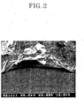
- FIG. 2 shows a Scanning Electron Microscopy (SEM) photograph of portion A of FIG. 1. In FIG. 2, undercuts may be easily seen around the via hole.
- Undercuts such as these may cause a disconnection of metal wiring of the MEMS element or an increase in resistance and a decrease in yield of the device.
- a method for overcoming the undercut problem uses a technique for boring via holes partially into a glass wafer using an etching solution, so that the via holes are not bored completely through the glass wafer.
- the technique does not generate an undercut, some portions of the glass wafer have holes bored therein while other portions do not, and a manufacturing process becomes very complicated. Further, malformed holes may be formed, resulting in decreased yield of devices.
- US 6 284 567 discloses a microsensor and packaging method, in which a contact hole formed in a package wafer is used for connecting the device wafer and packaging wafer together.
- a metal wiring method for an undercut in a MEMS packaging process comprising:
- the invention thus provides a wiring method that allows a metal wiring to be connected to a glass wafer having an undercut formed therein.
- the deposited thin metal film may be resputtered by injecting accelerated gas particles to strike the deposited thin metal film. Further, if the glass wafer has an undercut formed around the hole formed therein, the undercut is filled with the resputtered thin metal film. Further still, if the glass wafer has an undercut formed around the hole formed therein, the ion-milling may be performed until the undercut is removed.
- the accelerated gas particles are preferably argon gas particles.
- FIG. 3 illustrates a view of a MEMS element welded to a silicon substrate or wafer and a glass wafer in an early stage of a packaging process of the MEMS element.
- a MEMS element 23 is welded to a silicon substrate 22, and a glass wafer 24 is welded to an upper portion of the silicon substrate 22, on which the MEMS element 23 is welded.
- a silicon wafer may be used in place of the glass wafer 24.
- the silicon substrate 22 may be formed of single-crystalline silicon, polycrystalline silicon or amorphous silicon and an SOI wafer.
- the MEMS element 23 and silicon substrate 22 are connected using a wiring (not shown).
- a via hole 26 is bored through the glass wafer 24 prior to the glass wafer 24 being welded to the silicon substrate 22.
- an undercut 28 is formed on a portion of the glass wafer 24 adjacent to a bottom of the via hole 26. Then the glass wafer 24 is welded to the silicon substrate 22 having the MEMS element 23 welded thereon. As described above, the undercut 28 may cause a disconnection in a wiring to be added later, or an increase in resistance and decrease in device yield.
- a via hole may be bored into a boundary of a silicon substrate and a glass wafer after the glass wafer and the silicon substrate have been welded together.
- a specific wiring method of depositing and shaping metal on a structure may be adapted for use in the present invention.
- aluminum is used for deposition of the wiring.
- FIG. 4 illustrates a cross sectional view of the MEMS package of FIG. 3 having aluminum 27 deposited thereon. As shown in FIG. 4, the aluminum 27 is not deposited in the undercuts 28 of the via hole 26 in the glass wafer 24. Therefore, a disconnection of metal wiring occurs at the undercuts 28 where the aluminum 27 is not deposited.
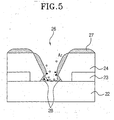
- the present invention provides for ion-milling of the deposited aluminum, as illustrated in FIG. 5.
- FIG. 5 illustrates a view of the MEMS package of FIG. 4, showing a milling process of the deposited aluminum by an ion-milling device (not shown).
- a milling processing time varies according to a kind of ion-milling device and power used. However, it is preferable for the milling processing time to be from about 30 minutes to about one hour.
- the argon (Ar) particles fall almost vertically, so that the aluminum particles at the bottom of the via hole 26 are etched gradually toward the undercuts 28. As a result, the mealed aluminum fills up the undercut portions, and thus the undercuts 28 are removed.
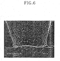
- FIG. 6 is an SEM photograph of a MEMS package having aluminum deposited thereon, and the deposited aluminum being mealed. It may be seen from FIG. 6 that milling the aluminum results in undercut portions being resputtered by the aluminum, so that the aluminum is deposited in the undercuts. Therefore, disconnection of the metal wiring at the undercut portions is prevented.
- a wiring method capable of removing undercuts according to an embodiment of the present invention will be described hereinafter with reference to the flow chart of FIG. 7.
- a MEMS element is welded to a silicon wafer (S702).
- a via hole is bored through a glass wafer to be welded to the silicon wafer having the MEMS element welded thereto (S704).
- the glass wafer with the via hole bored therethrough is welded to the silicon wafer (S706).
- aluminum is deposited onto the welded glass wafer and the silicon wafer using an aluminum sputter process (S708).
- the aluminum deposited to the MEMS package is mealed using an ion-milling device (S710).
- the process described above may be used for all manufacturing processes for wafer level packaging using glass wafers.
- the present invention it is possible to connect metal wiring to via holes having undercuts by using an ion-milling device, so that electrical disconnection of the metal wiring due to the undercuts is prevented. Also, since via holes are etched through a glass wafer in the present invention, the manufacturing process for boring the via holes of the present invention is very simple compared with a method using an etching solution to bore via holes. Further, yield can be greatly increased by the method of the present invention compared with existing metal wiring processes.
Landscapes
- Engineering & Computer Science (AREA)
- Computer Hardware Design (AREA)
- Microelectronics & Electronic Packaging (AREA)
- Micromachines (AREA)
- Internal Circuitry In Semiconductor Integrated Circuit Devices (AREA)
- Coating With Molten Metal (AREA)
Abstract
Description
- The present invention relates to MEMS (Micro-Electronic Mechanical System) technology. More particularly, the present invention relates to a metal wiring method capable of connecting a metal wiring to a via hole having an undercut.
- Rapid growth in the MEMS market is expected, as MEMS technology adopts semiconductor manufacturing techniques, thereby realizing bioengineering related technology and products such as protein chips, DNA chips and micro machining, which are nano-meter level microminiature three-dimensional precision machinery structures.
- MEMS technology adopts semiconductor fine manufacturing techniques, which repeat steps such as vapor deposition and etching, thereby enabling mass production of microminiature products at low prices. MEMS technology also uses electrostatic force, which is an attraction between charges, and surface tension as a driving force to generate current, thereby greatly lowering power consumption. The importance of MEMS technology grows as nano-technology and System On Chip (SOC) technology are developed.
- Since a MEMS element may be easily broken, MEMS elements are tightly packaged or, more preferably, hermetically sealed, in order to be protected from dangerous circumstances.
- A MEMS element packaged in this way may be referred to as a MEMS.
- FIG. 1 illustrates a cross sectional view of a
MEMS element 13 welded to a silicon wafer orsubstrate 12 and aglass wafer 14 according to the prior art. - Referring to FIG. 1, the
MEMS element 13 is layered on thesilicon substrate 12, and theglass wafer 14 is welded onto thesilicon substrate 12 having theMEMS element 13 layered thereon. - A gyro chip, for example, may be used for the
MEMS element 13, and an SOI (Silicon On Insulator) wafer may be used for thesilicon substrate 12. - The
silicon substrate 12 and theglass wafer 14 are welded using an anodic bonding technique, enabling hermetically sealed packaging when adapted to theMEMS element 13. - To connect wiring to the SOI wafer or
silicon substrate 12, aglass wafer 14 having a via hole therein is used. A problem arises, however, when a via hole is bored into theglass wafer 14. Namely, anundercut 15 is formed on theglass wafer 14 when the via hole is bored therethrough. Evidence that such an undercut is formed may be seen in FIG. 2, which shows a Scanning Electron Microscopy (SEM) photograph of portion A of FIG. 1. In FIG. 2, undercuts may be easily seen around the via hole. - Undercuts such as these may cause a disconnection of metal wiring of the MEMS element or an increase in resistance and a decrease in yield of the device.
- A method has been suggested for overcoming the undercut problem that uses a technique for boring via holes partially into a glass wafer using an etching solution, so that the via holes are not bored completely through the glass wafer. However, although the technique does not generate an undercut, some portions of the glass wafer have holes bored therein while other portions do not, and a manufacturing process becomes very complicated. Further, malformed holes may be formed, resulting in decreased yield of devices.
- A manufacturing process becomes very simple if via holes are bored completely through the glass wafers. However, in such a case, excessive vapor deposition of a thin metal film for wiring is necessary, and the wiring may still be disconnected, or a yield of devices may be decreased.
-
US 6 284 567 discloses a microsensor and packaging method, in which a contact hole formed in a package wafer is used for connecting the device wafer and packaging wafer together. - According to the invention, there is provided a metal wiring method for an undercut in a MEMS packaging process, the method comprising:
- disposing a MEMS element on a silicon substrate;
- welding a glass wafer to an upper portion of the silicon substrate having the MEMS element disposed thereon, the glass wafer having a hole formed therein for connecting a metal wiring from above the glass wafer to the upper portion of the substrate and having an undercut at the bottom of the hole;
- depositing a thin metal film for the metal wiring in the hole,
- The invention thus provides a wiring method that allows a metal wiring to be connected to a glass wafer having an undercut formed therein.
- In the ion-milling of the method described above, the deposited thin metal film may be resputtered by injecting accelerated gas particles to strike the deposited thin metal film. Further, if the glass wafer has an undercut formed around the hole formed therein, the undercut is filled with the resputtered thin metal film. Further still, if the glass wafer has an undercut formed around the hole formed therein, the ion-milling may be performed until the undercut is removed. The accelerated gas particles are preferably argon gas particles.
- The above and other features and advantages of the present invention will become more apparent to those of ordinary skill in the art by describing in detail preferred embodiments thereof with reference to the attached drawings in which:
- FIG. 1 illustrates a cross sectional view of a MEMS element welded to a silicon wafer and a glass wafer;
- FIG. 2 is a SEM photograph of a portion A of FIG. 1;
- FIG. 3 illustrates a cross sectional view of a MEMS element welded to a silicon wafer and a glass wafer in accordance with the present invention;
- FIG. 4 illustrates a cross sectional view of a MEMS package of FIG. 3 on which aluminum is deposited;
- FIG. 5 illustrates a view of the MEMS package of FIG. 4, showing a milling process of the deposited aluminum by using an ion-milling device;
- FIG. 6 is an SEM photograph of a MEMS package having aluminum deposited thereon, and the deposited aluminum being mealed, in accordance with the present invention; and
- FIG. 7 is a flow chart illustrating a wiring method capable of removing undercuts according to an embodiment of the present invention.
- The present invention will be described more fully hereinafter with reference to the accompanying drawings, in which preferred embodiments of the invention are shown. The invention may, however, be embodied in different forms and should not be construed as limited to the embodiments set forth herein. Rather, these embodiments are provided so that this disclosure will be thorough and complete, and will fully convey the scope of the invention to those skilled in the art. In the drawings, the thickness of layers and regions are exaggerated for clarity. It will also be understood that when a layer is referred to as being "on" another layer or substrate, it can be directly on the other layer or substrate, or intervening layers may also be present. Further, it will be understood that when a layer is referred to as being "under" another layer, it can be directly under, and one or more intervening layers may also be present. In addition, it will also be understood that when a layer is referred to as being "between" two layers, it can be the only layer between the two layers, or one or more intervening layers may also be present. Like numbers refer to like elements throughout.
- FIG. 3 illustrates a view of a MEMS element welded to a silicon substrate or wafer and a glass wafer in an early stage of a packaging process of the MEMS element.
- Referring to FIG. 3, a
MEMS element 23 is welded to asilicon substrate 22, and aglass wafer 24 is welded to an upper portion of thesilicon substrate 22, on which theMEMS element 23 is welded. In an alternate embodiment of the present invention, a silicon wafer may be used in place of theglass wafer 24. Thesilicon substrate 22 may be formed of single-crystalline silicon, polycrystalline silicon or amorphous silicon and an SOI wafer. - The
MEMS element 23 andsilicon substrate 22 are connected using a wiring (not shown). - For the wiring, a
via hole 26 is bored through theglass wafer 24 prior to theglass wafer 24 being welded to thesilicon substrate 22. Here, an undercut 28 is formed on a portion of theglass wafer 24 adjacent to a bottom of thevia hole 26. Then theglass wafer 24 is welded to thesilicon substrate 22 having theMEMS element 23 welded thereon. As described above, theundercut 28 may cause a disconnection in a wiring to be added later, or an increase in resistance and decrease in device yield. - In accordance with another embodiment of the present invention, instead of boring the
via hole 26 through theglass wafer 24 prior to welding theglass wafer 24 to thesilicon substrate 22, a via hole may be bored into a boundary of a silicon substrate and a glass wafer after the glass wafer and the silicon substrate have been welded together. - To electrically connect the
MEMS element 23 with thesilicon substrate 22, various wiring methods may be used. A specific wiring method of depositing and shaping metal on a structure may be adapted for use in the present invention. In an embodiment of the present invention, aluminum is used for deposition of the wiring. - FIG. 4 illustrates a cross sectional view of the MEMS package of FIG. 3 having
aluminum 27 deposited thereon. As shown in FIG. 4, thealuminum 27 is not deposited in theundercuts 28 of the viahole 26 in theglass wafer 24. Therefore, a disconnection of metal wiring occurs at theundercuts 28 where thealuminum 27 is not deposited. - To resolve this problem, the present invention provides for ion-milling of the deposited aluminum, as illustrated in FIG. 5.
- FIG. 5 illustrates a view of the MEMS package of FIG. 4, showing a milling process of the deposited aluminum by an ion-milling device (not shown).
- As shown in FIG. 5, when the ion-milling device (not shown) is used for milling the
aluminum 27, argon (Ar) particles having strong energy due to a thermoelectric effect resputter and reflow aluminum particles at a bottom of the viahole 26 adjacent to theundercuts 28. - After
aluminum 27 is deposited to a thickness of about 5µm, a milling processing time varies according to a kind of ion-milling device and power used. However, it is preferable for the milling processing time to be from about 30 minutes to about one hour. - In the milling process, the argon (Ar) particles fall almost vertically, so that the aluminum particles at the bottom of the via
hole 26 are etched gradually toward theundercuts 28. As a result, the mealed aluminum fills up the undercut portions, and thus theundercuts 28 are removed. - FIG. 6 is an SEM photograph of a MEMS package having aluminum deposited thereon, and the deposited aluminum being mealed. It may be seen from FIG. 6 that milling the aluminum results in undercut portions being resputtered by the aluminum, so that the aluminum is deposited in the undercuts. Therefore, disconnection of the metal wiring at the undercut portions is prevented.
- A wiring method capable of removing undercuts according to an embodiment of the present invention will be described hereinafter with reference to the flow chart of FIG. 7.
- First, a MEMS element is welded to a silicon wafer (S702). Next, a via hole is bored through a glass wafer to be welded to the silicon wafer having the MEMS element welded thereto (S704). Then, the glass wafer with the via hole bored therethrough is welded to the silicon wafer (S706).
- For metal wiring, aluminum is deposited onto the welded glass wafer and the silicon wafer using an aluminum sputter process (S708). The aluminum deposited to the MEMS package is mealed using an ion-milling device (S710).
- The process described above may be used for all manufacturing processes for wafer level packaging using glass wafers.
- With the present invention, it is possible to connect metal wiring to via holes having undercuts by using an ion-milling device, so that electrical disconnection of the metal wiring due to the undercuts is prevented. Also, since via holes are etched through a glass wafer in the present invention, the manufacturing process for boring the via holes of the present invention is very simple compared with a method using an etching solution to bore via holes. Further, yield can be greatly increased by the method of the present invention compared with existing metal wiring processes.
- Preferred embodiments of the present invention have been disclosed herein. It will be understood by those of ordinary skill in the art that various changes in form and details may be made without departing from the scope of the present invention as set forth in the following claims.
Claims (5)
- A metal wiring method for an undercut in a MEMS packaging process, the method comprising:disposing a MEMS element (23) on a silicon substrate (22);welding a glass wafer (24) to an upper portion of the silicon substrate (22) having the MEMS element (23) disposed thereon, the glass wafer (24) having a hole (26) formed therein for connecting a metal wiring from above the glass wafer (24) to the upper portion of the substrate (22) and having an undercut (28) at the bottom of the hole;depositing a thin metal film (27) for the metal wiring in the hole,characterised in that the method further comprises ion-milling the deposited thin metal film at the bottom of the hole.
- The method as claimed in claim 1, wherein in the ion-milling, the deposited thin metal film (27) is resputtered by injecting accelerated gas particles to strike the deposited thin metal film.
- The method as claimed in claim 2, wherein if the glass wafer has an undercut (28) formed around the hole formed therein, the undercut is filled with the resputtered thin metal film.
- The method as claimed in claim 3, wherein when the glass wafer has the undercut (28) formed around the hole (26) formed therein, the ion-milling is performed until the undercut is removed.
- The method as claimed in any one of claims 2 to 4, wherein the accelerated gas particles are argon gas particles.
Applications Claiming Priority (2)
| Application Number | Priority Date | Filing Date | Title |
|---|---|---|---|
| KR2002063608 | 2002-10-17 | ||
| KR10-2002-0063608A KR100461002B1 (en) | 2002-10-17 | 2002-10-17 | Metal line method even though it has undercut |
Publications (3)
| Publication Number | Publication Date |
|---|---|
| EP1411025A2 EP1411025A2 (en) | 2004-04-21 |
| EP1411025A3 EP1411025A3 (en) | 2004-11-03 |
| EP1411025B1 true EP1411025B1 (en) | 2007-09-19 |
Family
ID=36592652
Family Applications (1)
| Application Number | Title | Priority Date | Filing Date |
|---|---|---|---|
| EP03256418A Expired - Lifetime EP1411025B1 (en) | 2002-10-17 | 2003-10-10 | Metal wiring method for an undercut |
Country Status (9)
| Country | Link |
|---|---|
| US (1) | US6835594B2 (en) |
| EP (1) | EP1411025B1 (en) |
| JP (1) | JP2004136435A (en) |
| KR (1) | KR100461002B1 (en) |
| AT (1) | ATE373623T1 (en) |
| DE (1) | DE60316394T2 (en) |
| DK (1) | DK1411025T3 (en) |
| ES (1) | ES2294247T3 (en) |
| TW (1) | TWI233917B (en) |
Families Citing this family (2)
| Publication number | Priority date | Publication date | Assignee | Title |
|---|---|---|---|---|
| WO2007030484A2 (en) * | 2005-09-06 | 2007-03-15 | Nantero, Inc. | Nanotube fabric-based sensor systems and methods of making same |
| US7915696B2 (en) * | 2007-10-24 | 2011-03-29 | General Electric Company | Electrical connection through a substrate to a microelectromechanical device |
Family Cites Families (13)
| Publication number | Priority date | Publication date | Assignee | Title |
|---|---|---|---|---|
| JPH047836A (en) * | 1990-04-26 | 1992-01-13 | Toshiba Corp | Semiconductor device and manufacture thereof |
| US5198390A (en) * | 1992-01-16 | 1993-03-30 | Cornell Research Foundation, Inc. | RIE process for fabricating submicron, silicon electromechanical structures |
| US5468595A (en) * | 1993-01-29 | 1995-11-21 | Electron Vision Corporation | Method for three-dimensional control of solubility properties of resist layers |
| US5363021A (en) * | 1993-07-12 | 1994-11-08 | Cornell Research Foundation, Inc. | Massively parallel array cathode |
| EP0735577A3 (en) * | 1994-12-14 | 1997-04-02 | Applied Materials Inc | Deposit process and apparatus |
| US5610431A (en) * | 1995-05-12 | 1997-03-11 | The Charles Stark Draper Laboratory, Inc. | Covers for micromechanical sensors and other semiconductor devices |
| KR100442824B1 (en) * | 1997-05-12 | 2004-09-18 | 삼성전자주식회사 | A micromachine and a method for fabricating the same |
| US6333560B1 (en) * | 1999-01-14 | 2001-12-25 | International Business Machines Corporation | Process and structure for an interlock and high performance multilevel structures for chip interconnects and packaging technologies |
| EP1050905B1 (en) * | 1999-05-07 | 2017-06-21 | Shinko Electric Industries Co. Ltd. | Method of producing a semiconductor device with insulating layer |
| KR100314622B1 (en) * | 1999-06-15 | 2001-11-17 | 이형도 | Micro sensor and it's method of package |
| JP3872936B2 (en) * | 2000-06-30 | 2007-01-24 | 株式会社東芝 | Manufacturing method of magnetoresistive effect element and ferromagnetic tunnel junction element |
| JP2002043317A (en) * | 2000-07-27 | 2002-02-08 | Sony Corp | Method for manufacturing semiconductor device |
| US6566274B1 (en) * | 2001-11-28 | 2003-05-20 | Unaxis Balzer Limited | Lithography process for transparent substrates |
-
2002
- 2002-10-17 KR KR10-2002-0063608A patent/KR100461002B1/en not_active Expired - Fee Related
-
2003
- 2003-10-10 ES ES03256418T patent/ES2294247T3/en not_active Expired - Lifetime
- 2003-10-10 DK DK03256418T patent/DK1411025T3/en active
- 2003-10-10 AT AT03256418T patent/ATE373623T1/en not_active IP Right Cessation
- 2003-10-10 DE DE60316394T patent/DE60316394T2/en not_active Expired - Fee Related
- 2003-10-10 EP EP03256418A patent/EP1411025B1/en not_active Expired - Lifetime
- 2003-10-16 JP JP2003356508A patent/JP2004136435A/en active Pending
- 2003-10-17 US US10/686,769 patent/US6835594B2/en not_active Expired - Lifetime
- 2003-10-17 TW TW092128849A patent/TWI233917B/en not_active IP Right Cessation
Also Published As
| Publication number | Publication date |
|---|---|
| EP1411025A2 (en) | 2004-04-21 |
| DK1411025T3 (en) | 2007-11-05 |
| ES2294247T3 (en) | 2008-04-01 |
| TW200426110A (en) | 2004-12-01 |
| DE60316394D1 (en) | 2007-10-31 |
| ATE373623T1 (en) | 2007-10-15 |
| EP1411025A3 (en) | 2004-11-03 |
| KR100461002B1 (en) | 2004-12-09 |
| TWI233917B (en) | 2005-06-11 |
| KR20040034949A (en) | 2004-04-29 |
| US6835594B2 (en) | 2004-12-28 |
| DE60316394T2 (en) | 2008-01-17 |
| US20040203186A1 (en) | 2004-10-14 |
| JP2004136435A (en) | 2004-05-13 |
Similar Documents
| Publication | Publication Date | Title |
|---|---|---|
| CN102381677B (en) | Composite wafer semiconductor element and method for forming same | |
| US9776856B2 (en) | Vacuum sealed MEMS and CMOS package | |
| US6660564B2 (en) | Wafer-level through-wafer packaging process for MEMS and MEMS package produced thereby | |
| CN103420325B (en) | For the method manufacturing the component of hybrid integrated | |
| US7767484B2 (en) | Method for sealing and backside releasing of microelectromechanical systems | |
| US7642611B2 (en) | Sensor device, sensor system and methods for manufacturing them | |
| US6429511B2 (en) | Microcap wafer-level package | |
| US6376280B1 (en) | Microcap wafer-level package | |
| US20030183920A1 (en) | Hermetic electric component package | |
| WO2009111874A1 (en) | Low-temperature wafer level processing for mems devices | |
| JP2005129888A (en) | Sensor device and sensor system, and manufacturing method therefor | |
| US20180202807A1 (en) | Micromechanical sensor | |
| WO2016053584A1 (en) | Method for forming through substrate vias | |
| US9266721B2 (en) | Eutectic bonding of thin chips on a carrier substrate | |
| EP1199744B1 (en) | Microcap wafer-level package | |
| CN118355484A (en) | Via hole including electroplating layer and method for making via hole | |
| EP1411025A2 (en) | Metal wiring method for an undercut | |
| JP2003326500A (en) | Sheet substrate structure for wafer process and method of manufacturing mems element using the sheet substrate | |
| CN1834000A (en) | Round piece class airtight packing technique having low depth-width ratio through hole | |
| CN1496951A (en) | Metal Routing Methods for Undercuts | |
| US12630419B2 (en) | Production method for a micromechanical sensor apparatus, and corresponding micromechanical sensor apparatus | |
| US20230406697A1 (en) | Production method for a micromechanical sensor apparatus, and corresponding micromechanical sensor apparatus | |
| JP2006186357A (en) | Sensor device and manufacturing method thereof | |
| JP2006201158A (en) | Sensor | |
| JP2005271085A (en) | Method for assembling MEMS and IC on substrate and MEMS device |
Legal Events
| Date | Code | Title | Description |
|---|---|---|---|
| PUAI | Public reference made under article 153(3) epc to a published international application that has entered the european phase |
Free format text: ORIGINAL CODE: 0009012 |
|
| AK | Designated contracting states |
Kind code of ref document: A2 Designated state(s): AT BE BG CH CY CZ DE DK EE ES FI FR GB GR HU IE IT LI LU MC NL PT RO SE SI SK TR |
|
| AX | Request for extension of the european patent |
Extension state: AL LT LV MK |
|
| RIN1 | Information on inventor provided before grant (corrected) |
Inventor name: JUNG, KYU-DONG Inventor name: KANG, SEOK-JIN Inventor name: KANG, JUNG-HO Inventor name: JUN, CHAN-BONG Inventor name: HONG, SEOG-WOO Inventor name: KIM, JONG-SEOK Inventor name: SHONG, CI-MOO Inventor name: LEE, MOON-CHUL Inventor name: CHUNG, SEOK-WHAN |
|
| RIN1 | Information on inventor provided before grant (corrected) |
Inventor name: KIM, JONG-SEOK Inventor name: HONG, SEOG-WOO Inventor name: JUNG, KYU-DONG Inventor name: KANG, SEOK-JIN Inventor name: KANG, JUNG-HO Inventor name: JUN, CHAN-BONG Inventor name: CHUNG, SEOK-WHAN Inventor name: LEE, MOON-CHUL Inventor name: SHONG, CI-MOO |
|
| PUAL | Search report despatched |
Free format text: ORIGINAL CODE: 0009013 |
|
| AK | Designated contracting states |
Kind code of ref document: A3 Designated state(s): AT BE BG CH CY CZ DE DK EE ES FI FR GB GR HU IE IT LI LU MC NL PT RO SE SI SK TR |
|
| AX | Request for extension of the european patent |
Extension state: AL LT LV MK |
|
| RIC1 | Information provided on ipc code assigned before grant |
Ipc: 7B 81C 1/00 A Ipc: 7B 81B 1/00 B Ipc: 7B 81B 7/00 B |
|
| 17P | Request for examination filed |
Effective date: 20050223 |
|
| AKX | Designation fees paid |
Designated state(s): AT BE BG CH CY CZ DE DK EE ES FI FR GB GR HU IE IT LI LU MC NL PT RO SE SI SK TR |
|
| 17Q | First examination report despatched |
Effective date: 20060419 |
|
| GRAP | Despatch of communication of intention to grant a patent |
Free format text: ORIGINAL CODE: EPIDOSNIGR1 |
|
| GRAS | Grant fee paid |
Free format text: ORIGINAL CODE: EPIDOSNIGR3 |
|
| GRAA | (expected) grant |
Free format text: ORIGINAL CODE: 0009210 |
|
| AK | Designated contracting states |
Kind code of ref document: B1 Designated state(s): AT BE BG CH CY CZ DE DK EE ES FI FR GB GR HU IE IT LI LU MC NL PT RO SE SI SK TR |
|
| REG | Reference to a national code |
Ref country code: GB Ref legal event code: FG4D |
|
| REG | Reference to a national code |
Ref country code: CH Ref legal event code: EP |
|
| REF | Corresponds to: |
Ref document number: 60316394 Country of ref document: DE Date of ref document: 20071031 Kind code of ref document: P |
|
| REG | Reference to a national code |
Ref country code: DK Ref legal event code: T3 |
|
| REG | Reference to a national code |
Ref country code: IE Ref legal event code: FG4D |
|
| PG25 | Lapsed in a contracting state [announced via postgrant information from national office to epo] |
Ref country code: CH Free format text: LAPSE BECAUSE OF FAILURE TO SUBMIT A TRANSLATION OF THE DESCRIPTION OR TO PAY THE FEE WITHIN THE PRESCRIBED TIME-LIMIT Effective date: 20070919 Ref country code: LI Free format text: LAPSE BECAUSE OF FAILURE TO SUBMIT A TRANSLATION OF THE DESCRIPTION OR TO PAY THE FEE WITHIN THE PRESCRIBED TIME-LIMIT Effective date: 20070919 Ref country code: AT Free format text: LAPSE BECAUSE OF FAILURE TO SUBMIT A TRANSLATION OF THE DESCRIPTION OR TO PAY THE FEE WITHIN THE PRESCRIBED TIME-LIMIT Effective date: 20070919 |
|
| ET | Fr: translation filed | ||
| REG | Reference to a national code |
Ref country code: CH Ref legal event code: PL |
|
| REG | Reference to a national code |
Ref country code: ES Ref legal event code: FG2A Ref document number: 2294247 Country of ref document: ES Kind code of ref document: T3 |
|
| PG25 | Lapsed in a contracting state [announced via postgrant information from national office to epo] |
Ref country code: GR Free format text: LAPSE BECAUSE OF FAILURE TO SUBMIT A TRANSLATION OF THE DESCRIPTION OR TO PAY THE FEE WITHIN THE PRESCRIBED TIME-LIMIT Effective date: 20071220 |
|
| PG25 | Lapsed in a contracting state [announced via postgrant information from national office to epo] |
Ref country code: CZ Free format text: LAPSE BECAUSE OF FAILURE TO SUBMIT A TRANSLATION OF THE DESCRIPTION OR TO PAY THE FEE WITHIN THE PRESCRIBED TIME-LIMIT Effective date: 20070919 Ref country code: MC Free format text: LAPSE BECAUSE OF NON-PAYMENT OF DUE FEES Effective date: 20071031 Ref country code: SK Free format text: LAPSE BECAUSE OF FAILURE TO SUBMIT A TRANSLATION OF THE DESCRIPTION OR TO PAY THE FEE WITHIN THE PRESCRIBED TIME-LIMIT Effective date: 20070919 Ref country code: PT Free format text: LAPSE BECAUSE OF FAILURE TO SUBMIT A TRANSLATION OF THE DESCRIPTION OR TO PAY THE FEE WITHIN THE PRESCRIBED TIME-LIMIT Effective date: 20080219 |
|
| PG25 | Lapsed in a contracting state [announced via postgrant information from national office to epo] |
Ref country code: RO Free format text: LAPSE BECAUSE OF FAILURE TO SUBMIT A TRANSLATION OF THE DESCRIPTION OR TO PAY THE FEE WITHIN THE PRESCRIBED TIME-LIMIT Effective date: 20070919 Ref country code: SE Free format text: LAPSE BECAUSE OF FAILURE TO SUBMIT A TRANSLATION OF THE DESCRIPTION OR TO PAY THE FEE WITHIN THE PRESCRIBED TIME-LIMIT Effective date: 20071219 |
|
| PLBE | No opposition filed within time limit |
Free format text: ORIGINAL CODE: 0009261 |
|
| STAA | Information on the status of an ep patent application or granted ep patent |
Free format text: STATUS: NO OPPOSITION FILED WITHIN TIME LIMIT |
|
| 26N | No opposition filed |
Effective date: 20080620 |
|
| PG25 | Lapsed in a contracting state [announced via postgrant information from national office to epo] |
Ref country code: IE Free format text: LAPSE BECAUSE OF NON-PAYMENT OF DUE FEES Effective date: 20071010 |
|
| PGFP | Annual fee paid to national office [announced via postgrant information from national office to epo] |
Ref country code: NL Payment date: 20081005 Year of fee payment: 6 |
|
| PG25 | Lapsed in a contracting state [announced via postgrant information from national office to epo] |
Ref country code: EE Free format text: LAPSE BECAUSE OF FAILURE TO SUBMIT A TRANSLATION OF THE DESCRIPTION OR TO PAY THE FEE WITHIN THE PRESCRIBED TIME-LIMIT Effective date: 20070919 |
|
| PGFP | Annual fee paid to national office [announced via postgrant information from national office to epo] |
Ref country code: DE Payment date: 20081014 Year of fee payment: 6 Ref country code: DK Payment date: 20081013 Year of fee payment: 6 |
|
| PGFP | Annual fee paid to national office [announced via postgrant information from national office to epo] |
Ref country code: ES Payment date: 20081121 Year of fee payment: 6 Ref country code: FI Payment date: 20081014 Year of fee payment: 6 |
|
| PGFP | Annual fee paid to national office [announced via postgrant information from national office to epo] |
Ref country code: BE Payment date: 20081010 Year of fee payment: 6 |
|
| PGFP | Annual fee paid to national office [announced via postgrant information from national office to epo] |
Ref country code: FR Payment date: 20081014 Year of fee payment: 6 |
|
| PG25 | Lapsed in a contracting state [announced via postgrant information from national office to epo] |
Ref country code: SI Free format text: LAPSE BECAUSE OF FAILURE TO SUBMIT A TRANSLATION OF THE DESCRIPTION OR TO PAY THE FEE WITHIN THE PRESCRIBED TIME-LIMIT Effective date: 20070919 |
|
| PGFP | Annual fee paid to national office [announced via postgrant information from national office to epo] |
Ref country code: GB Payment date: 20081008 Year of fee payment: 6 |
|
| PG25 | Lapsed in a contracting state [announced via postgrant information from national office to epo] |
Ref country code: CY Free format text: LAPSE BECAUSE OF FAILURE TO SUBMIT A TRANSLATION OF THE DESCRIPTION OR TO PAY THE FEE WITHIN THE PRESCRIBED TIME-LIMIT Effective date: 20070919 |
|
| PG25 | Lapsed in a contracting state [announced via postgrant information from national office to epo] |
Ref country code: BG Free format text: LAPSE BECAUSE OF FAILURE TO SUBMIT A TRANSLATION OF THE DESCRIPTION OR TO PAY THE FEE WITHIN THE PRESCRIBED TIME-LIMIT Effective date: 20071219 Ref country code: LU Free format text: LAPSE BECAUSE OF NON-PAYMENT OF DUE FEES Effective date: 20071010 |
|
| PG25 | Lapsed in a contracting state [announced via postgrant information from national office to epo] |
Ref country code: HU Free format text: LAPSE BECAUSE OF FAILURE TO SUBMIT A TRANSLATION OF THE DESCRIPTION OR TO PAY THE FEE WITHIN THE PRESCRIBED TIME-LIMIT Effective date: 20080320 Ref country code: TR Free format text: LAPSE BECAUSE OF FAILURE TO SUBMIT A TRANSLATION OF THE DESCRIPTION OR TO PAY THE FEE WITHIN THE PRESCRIBED TIME-LIMIT Effective date: 20070919 |
|
| BERE | Be: lapsed |
Owner name: SAMSUNG ELECTRONICS CO., LTD. Effective date: 20091031 |
|
| REG | Reference to a national code |
Ref country code: NL Ref legal event code: V1 Effective date: 20100501 |
|
| REG | Reference to a national code |
Ref country code: DK Ref legal event code: EBP |
|
| REG | Reference to a national code |
Ref country code: FR Ref legal event code: ST Effective date: 20100630 |
|
| PG25 | Lapsed in a contracting state [announced via postgrant information from national office to epo] |
Ref country code: DE Free format text: LAPSE BECAUSE OF NON-PAYMENT OF DUE FEES Effective date: 20100501 Ref country code: NL Free format text: LAPSE BECAUSE OF NON-PAYMENT OF DUE FEES Effective date: 20100501 Ref country code: FR Free format text: LAPSE BECAUSE OF NON-PAYMENT OF DUE FEES Effective date: 20091102 |
|
| PG25 | Lapsed in a contracting state [announced via postgrant information from national office to epo] |
Ref country code: FI Free format text: LAPSE BECAUSE OF NON-PAYMENT OF DUE FEES Effective date: 20091010 |
|
| PG25 | Lapsed in a contracting state [announced via postgrant information from national office to epo] |
Ref country code: BE Free format text: LAPSE BECAUSE OF NON-PAYMENT OF DUE FEES Effective date: 20091031 |
|
| PG25 | Lapsed in a contracting state [announced via postgrant information from national office to epo] |
Ref country code: GB Free format text: LAPSE BECAUSE OF NON-PAYMENT OF DUE FEES Effective date: 20091010 |
|
| PG25 | Lapsed in a contracting state [announced via postgrant information from national office to epo] |
Ref country code: DK Free format text: LAPSE BECAUSE OF NON-PAYMENT OF DUE FEES Effective date: 20091031 |
|
| PG25 | Lapsed in a contracting state [announced via postgrant information from national office to epo] |
Ref country code: IT Free format text: LAPSE BECAUSE OF NON-PAYMENT OF DUE FEES Effective date: 20071031 |
|
| REG | Reference to a national code |
Ref country code: ES Ref legal event code: FD2A Effective date: 20110303 |
|
| PG25 | Lapsed in a contracting state [announced via postgrant information from national office to epo] |
Ref country code: ES Free format text: LAPSE BECAUSE OF NON-PAYMENT OF DUE FEES Effective date: 20110302 |
|
| PG25 | Lapsed in a contracting state [announced via postgrant information from national office to epo] |
Ref country code: ES Free format text: LAPSE BECAUSE OF NON-PAYMENT OF DUE FEES Effective date: 20091011 |