EP1408576A1 - Band-pass filter - Google Patents
Band-pass filter Download PDFInfo
- Publication number
- EP1408576A1 EP1408576A1 EP20030255936 EP03255936A EP1408576A1 EP 1408576 A1 EP1408576 A1 EP 1408576A1 EP 20030255936 EP20030255936 EP 20030255936 EP 03255936 A EP03255936 A EP 03255936A EP 1408576 A1 EP1408576 A1 EP 1408576A1
- Authority
- EP
- European Patent Office
- Prior art keywords
- substrate
- band
- microstrip
- conductor
- pass filter
- Prior art date
- Legal status (The legal status is an assumption and is not a legal conclusion. Google has not performed a legal analysis and makes no representation as to the accuracy of the status listed.)
- Withdrawn
Links
- 239000004020 conductor Substances 0.000 claims abstract description 85
- 239000000758 substrate Substances 0.000 claims abstract description 65
- 230000008878 coupling Effects 0.000 claims description 7
- 238000010168 coupling process Methods 0.000 claims description 7
- 238000005859 coupling reaction Methods 0.000 claims description 7
- 239000000853 adhesive Substances 0.000 description 1
- 230000001070 adhesive effect Effects 0.000 description 1
- 238000000034 method Methods 0.000 description 1
- 238000005476 soldering Methods 0.000 description 1
Images


Classifications
-
- H—ELECTRICITY
- H01—ELECTRIC ELEMENTS
- H01P—WAVEGUIDES; RESONATORS, LINES, OR OTHER DEVICES OF THE WAVEGUIDE TYPE
- H01P1/00—Auxiliary devices
- H01P1/20—Frequency-selective devices, e.g. filters
- H01P1/201—Filters for transverse electromagnetic waves
- H01P1/203—Strip line filters
Definitions
- the present invention relates to a band-pass filter having microstrip conductors, and particularly to a band-pass filter having triangular microstrip conductors.
- band-pass filters having triangular microstrip conductors (sometimes called cymbal band-pass filters) are being studied.
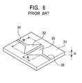
- Fig. 6 shows a conventional cymbal band-pass filter, which includes a substrate 31 having two triangular microstrip conductors 32 and 33 formed on the upper surface thereof.
- the first microstrip conductor 32 and the second microstrip conductor 33 are shaped like isosceles triangles of the same size, and are disposed so that corresponding sides (bases) of the two microstrip conductors 32 and 33 are parallel to each other.
- the distance between the parallel bases and the sizes of the microstrip conductors determine characteristics such as the band-pass center frequency, bandwidth, loss, and skirt characteristics.
- the length W of each base is about 4.77 mm
- the distance G (not shown in Fig. 6) between the bases is 0.15 mm
- the height K from each base to the opposite apex is 0.6 mm.
- the thickness H of the substrate 31 is 0.25 mm.
- the substrate 31 has a first conductive line 34 and a second conductive line 35.
- the first conductive line 34 is connected to the apex opposite to the base of the first microstrip conductor 32.
- the second conductive line 35 is connected to the apex opposite to the base of the second microstrip conductor 33.
- the substrate 31 further includes a grounding conductor (not shown in Fig. 6) formed on its rear surface.
- the conductive lines 34 and 35 have a characteristic impedance of, for example, 50 ohm.
- One of the conductive lines 34 and 35 is used for signal input and the other for signal output. Useful information about these band-pass filters can be found in non-patent document, IEEE TRANSACTIONS ON MICROWAVE THEORY AND TECHNIQUES, VOL. 50. NO. 5, MAY 2002, P. 1431-1432, for example.
- the apexes opposite to the bases of the two triangular microstrip conductors function as the input and output terminals of the band-pass filter, where the distance between the input and output terminals is about 1.35 mm. This size of about 1.35 mm is not satisfactory to meet recent demands for more compact high-frequency devices. Unfortunately, reducing the size of microstrip conductors causes another problem with the performance of the band-pass filter.
- an object of the present invention is to provide a compact band-pass filter while still maintaining high electrical performance.
- a band-pass filter includes a first substrate having a first triangular microstrip conductor formed on a first surface thereof and a first grounding conductor formed on a second surface thereof; a second substrate having a second triangular microstrip conductor formed on a first surface thereof and a second grounding conductor formed on a second surface thereof; and a third substrate having a first conductive line and a second conductive line formed on a first surface thereof and a third grounding conductor formed on a second surface thereof.
- the first substrate and the second substrate are joined at the second surfaces, and are disposed on the first surface of the third substrate such that a first side of each of the first and second microstrip conductors is parallel to the first surface of the third substrate. Furthermore, the apex opposite to the first side of the first microstrip conductor is connected to the first conductive line, the apex opposite to the first side of the second microstrip conductor is connected to the second conductive line, and the first and second grounding conductors are connected to the third grounding conductor.
- the distance between the apexes of the microstrip conductors, i.e., the input and output terminals of the band-pass filter can be reduced dramatically, thus contributing to compact design of the band-pass filter.
- the band-pass filter may include a fourth substrate disposed on the top side of each of the first and second substrates, that is, the top side along the first side of each of the first and second microstrip conductors; and a coupling conductor disposed on the fourth substrate to couple the first and second microstrip conductors with each other.
- the two microstrip conductors are made electrically closer to each other via the coupling conductor, and therefore, are coupled with each other more strongly.
- Fig. 1 is a perspective view of a band-pass filter according to a first embodiment.
- Fig. 2 is a front view of the band-pass filter.
- Fig. 3 is a side view of the band-pass filter.
- Fig. 4 is a perspective view of a band-pass filter according to a second embodiment.
- Fig. 5 is a side view of the band-pass filter shown in Fig. 4.
- the band-pass filter according to the first embodiment of the present invention includes two rectangular substrates of the same size, a first substrate 1 and a second substrate 2, each having a thickness H of 0.25 mm.
- the band-pass filter further includes a third substrate 7.
- the first substrate 1 includes a first triangular microstrip conductor 3 formed on one surface thereof and a grounding conductor 4 formed on the other entire surface thereof.
- the second substrate 2 includes a second triangular microstrip conductor 5 formed on one surface thereof and a grounding conductor 6 formed on the other entire surface thereof.
- the first microstrip conductor 3 and the second microstrip conductor 5 are of the same size.
- the third substrate 7 includes a first conductive line 8 and a second conductive line 9 on its upper surface and a grounding conductor 10 on its entire lower surface.
- the first substrate 1 and the second substrate 2 are jointed at the surfaces having the respective grounding conductors 4 and 6 so that the two grounding conductors 4 and 6 are in contact with each other.
- the main surfaces of each of the first substrate 1 and the second substrate 2 have a side with a length substantially equal to the length W of one side (base) of the corresponding microstrip conductor, and another perpendicular side with a length substantially equal to the height K from the base to the opposite apex of the corresponding microstrip conductor.
- the length W and the height K are about 4.77 mm and about 0.6 mm, respectively, to achieve a band-pass center frequency of 25 GHz.
- the two substrates 1 and 2 thus joined are secured to the upper surface of the third substrate 7 by bonding means such as an adhesive (not shown in Figs. 1 to 3) so that the bases of the microstrip conductors 3 and 5 are distant from and parallel to the upper surface of the third substrate 7 and the apexes of the microstrip conductors 3 and 5 face down.
- This arrangement brings the apexes of the microstrip conductors 3 and 5 into contact with the upper surface of the third substrate 7.
- the two apexes function as the input and output terminals of the band-pass filter.
- Each of the first substrate 1 and the second substrate 2 further includes two notches, one at each corner on the left and right edges of the surface in contact with the upper surface of the third substrate 7.
- the notches on the first substrate 1 and the second substrate 2 are denoted by 1a and 2a, respectively.
- the conductive lines 8 and 9 formed on the upper surface of the substrate 7 have a characteristic impedance of, for example, 50 ohm.
- One of the conductive lines 8 and 9 is used for signal input and the other for signal output.
- the apex opposite to the base of the first microstrip conductor 3 is connected to the first conductive line 8 and the apex opposite to the base of the second microstrip conductor 5 is connected to the second conductive line 9 by bonding means such as soldering.
- the third substrate 7 further includes two through-holes. 11, adjacent to the notches 1a and 2a.
- Each of the through-holes 11 has, on its inner wall, an inner conductor 11a connected to the grounding conductor 10.
- the grounding conductors 4 and 6 exposed at the notches 1a and 2a are connected to the inner conductors 11a in the through-holes 11.
- the grounding conductor 4 of the first substrate 1 and the grounding conductor 6 of the second substrate 2 are electrically conductive with the grounding conductor 10 of the third substrate 7.
- the first microstrip conductor 3 and the second microstrip conductor 5 are coupled with each other around their bases to exhibit predetermined characteristics.
- the distance between the apexes opposite to the bases of the two microstrip conductors, i.e., input and output terminals of the band-pass filter, is about 0.51 mm, which is about one-third of that for a conventional band-pass filter.
- the band-pass filter according to the first embodiment is compact.
- the two substrates 1 and 2 are covered with a shielding case, which is not shown in Figs. 1 to 3.
- a fourth substrate 21 may be provided in order to more strongly couple the first microstrip conductor 3 with the second microstrip conductor 5.
- the fourth substrate 21 is disposed on the top sides of the first substrate 1 and the second substrate 2 such that the fourth substrate 21 extends along the bases of the microstrip conductors 3 and 5.
- the fourth substrate 21 has a coupling conductor 22 on its upper surface.
- the two microstrip conductors 3 and 5 are made electrically closer to each other via the coupling conductor 22, and are therefore coupled with each other more strongly.
- the thickness of the fourth substrate 21 and the width of the coupling conductor 22 affect the strength of coupling between the two microstrip conductors 3 and 5, and hence need to be determined appropriately.
Landscapes
- Physics & Mathematics (AREA)
- Electromagnetism (AREA)
- Control Of Motors That Do Not Use Commutators (AREA)
Abstract
Description
- The present invention relates to a band-pass filter having microstrip conductors, and particularly to a band-pass filter having triangular microstrip conductors.
- Nowadays, band-pass filters having triangular microstrip conductors (sometimes called cymbal band-pass filters) are being studied.
- Fig. 6 shows a conventional cymbal band-pass filter, which includes a
substrate 31 having twotriangular microstrip conductors first microstrip conductor 32 and thesecond microstrip conductor 33 are shaped like isosceles triangles of the same size, and are disposed so that corresponding sides (bases) of the twomicrostrip conductors substrate 31 is 0.25 mm. - Referring again to Fig. 6, the
substrate 31 has a firstconductive line 34 and a secondconductive line 35. The firstconductive line 34 is connected to the apex opposite to the base of thefirst microstrip conductor 32. The secondconductive line 35 is connected to the apex opposite to the base of thesecond microstrip conductor 33. Thesubstrate 31 further includes a grounding conductor (not shown in Fig. 6) formed on its rear surface. Theconductive lines conductive lines - In the band-pass filter described above, the apexes opposite to the bases of the two triangular microstrip conductors function as the input and output terminals of the band-pass filter, where the distance between the input and output terminals is about 1.35 mm. This size of about 1.35 mm is not satisfactory to meet recent demands for more compact high-frequency devices. Unfortunately, reducing the size of microstrip conductors causes another problem with the performance of the band-pass filter.
- Accordingly, an object of the present invention is to provide a compact band-pass filter while still maintaining high electrical performance.
- In order to achieve the object described above, a band-pass filter according to an aspect of the present invention includes a first substrate having a first triangular microstrip conductor formed on a first surface thereof and a first grounding conductor formed on a second surface thereof; a second substrate having a second triangular microstrip conductor formed on a first surface thereof and a second grounding conductor formed on a second surface thereof; and a third substrate having a first conductive line and a second conductive line formed on a first surface thereof and a third grounding conductor formed on a second surface thereof. The first substrate and the second substrate are joined at the second surfaces, and are disposed on the first surface of the third substrate such that a first side of each of the first and second microstrip conductors is parallel to the first surface of the third substrate. Furthermore, the apex opposite to the first side of the first microstrip conductor is connected to the first conductive line, the apex opposite to the first side of the second microstrip conductor is connected to the second conductive line, and the first and second grounding conductors are connected to the third grounding conductor.
- In the band-pass filter described above, the distance between the apexes of the microstrip conductors, i.e., the input and output terminals of the band-pass filter can be reduced dramatically, thus contributing to compact design of the band-pass filter.
- The band-pass filter may include a fourth substrate disposed on the top side of each of the first and second substrates, that is, the top side along the first side of each of the first and second microstrip conductors; and a coupling conductor disposed on the fourth substrate to couple the first and second microstrip conductors with each other.
- In the band-pass filter described above, the two microstrip conductors are made electrically closer to each other via the coupling conductor, and therefore, are coupled with each other more strongly.
-
- Fig. 1 is a perspective view of a band-pass filter according to a first embodiment of the present invention;
- Fig. 2 is a front view of the band-pass filter according to the first embodiment of the present invention;
- Fig. 3 is a side view of the band-pass filter according to the first embodiment of the present invention;
- Fig. 4 is a perspective view of a band-pass filter according to a second embodiment of the present invention;
- Fig. 5 is a side view of the band-pass filter according to the second embodiment of the present invention; and
- Fig. 6 is a perspective view of a conventional band-pass filter.
-
- Band-pass filters according to embodiments of the present invention are illustrated in Figs. 1 to 5. Fig. 1 is a perspective view of a band-pass filter according to a first embodiment. Fig. 2 is a front view of the band-pass filter. Fig. 3 is a side view of the band-pass filter. Fig. 4 is a perspective view of a band-pass filter according to a second embodiment. Fig. 5 is a side view of the band-pass filter shown in Fig. 4.
- Referring to Figs. 1 to 3, the band-pass filter according to the first embodiment of the present invention includes two rectangular substrates of the same size, a
first substrate 1 and asecond substrate 2, each having a thickness H of 0.25 mm. The band-pass filter further includes athird substrate 7. - The
first substrate 1 includes a firsttriangular microstrip conductor 3 formed on one surface thereof and agrounding conductor 4 formed on the other entire surface thereof. - The
second substrate 2 includes a second triangular microstrip conductor 5 formed on one surface thereof and agrounding conductor 6 formed on the other entire surface thereof. Thefirst microstrip conductor 3 and the second microstrip conductor 5 are of the same size. - The
third substrate 7 includes a firstconductive line 8 and a secondconductive line 9 on its upper surface and agrounding conductor 10 on its entire lower surface. - The
first substrate 1 and thesecond substrate 2 are jointed at the surfaces having therespective grounding conductors grounding conductors first substrate 1 and thesecond substrate 2 have a side with a length substantially equal to the length W of one side (base) of the corresponding microstrip conductor, and another perpendicular side with a length substantially equal to the height K from the base to the opposite apex of the corresponding microstrip conductor. The length W and the height K are about 4.77 mm and about 0.6 mm, respectively, to achieve a band-pass center frequency of 25 GHz. - The two
substrates third substrate 7 by bonding means such as an adhesive (not shown in Figs. 1 to 3) so that the bases of themicrostrip conductors 3 and 5 are distant from and parallel to the upper surface of thethird substrate 7 and the apexes of themicrostrip conductors 3 and 5 face down. This arrangement brings the apexes of themicrostrip conductors 3 and 5 into contact with the upper surface of thethird substrate 7. The two apexes function as the input and output terminals of the band-pass filter. - Each of the
first substrate 1 and thesecond substrate 2 further includes two notches, one at each corner on the left and right edges of the surface in contact with the upper surface of thethird substrate 7. The notches on thefirst substrate 1 and thesecond substrate 2 are denoted by 1a and 2a, respectively. - The
conductive lines substrate 7 have a characteristic impedance of, for example, 50 ohm. One of theconductive lines first microstrip conductor 3 is connected to the firstconductive line 8 and the apex opposite to the base of the second microstrip conductor 5 is connected to the secondconductive line 9 by bonding means such as soldering. - The
third substrate 7 further includes two through-holes. 11, adjacent to thenotches holes 11 has, on its inner wall, aninner conductor 11a connected to thegrounding conductor 10. The groundingconductors notches inner conductors 11a in the through-holes 11. As a result, thegrounding conductor 4 of thefirst substrate 1 and thegrounding conductor 6 of thesecond substrate 2 are electrically conductive with the groundingconductor 10 of thethird substrate 7. - According to the structure described above, the
first microstrip conductor 3 and the second microstrip conductor 5 are coupled with each other around their bases to exhibit predetermined characteristics. - The distance between the apexes opposite to the bases of the two microstrip conductors, i.e., input and output terminals of the band-pass filter, is about 0.51 mm, which is about one-third of that for a conventional band-pass filter. Thus, the band-pass filter according to the first embodiment is compact.
- The two
substrates - A
fourth substrate 21 may be provided in order to more strongly couple thefirst microstrip conductor 3 with the second microstrip conductor 5. Referring to Figs. 4 and 5 showing a band-pass filter according to a second embodiment, thefourth substrate 21 is disposed on the top sides of thefirst substrate 1 and thesecond substrate 2 such that thefourth substrate 21 extends along the bases of themicrostrip conductors 3 and 5. Furthermore, thefourth substrate 21 has acoupling conductor 22 on its upper surface. Thus, the twomicrostrip conductors 3 and 5 are made electrically closer to each other via thecoupling conductor 22, and are therefore coupled with each other more strongly. The thickness of thefourth substrate 21 and the width of thecoupling conductor 22 affect the strength of coupling between the twomicrostrip conductors 3 and 5, and hence need to be determined appropriately.
Claims (2)
- A band-pass filter comprising:wherein the first substrate and the second substrate are joined at the second surfaces, and are disposed on the first surface of the third substrate such that a first side of each of the first and second microstrip conductors is parallel to the first surface of the third substrate; anda first substrate including:a first triangular microstrip conductor formed on a first surface thereof; anda first grounding conductor formed on a second surface thereof;a second substrate including:a second triangular microstrip conductor formed on a first surface thereof; anda second grounding conductor formed on a second surface thereof; anda third substrate including:a first conductive line and a second conductive line formed on a first surface thereof; anda third grounding conductor formed on a second surface thereof,
wherein the apex opposite to the first side of the first microstrip conductor is connected to the first conductive line, the apex opposite to the first side of the second microstrip conductor is connected to the second conductive line, and the first and second grounding conductors are connected to the third grounding conductor. - The band-pass filter according to claim 1, further comprising:a fourth substrate disposed on the top side of each of the first and second substrates, the top side being along the first side of each of the first and second microstrip conductors; anda coupling conductor disposed on the fourth substrate to couple the first and second microstrip conductors with each other.
Applications Claiming Priority (2)
| Application Number | Priority Date | Filing Date | Title |
|---|---|---|---|
| JP2002295382 | 2002-10-08 | ||
| JP2002295382A JP2004134894A (en) | 2002-10-08 | 2002-10-08 | Band path filter |
Publications (1)
| Publication Number | Publication Date |
|---|---|
| EP1408576A1 true EP1408576A1 (en) | 2004-04-14 |
Family
ID=32025519
Family Applications (1)
| Application Number | Title | Priority Date | Filing Date |
|---|---|---|---|
| EP20030255936 Withdrawn EP1408576A1 (en) | 2002-10-08 | 2003-09-23 | Band-pass filter |
Country Status (2)
| Country | Link |
|---|---|
| EP (1) | EP1408576A1 (en) |
| JP (1) | JP2004134894A (en) |
Families Citing this family (2)
| Publication number | Priority date | Publication date | Assignee | Title |
|---|---|---|---|---|
| JP4775395B2 (en) * | 2008-03-26 | 2011-09-21 | Tdk株式会社 | Multilayer electronic components |
| JP6962221B2 (en) * | 2018-02-01 | 2021-11-05 | 富士通株式会社 | Amplification device and electromagnetic wave irradiation device |
Citations (4)
| Publication number | Priority date | Publication date | Assignee | Title |
|---|---|---|---|---|
| US4429289A (en) * | 1982-06-01 | 1984-01-31 | Motorola, Inc. | Hybrid filter |
| JPS61201501A (en) * | 1985-03-04 | 1986-09-06 | Mitsubishi Electric Corp | High frequency filter |
| US4757286A (en) * | 1986-07-04 | 1988-07-12 | Uniden Corporation | Microwave filter device |
| US4758805A (en) * | 1983-10-28 | 1988-07-19 | Nippondenso Co., Ltd. | High frequency interference prevention filter for electric instruments |
-
2002
- 2002-10-08 JP JP2002295382A patent/JP2004134894A/en not_active Ceased
-
2003
- 2003-09-23 EP EP20030255936 patent/EP1408576A1/en not_active Withdrawn
Patent Citations (4)
| Publication number | Priority date | Publication date | Assignee | Title |
|---|---|---|---|---|
| US4429289A (en) * | 1982-06-01 | 1984-01-31 | Motorola, Inc. | Hybrid filter |
| US4758805A (en) * | 1983-10-28 | 1988-07-19 | Nippondenso Co., Ltd. | High frequency interference prevention filter for electric instruments |
| JPS61201501A (en) * | 1985-03-04 | 1986-09-06 | Mitsubishi Electric Corp | High frequency filter |
| US4757286A (en) * | 1986-07-04 | 1988-07-12 | Uniden Corporation | Microwave filter device |
Non-Patent Citations (2)
| Title |
|---|
| J. HELSZAJN ET AL.: "PLANAR TRIANGULAR RESONATORS WITH MAGNETIC WALLS", IEEE TRANSACTIONS ON MICROWAVE THEORY AND TECHNIQUES, vol. 26, no. 2, February 1978 (1978-02-01), NEW YORK US, pages 95 - 100, XP002266166 * |
| PATENT ABSTRACTS OF JAPAN vol. 011, no. 033 (E - 476) 30 January 1987 (1987-01-30) * |
Also Published As
| Publication number | Publication date |
|---|---|
| JP2004134894A (en) | 2004-04-30 |
Similar Documents
| Publication | Publication Date | Title |
|---|---|---|
| CN101385199B (en) | Small broadband antennas and radio communication equipment | |
| US5093640A (en) | Microstrip structure having contact pad compensation | |
| US5144269A (en) | Dielectric filter having external connection formed on dielectric substrate | |
| JP2002135003A (en) | Waveguide type dielectric filter | |
| US5079528A (en) | Dielectric filter | |
| CN1218430C (en) | Antenna device | |
| JPWO2015064637A1 (en) | Circuit board, electronic component storage package, and electronic device | |
| EP1324646A2 (en) | Jumper chip component and mounting structure therefor | |
| JP2002190706A (en) | Surface mount antenna | |
| JPH06303010A (en) | High frequency transmission line, integrated circuit device using the high frequency transmission line, and method of connecting high frequency plane circuit | |
| US6876085B1 (en) | Signal layer interconnect using tapered traces | |
| CN219553853U (en) | Printed film radio frequency microstrip band-pass filter | |
| JP3303226B2 (en) | Flip chip mounting structure | |
| JPH07202520A (en) | Microwave circuit | |
| JP2004312217A (en) | Waveguide type dielectric filter | |
| JP3425702B2 (en) | Antenna duplexer | |
| JP2002305062A (en) | Connector device | |
| JP2004289352A (en) | Waveguide type dielectric filter | |
| EP1408577A1 (en) | Band-pass filter | |
| US20260088481A1 (en) | Distributed element radio frequency filter | |
| JPH0241921Y2 (en) | ||
| JP2004134894A (en) | Band path filter | |
| WO2002067358A1 (en) | Dielectric filter | |
| JP2002111329A (en) | Dielectric resonator and filter | |
| JP2002246808A (en) | Dielectric filter |
Legal Events
| Date | Code | Title | Description |
|---|---|---|---|
| PUAI | Public reference made under article 153(3) epc to a published international application that has entered the european phase |
Free format text: ORIGINAL CODE: 0009012 |
|
| AK | Designated contracting states |
Kind code of ref document: A1 Designated state(s): AT BE BG CH CY CZ DE DK EE ES FI FR GB GR HU IE IT LI LU MC NL PT RO SE SI SK TR |
|
| AX | Request for extension of the european patent |
Extension state: AL LT LV MK |
|
| 17P | Request for examination filed |
Effective date: 20040315 |
|
| AKX | Designation fees paid |
Designated state(s): DE FR GB |
|
| GRAP | Despatch of communication of intention to grant a patent |
Free format text: ORIGINAL CODE: EPIDOSNIGR1 |
|
| STAA | Information on the status of an ep patent application or granted ep patent |
Free format text: STATUS: THE APPLICATION IS DEEMED TO BE WITHDRAWN |
|
| 18D | Application deemed to be withdrawn |
Effective date: 20070919 |