The present invention relates to the manufacture of OLED devices.
In color or full-color organic electroluminescent (EL) displays
having an array of colored pixels such as red, green, and blue color pixels
(commonly referred to as RGB pixels), precision patterning of the color-producing
organic EL media is required to produce the RGB pixels. The basic EL
device has in common an anode, a cathode, and an organic EL medium
sandwiched between the anode and the cathode. The organic EL medium may
consist of one or more layers of organic thin films, where one of the layers is
primarily responsible for light generation or electroluminescence. This particular
layer is generally referred to as the emissive layer of the organic EL medium.
Other organic layers present in the organic EL medium may provide electronic
transport functions primarily and are referred to as either the hole transport layer
(for hole transport) or electron transport layer (for electron transport). In forming
the RGB pixels in a full-color organic EL display panel, it is necessary to devise a
method to precisely pattern the emissive layer of the organic EL medium or the
entire organic EL medium.
Typically, electroluminescent pixels are formed on the display by
shadow masking techniques, such as shown in US-A-5,742,129. Although this
has been effective, it has several drawbacks. It has been difficult to achieve high
resolution of pixel sizes using shadow masking. Moreover, it is challenging to
align the substrate and the shadow mask, such that pixels are formed in the
appropriate locations. When it is desirable to increase the substrate size, it is
increasingly difficult to manipulate the shadow mask as part of the alignment
process to form appropriately positioned pixels. A further disadvantage of the
shadow mask method is that the mask holes can become plugged with time.
Plugged holes on the mask lead to the undesirable result of non-functioning pixels
on the EL display.
Donor materials have been known for many years for the purpose
of laser thermal dye transfer of images as taught in US-A-4,772,582 and
references therein. The process uses donor sheets to transfer different colors
using a laser beam to heat up and thermally transfer dyes from the donor to the
receiver. This method is used for high quality images but does not teach the
transfer of EL materials.
A method for patterning high resolution organic EL displays has
been disclosed in US-A-5,851,709 by Grande and others. This method is
comprised of the following sequences of steps: 1) providing a substrate having
opposing first and second surfaces; 2) forming a light-transmissive, heat-insulating
layer over the first surface of the substrate; 3) forming a light-absorbing
layer over the heat-insulating layer; 4) providing the substrate with an array of
openings extending from the second surface to the heat-insulating layer; 5)
providing a transferable, color-forming, organic donor layer formed on the light-absorbing
layer; 6) precision aligning the donor substrate with the display
substrate in an oriented relationship between the openings in the substrate and the
corresponding color pixels on the device; and 7) employing a source of radiation
for producing sufficient heat at the light-absorbing layer over the openings to
cause the transfer of the organic layer on the donor substrate to the display
substrate. A problem with the Grande and others approach is that patterning of an
array of openings on the donor substrate is required. This creates many of the
same problems as the shadow mask method, including the requirement for
precision mechanical alignment between the donor substrate and the display
substrate. A further problem is that the donor pattern is fixed and cannot be
changed readily.
Littman and Tang (US-A-5,688,551) teach the patternwise transfer
of organic EL material from an unpatterned donor sheet to an EL substrate. A
series of patents by Wolk and others (US-A-6,114,088; US-A-6,140,009; US-A-6,214,520;
and US-A-6,221,553) teach a method that can transfer the luminescent
layer of an EL device from a donor element to a substrate by heating selected
portions of the donor with a laser beam. These patents teach that contact or near
contact are preferable for this transfer. Contact between the donor element and
the substrate has problems such as sticking of the donor elements and substrates,
and transfer of unwanted impurities or particles from the donor to the receiver.
It is therefore an object of the present invention to improve color
and/or uniformity in the manufacture of OLED devices by laser thermal transfer.
This object is achieved by a method for depositing onto a substrate
an organic emitter layer in the process of making an OLED device, comprising
the steps of:
An advantage of the present invention is that it eliminates the
problems caused by contact between the donor element and substrate. The
present invention forms an organic emitter layer, prepared by a laser thermal
transfer process that provides emissions that more closely model vacuum
deposited organic emitter layers. A further advantage of this method is that the
uniformity of the organic emitter layers is improved. It has been found that
OLED devices made in accordance with the present invention have improved
electroluminescent intensity and are more stable.
Since device feature dimensions such as layer thicknesses are
frequently in sub-micrometer ranges, the drawings are scaled for ease of
visualization rather than dimensional accuracy.
The term "display" or "display panel" is employed to designate a
screen capable of electronically displaying video images or text. The term "pixel"
is employed in its art recognized usage to designate an area of a display panel that
can be stimulated to emit light independently of other areas. The term "OLED
device" is used in its art recognized meaning of a display device comprising
organic light-emitting diodes as pixels. A color OLED device emits light of at
least one color. The term "multicolor" is employed to describe a display panel
that is capable of emitting light of a different hue in different areas. In particular,
it is employed to describe a display panel that is capable of displaying images of
different colors. These areas are not necessarily contiguous. The term "full
color" is employed to describe multicolor display panels that are capable of
emitting in the red, green, and blue regions of the visible spectrum and displaying
images in any combination of hues. The red, green, and blue colors constitute the
three primary colors from which all other colors can be generated by
appropriately mixing these three primaries. The term "hue" refers to the intensity
profile of light emission within the visible spectrum, with different hues
exhibiting visually discernible differences in color. The pixel or subpixel is
generally used to designate the smallest addressable unit in a display panel. For a
monochrome display, there is no distinction between pixel or subpixel. The term
"subpixel" is used in multicolor display panels and is employed to designate any
portion of a pixel, which can be independently addressable to emit a specific
color. For example, a blue subpixel is that portion of a pixel, which can be
addressed to emit blue light. In a full-color display, a pixel generally comprises
three primary-color subpixels, namely blue, green, and red. The term "pitch" is
used to designate the distance separating two pixels or subpixels in a display
panel. Thus, a subpixel pitch means the separation between two subpixels.
FIG. 1 shows in cross-sectional view one embodiment of the
structure of a donor element 10 coated with an organic emitter layer 18. Donor
element 10 includes at the minimum a flexible donor support element 14, which
comprises the non-transfer surface 32 of donor element 10. Donor support
element 14 can be made of any of several materials which meet at least the
following requirements: The donor support element must be capable of
maintaining the structural integrity during the light-to-heat-induced transfer step
while pressurized on one side, and during any preheating steps contemplated to
remove volatile constituents such as water vapor. Additionally, the donor support
must be capable of receiving on one surface a relatively thin coating of organic
donor material, and of retaining this coating without degradation during
anticipated storage periods of the coated support. Support materials meeting these
requirements include, for example, metal foils, certain plastic foils which exhibit a
glass transition temperature value higher than a support temperature value
anticipated to cause transfer of the transferable organic donor materials of the
coating on the support, and fiber-reinforced plastic foils. While selection of
suitable support materials can rely on known engineering approaches, it will be
appreciated that certain aspects of a selected support material merit further
consideration when configured as a donor support useful in the practice of the
invention. For example, the support can require a multi-step cleaning and surface
preparation process prior to precoating with transferable organic material. If the
support material is a radiation-transmissive material, the incorporation into the
support or onto a surface thereof, of a radiation-absorptive material can be
advantageous to more effectively heat the donor support and to provide a
correspondingly enhanced transfer of transferable organic donor material from the
support to the substrate, when using a flash of radiation from a suitable flash lamp
or laser light from a suitable laser.
Donor support element 14 is uniformly coated with radiation-absorbing
layer 16 capable of absorbing radiation in a predetermined portion of
the spectrum to produce heat. Radiation-absorbing material 16 can be a dye such
as the dyes specified in US-A-5,578,416, a pigment such as carbon, or a metal
such as nickel, chromium, titanium, and so forth.
Donor element 10 further includes organic emitter layer 18.
Organic emitter layer 18 is a transferable layer which, when subject to heat, can
transfer to a substrate. Such heat can be applied directly or produced by light
applied to radiation-absorbing material 16. Donor support element 14 thus
comprises non-transfer surface 32 and organic emitter layer 18 comprises coated
side 34 of donor element 10. Organic emitter layer 18 comprises one or more
organic emitters, which are well known. As more fully described in US-A-4,769,292
and US-A-5,935,721, the organic emitter or light-emitting layer (LEL)
of the organic EL element comprises a luminescent or fluorescent material where
electroluminescence is produced as a result of electron-hole pair recombination in
this region. The organic emitter can be comprised of a single material, but more
commonly consists of a host material doped with a guest compound or
compounds, also called dopants, where light emission comes primarily from the
dopant and can be of any color. The host materials in the organic emitter can be
an electron-transporting material, as defined below, a hole-transporting material,
as defined below, or another material that supports electron-hole recombination.
The dopant is usually chosen from highly fluorescent dyes, but phosphorescent
compounds, for example, transition metal complexes as described in WO
98/55561, WO 00/18851, WO 00/57676, and WO 00/70655 are also useful.
Dopants are typically coated as 0.01 to 10% by weight into the host material.
An important relationship for choosing a dye as a dopant is a
comparison of the bandgap potential which is defined as the energy difference
between the highest occupied molecular orbital and the lowest unoccupied
molecular orbital of the molecule. For efficient energy transfer from the host to
the dopant molecule, a necessary condition is that the band gap of the dopant is
smaller than that of the host material.
Another important consideration for choosing an organic emitter is
that the spectrum of light emitted from the resulting completed OLED device is in
a desired emission spectrum, that is of an appropriate spectrum when energized in
a completed device. For example, for a full-color OLED device, it is common to
have one organic emitter with a desired emission spectrum in the green region of
the visible spectrum, a second organic emitter with a desired emission spectrum in
the blue region of the visible spectrum, and a third organic emitter with a desired
emission spectrum in the red region of the visible spectrum.
Host and emitting molecules known to be of use include, but are
not limited to, those disclosed in US-A-4,768,292; US-A-5,141,671; US-A-5,150,006;
US-A-5,151,629; US-A-5,294,870; US-A-5,405,709; US-A-5,484,922;
US-A-5,593,788; US-A-5,645,948; US-A-5,683,823; US-A-5,755,999;
US-A-5,928,802; US-A-5,935,720; US-A-5,935,721; and US-A-6,020,078.
Metal complexes of 8-hydroxyquinoline and similar derivatives
(Formula E) constitute one class of useful host compounds capable of supporting
electroluminescence, and are particularly suitable for light emission of
wavelengths longer than 500 nm, for example, green, yellow, orange, and red.
wherein:
From the foregoing it is apparent that the metal can be monovalent,
divalent, or trivalent metal. The metal can, for example, be an alkali metal, such
as lithium, sodium, or potassium; an alkaline earth metal, such as magnesium or
calcium; or an earth metal, such as boron or aluminum. Generally any
monovalent, divalent, or trivalent metal known to be a useful chelating metal can
be employed.
Z completes a heterocyclic nucleus containing at least two fused
aromatic rings, at least one of which is an azole or azine ring. Additional rings,
including both aliphatic and aromatic rings, can be fused with the two required
rings, if required. To avoid adding molecular bulk without improving on function
the number of ring atoms is usually maintained at 18 or less.
Illustrative of useful chelated oxinoid compounds are the
following:
Derivatives of 9,10-di-(2-naphthyl)anthracene (Formula F)
constitute one class of useful hosts capable of supporting electroluminescence,
and are particularly suitable for light emission of wavelengths longer than 400
nm, for example, blue, green, yellow, orange or red.
wherein R
1, R
2, R
3, R
4, R
5, and R
6 represent one or more substituents on each ring
where each substituent is individually selected from the following groups:
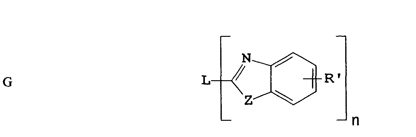
Benzazole derivatives (Formula G) constitute another class of
useful hosts capable of supporting electroluminescence, and are particularly
suitable for light emission of wavelengths longer than 400 nm, for example, blue,
green, yellow, orange or red.
where:
An example of a useful benzazole is 2, 2', 2"-(1,3,5-phenylene)tris[1-phenyl-1H-benzimidazole].
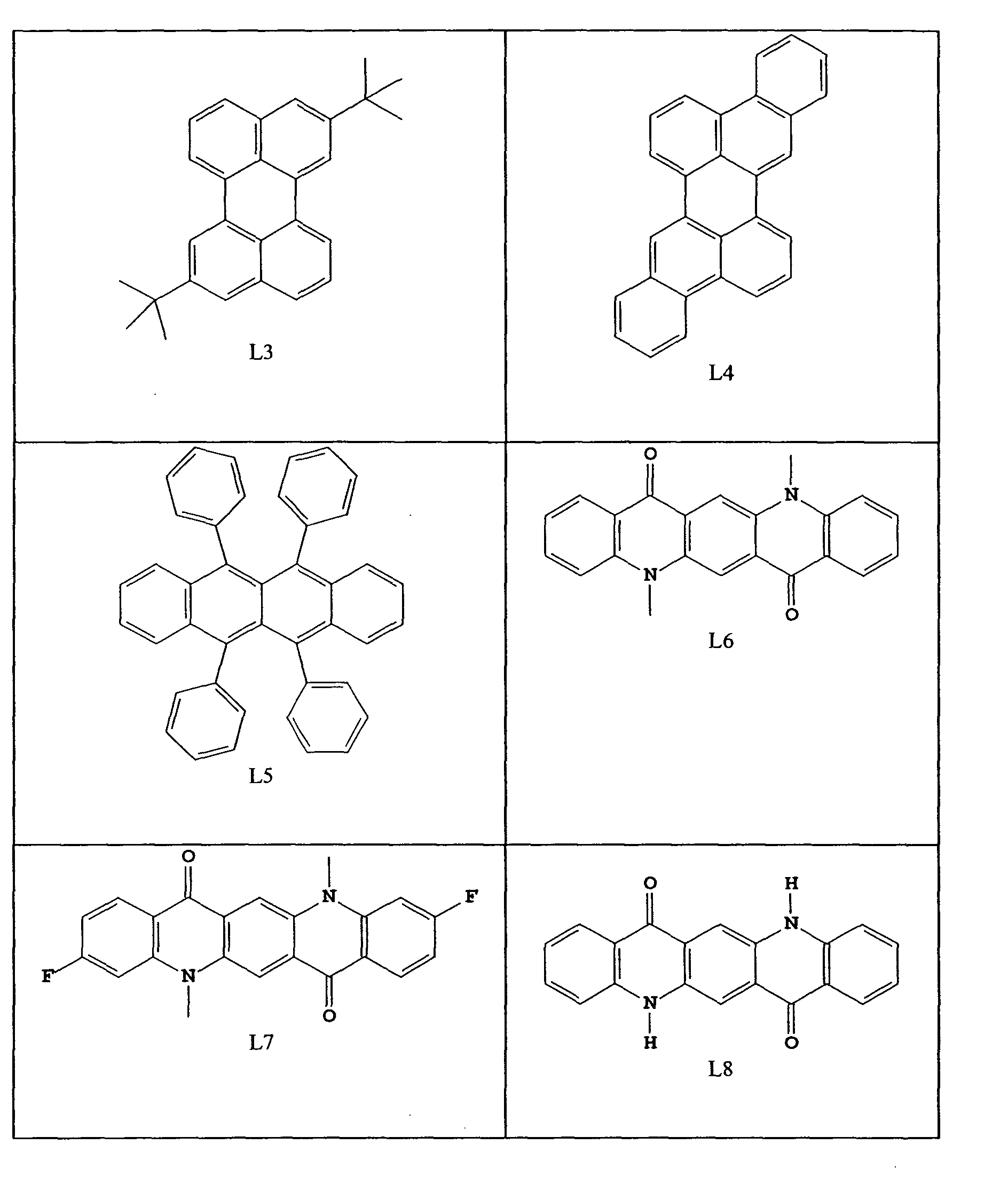
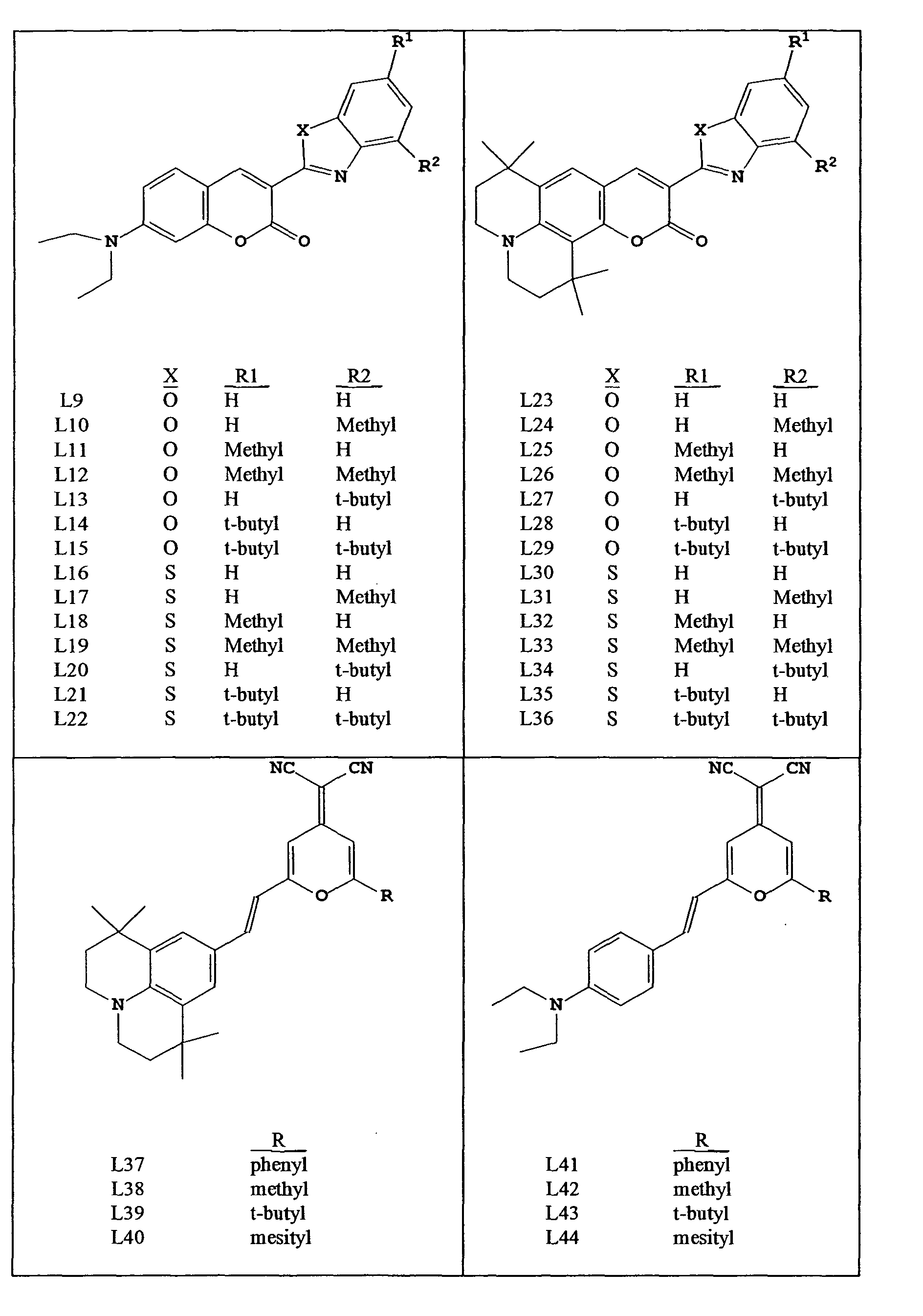
Desirable fluorescent dopants include derivatives of anthracene,
tetracene, xanthene, perylene, rubrene, coumarin, rhodamine, quinacridone,
dicyanomethylenepyran compounds, thiopyran compounds, polymethine
compounds, pyrilium and thiapyrilium compounds, and carbostyryl compounds.
Illustrative examples of useful dopants include, but are not limited to, the
following.
Other organic emissive materials can be polymeric substances, for
example, polyphenylenevinylene derivatives, dialkoxy-polyphenylenevinylenes,
poly-para-phenylene derivatives, and polyfluorene derivatives, as taught by Wolk
and others in commonly assigned US-A-6,194,119 B 1 and references therein.
Donor element 10 can further include other layers, for example a
hole-transporting material or an electron-transporting material as described below,
which is not shown but can be a covering layer over organic emitter layer 18.
Hole-transporting materials are well known to include compounds
such as an aromatic tertiary amine, where the latter is understood to be a
compound containing at least one trivalent nitrogen atom that is bonded only to
carbon atoms, at least one of which is a member of an aromatic ring. In one form
the aromatic tertiary amine can be an arylamine, such as a monoarylamine,
diarylamine, triarylamine, or a polymeric arylamine. Exemplary monomeric
triarylamines are illustrated by Klupfel and others US-A-3,180,730. Other
suitable triarylamines substituted with one or more vinyl radicals and/or
comprising at least one active hydrogen containing group are disclosed by
Brantley and others US-A-3,567,450 and US-A-3,658,520.
A more preferred class of aromatic tertiary amines are those which
include at least two aromatic tertiary amine moieties as described in US-A-4,720,432
and US-A-5,061,569. Such compounds include those represented by
structural Formula (A).
wherein:
In one embodiment, at least one of Q
1 or Q
2 contains a polycyclic fused ring
structure, for example, a naphthalene. When G is an aryl group, it is conveniently
a phenylene, biphenylene, or naphthalene moiety.
A useful class of triarylamines satisfying structural Formula (A)
and containing two triarylamine moieties is represented by structural Formula (B)
where:
wherein R
5 and R
6 are independently selected aryl groups.
In one embodiment, at least one of R
5 or R
6 contains a polycyclic fused ring
structure, for example, a naphthalene.
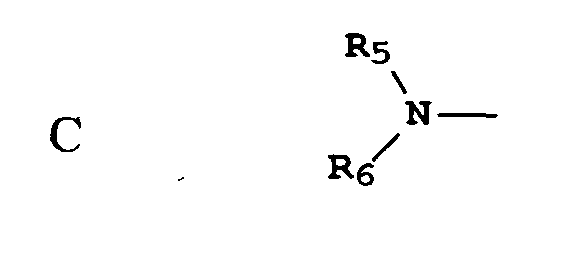
Another class of aromatic tertiary amines is the tetraaryldiamines.
Desirable tetraaryldiamines include two diarylamino groups, such as indicated by
Formula (C), linked through an arylene group. Useful tetraaryldiamines include
those represented by Formula (D).
wherein:
In a typical embodiment, at least one of Ar, R7, R8, and R9 is a
polycyclic fused ring structure, for example, a naphthalene.
The various alkyl, alkylene, aryl, and arylene moieties of the
foregoing structural Formulae (A), (B), (C), (D), can each in turn be substituted.
Typical substituents include alkyl groups, alkoxy groups, aryl groups, aryloxy
groups, and halogen such as fluoride, chloride, and bromide. The various alkyl
and alkylene moieties typically contain from about 1 to 6 carbon atoms. The
cycloalkyl moieties can contain from 3 to about 10 carbon atoms, but typically
contain five, six, or seven ring carbon atoms-for example, cyclopentyl,
cyclohexyl, and cycloheptyl ring structures. The aryl and arylene moieties are
usually phenyl and phenylene moieties.
The hole-transporting layer can be formed of a single or a mixture
of aromatic tertiary amine compounds. Specifically, one can employ a
triarylamine, such as a triarylamine satisfying the Formula (B), in combination
with a tetraaryldiamine, such as indicated by Formula (D). When a triarylamine
is employed in combination with a tetraaryldiamine, the latter is positioned as a
layer interposed between the triarylamine and the electron injecting and
transporting layer. Illustrative of useful aromatic tertiary amines is the following:
Another class of useful hole-transporting materials includes
polycyclic aromatic compounds as described in EP 1 009 041. Tertiary aromatic
amines with more than two amine groups can be used including oligomeric
materials. In addition, polymeric hole-transporting materials can be used such as
poly(N-vinylcarbazole) (PVK), polythiophenes, polypyrrole, polyaniline, and
copolymers such as poly(3,4-ethylenedioxythiophene)/poly(4-styrenesulfonate)
also called PEDOT/PSS.
FIG. 2a shows a cross-sectional representation of a method for
depositing an organic emitter layer 18 from donor element 10 onto portions of
substrate 36 across a minimum gap by treatment with light in the process of
making an OLED device. Substrate 36 can be an organic solid, an inorganic
solid, or a combination of organic and inorganic solids that provides a surface for
receiving the emissive material from a donor. Substrate 36 can be rigid or
flexible and can be processed as separate individual pieces, such as sheets or
wafers, or as a continuous roll. Typical substrate materials include glass, plastic,
metal, ceramic, semiconductor, metal oxide, semiconductor oxide, semiconductor
nitride, or combinations thereof. Substrate 36 can be a homogeneous mixture of
materials, a composite of materials, or multiple layers of materials. Substrate 36
can be an OLED substrate, that is a substrate commonly used for preparing OLED
devices, for example, active-matrix low-temperature polysilicon TFT substrate.
The substrate 36 can either be light-transmissive or opaque, depending on the
intended direction of light emission. The light-transmissive property is desirable
for viewing the EL emission through the substrate. Transparent glass or plastic is
commonly employed in such cases. For applications where the EL emission is
viewed through the top electrode, the transmissive characteristic of the bottom
support is immaterial, and therefore can be light-transmissive, light-absorbing or
light reflective. Substrates for use in this case include, but are not limited to,
glass, plastic, semiconductor materials, ceramics, and circuit board materials, or
any others commonly used in the formation of OLED devices, which can be either
passive-matrix devices or active-matrix devices. Substrate 36 can be coated with
other layers prior to this step.
Coated side 34 of donor element 10 has been positioned in a
material transferring relationship relative to substrate 36. By material transferring
relationship, we mean that donor element 10 and substrate 36 are positioned in a
way to facilitate the transfer of organic emitter from organic emitter layer 18 to
substrate 36. Coated side 34 of donor element 10 is positioned at a predetermined
distance 44 relative to the top of an anode, or the top of a top layer coated over an
anode, on thin-film transistor 40. Predetermined distance can be provided in a
number of ways. In FIG. 2a, predetermined distance 44 is provided by the
structure of substrate 36. The predetermined distance can also be provided by the
structure of donor element 10, for example, by the addition of spacer beads to the
surface of donor element 10, as described by Boroson and others in commonly
assigned US-A-5,714,301.
Donor element 10 has been prepared with radiation-absorbing layer
16 and predetermined distance 44 is maintained by the structure of thin-film
transistors 40 and intervening raised surface portions 42. It is understood that in
other embodiments, predetermined distance 44 can be maintained in other ways,
for example, by the use of spacer elements on coated side 34 of donor element 10,
as taught in commonly assigned U.S. Patent Application Serial No. 10/060,837
filed January 30, 2002 by Mitchell S. Burberry and others, entitled "Using Spacer
Elements to Make Electroluminescent Display Devices", the disclosure of which
is incorporated herein by reference. The gap of a predetermined distance is
maintained in an environment of reduced pressure wherein the mean free path is
larger than the predetermined distance. This means that material crossing the gap
will have a low probability of colliding with any residual gases. In general, this
means a pressure of 1 Torr or less. A pattern of laser light 48 illuminates non-transfer
surface 32 of donor element 10. A large portion of the laser light 48
impinging on radiation-absorbing layer 16 of donor element 10 will be converted
to heat 50, but this will only happen at selectively irradiated portions of donor
element 10. This heats organic emitter layer 18 of donor element 10 in the
immediate vicinity of laser light 48. Some or all of the heated portion of organic
emitter layer 18 transfers by vaporization transport to form organic emitter layer
64 onto receiving surface 46 of organic light-emitting device substrate 36 in a
patterned transfer. Vaporization transport is defined as the process whereby
material is transported across a gap whether it is as individual molecules or small
clusters of molecules. This can include processes such as sublimation,
vaporization, and ablation. Organic emitter layer 18 is drawn for clarity as a
single layer, but it will be understood that it can represent a multilayer coating as
described herein.
FIG. 2b shows a cross-sectional representation of a method for
depositing an organic emitter layer 18 from donor element 10 onto portions of
substrate 36 across a larger gap by treatment with light in the process of making
an OLED device. In this embodiment, predetermined distance 54 is maintained
by spacer elements 58 and by predetermined distance 44 from the structure of
thin-film transistors 40. The gap is maintained in an environment of reduced
pressure wherein the mean free path is larger than the predetermined distance.
This means that material crossing the gap will have a low probability of colliding
with any residual gases. In general, this means a pressure of 1 Torr or less. A
pattern of laser light 48 illuminates non-transfer surface 32. Heat 50 is produced
when laser light 48 strikes radiation-absorbing layer 16. This heats organic
emitter layer 18 in the immediate vicinity of laser light 48. Some or all of the
heated portion of organic emitter layer 18 transfers by vaporization transport to
form organic emitter layer 64 on receiving surface 46 of substrate 36 in a
patterned transfer. Organic emitter layer 18 is drawn for clarity as a single layer,
but it will be understood that it can represent a multilayer coating as described
herein.
FIG. 3 shows an OLED device prepared in accordance with the
method of this invention. OLED device 70 includes anode 62 and cathode 68.
OLED device 70 also includes organic emitter layer 64 and electron-transporting
layer 66. Electron-transporting layer 66 is disposed between cathode 68 and
organic emitter layer 64.
The conductive anode layer is commonly formed over the substrate
and, when EL emission is viewed through the anode, should be transparent or
substantially transparent to the emission of interest. Common transparent anode
materials used in this invention are indium-tin oxide (ITO), indium-zinc oxide
(IZO), and tin oxide, but other metal oxides can work including, but not limited
to, aluminum- or indium-doped zinc oxide, magnesium-indium oxide, and nickel-tungsten
oxide. In addition to these oxides, metal nitrides, such as gallium nitride,
and metal selenides, such as zinc selenide, and metal sulfides, such as zinc sulfide,
can be used as an anode material. For applications where EL emission is viewed
through the top electrode, the transmissive characteristics of the anode material
are immaterial and any conductive material can be used, transparent, opaque or
reflective. Example conductors for this application include, but are not limited to,
gold, iridium, molybdenum, palladium, and platinum. Typical anode materials,
transmissive or otherwise, have a work function of 4.1 eV or greater. Desired
anode materials can be deposited by any suitable means such as evaporation,
sputtering, chemical vapor deposition, or electrochemical means. Anode
materials can be patterned using well known photolithographic processes.
Optionally, anodes can be polished prior to application of other layers to reduce
surface roughness so as to minimize shorts or enhance reflectivity.
When light emission is through the anode, the cathode material can
be comprised of nearly any conductive material. Desirable materials have good
film-forming properties to ensure good contact with the underlying organic layer,
promote electron injection at low voltage, and have good stability. Useful
cathode materials often contain a low work function metal (< 4.0 eV) or metal
alloy. One preferred cathode material is comprised of a Mg:Ag alloy wherein the
percentage of silver is in the range of 1 to 20%, as described in US-A-4,885,221.
Another suitable class of cathode materials includes bilayers comprised of a thin
layer of a low work function metal or metal salt capped with a thicker layer of
conductive metal. One such cathode is comprised of a thin layer of LiF followed
by a thicker layer of A1 as described in US-A-5,677,572. Other useful cathode
materials include, but are not limited to, those disclosed in US-A-5,059,861; US-A-5,059,862;
and US-A-6,140,763.
When light emission is viewed through the cathode, the cathode
must be transparent or nearly transparent. For such applications, metals must be
thin or one must use transparent conductive oxides, or a combination of these
materials. Optically transparent cathodes have been described in more detail in
US-A-4,885,211 and US-A-5,247,190; JP 3,234,963; US-A-5,703,436; US-A-5,608,287;
US-A-5,837,391; US-A-5,677,572; US-A-5,776,622; US-A-5,776,623;
US-A-5,714,838; US-A-5,969,474; US-A-5,739,545; US-A-5,981,306;
US-A-6,137,223; US-A-6,140,763; US-A-6,172,459; EP 1 076 368;
US-A-6,278,236 and US-A-6,284,393. Cathode materials can be deposited by
evaporation, sputtering, or chemical vapor deposition. When needed, patterning
can be achieved through many well known methods including, but not limited to,
through-mask deposition, integral shadow masking as described in US-A-5,276,380
and EP 0 732 868, laser ablation, and selective chemical vapor
deposition.
Preferred electron-transporting materials for use in electron-transporting
layer 66 of this invention are metal chelated oxinoid compounds,
including chelates of oxine itself (also commonly referred to as 8-quinolinol or
8-hydroxyquinoline). Such compounds help to inject and transport electrons and
exhibit both high levels of performance and are readily fabricated in the form of
thin films. Exemplary of contemplated oxinoid compounds are those satisfying
structural Formula (E), previously described.
Other electron-transporting materials include various butadiene
derivatives as disclosed in US-A-4,356,429 and various heterocyclic optical
brighteners as described in US-A-4,539,507. Benzazoles satisfying structural
Formula (G) are also useful electron transporting materials. Triazines are also
known to be useful as electron transporting materials.
Other electron-transport materials can be polymeric substances, for
example, polyphenylenevinylene derivatives, poly-para-phenylene derivatives,
polyfluorene derivatives, polythiophenes, polyacetylenes, and other conductive
polymeric organic materials such as those listed in commonly assigned US-A-6,221,553
B1 and references therein.
In some instances, a single layer can serve the function of
supporting both light emission and electron transportation, and will therefore
include emissive material and electron transport material.
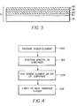
Turning now to FIG. 4, there is shown a block diagram showing
the overall steps in a method for depositing an organic emitter layer onto a
substrate in the process of making an OLED device in accordance with this
invention. First, a donor element 10 is prepared (Step 200). A spacer element or
elements 58 is/are placed on substrate 36 (Step 202). Donor element 10 is then
placed on top of spacer elements 58 (Step 204). Laser light 48 is then used to
effect light-to-heat-induced transfer of organic emitter layer 18 from donor
element 10 to substrate 36 (Step 206). This process is explained in greater detail
in the Examples that follow.
The invention and its advantages can be better appreciated by the
following comparative Examples.
Donor Element Example 1 (Blue donor element)
A donor element satisfying the requirements of the invention was
constructed in the following manner:
Donor Element Example 2 (Red donor element)
A donor element satisfying the requirements of the invention was
constructed in the manner described for donor element Example 1, except step 2
was as follows:
Donor Element Example 3 (Green donor element)
A donor element satisfying the requirements of the invention was
constructed in the manner described for donor element Example 1, except step 2
was as follows:
OLED Device Example 1
A comparative OLED device was constructed in the following
manner:
OLED Device Example 2
An OLED device satisfying the requirements of this invention was
constructed in the manner described for OLED device Example 1 except the
donor element used in step 4 was separated from the NPB layer by 10 micron
shim stock having 2mm x 2mm openings to allow transfer in the electrode area.
OLED Device Examples 3-5
An OLED device satisfying the requirements of this invention was
constructed in the manner described for OLED device Example 2 except the shim
stock used had thickness of 25 microns, 68 microns, and 125 microns,
respectively.
OLED Device Example 6
An evaporative comparative OLED device was constructed in the
following manner:
OLED Device Example 7
An evaporative comparative OLED device was constructed in the
manner described for OLED device Example 6 except the substrate used in step 1
was an OLED substrate having 1 micron photoresist wells in the electrode area.
Device testing consisted of putting a constant current of 20 mA
through the constructed OLED devices with a programmable current source. The
light output was monitored with a Photo Research PR650 spectrophotometer.
Initial radiance and CIE color coordinates x and y were recorded. Device testing
also consisted of putting a constant current through the constructed OLED devices
and recording micrograph of electroluminescence obtained to determine transfer
uniformity. Devices transferred with zero gap exhibited non-uniformities
consisting of interference-like fringes in the luminescence pattern. These patterns
were judged to be strong, medium, or none. The results are shown in Table 1.
| Example # | Example Type | Gap | CIE X | CIE Y | Fringing artifact |
| 1 | Comparative | 0 | 0.184 | 0.274 | S |
| 2 | Invention | 10 | 0.175 | 0.264 | N |
| 3 | Invention | 25 | 0.174 | 0.260 | N |
| 4 | Invention | 68 | 0.171 | 0.248 | N |
| 5 | Invention | 125 | 0.168 | 0.243 | N |
| 6 | Evaporative comparative | ― | 0.160 | 0.251 | N |
| 7 | Evaporative comparative | ― | 0.145 | 0.202 | N |
| * S = Strong fringing pattern, M = medium fringing, N = no fringing |
A comparative OLED device was constructed in the manner
described for OLED device Example 1 except the donor element prepared in
donor element Example 2 was used in step 4.
OLED Device Example 9
An OLED device satisfying the requirements of this invention was
constructed in the manner described for OLED device Example 8 except the
donor element used in step 4 was separated from the NPB layer by 10 micron
shim stock having 2mm x 2mm openings to allow transfer in the electrode area.
OLED Device Examples 10-12
An OLED device satisfying the requirements of this invention was
constructed in the manner described for OLED device Example 9 except the shim
stock used had thickness of 25 microns, 68 microns, and 125 microns,
respectively.
Device testing consisted of putting a constant current through the
constructed OLED devices and recording micrograph of electroluminescence
obtained to determine transfer uniformity. Devices transferred with zero gap
exhibited non-uniformities consisting of interference-like fringes in the
luminescence pattern. These patterns were judged to be strong, medium, or none.
The results are shown in Table 2.
| Example # | Example Type | Gap | Fringing artifact |
| 8 | Comparative | 0 | S |
| 9 | Invention | 10 | S |
| 10 | Invention | 25 | N |
| 11 | Invention | 68 | N |
| 12 | Invention | 125 | N |
A comparative OLED device was constructed in the manner
described for OLED device Example 1 except the donor element prepared in
donor element Example 3 was used in step 4.
OLED Device Example 14
An OLED device satisfying the requirements of this invention was
constructed in the manner described for OLED device Example 13 except the
donor element used in step 4 was separated from the NPB layer by 10 micron
shim stock having 2mm x 2mm openings to allow transfer in the electrode area.
OLED Device Examples 15-17
An OLED device satisfying the requirements of this invention was
constructed in the manner described for OLED device Example 14 except the
shim stock used had thickness of 25 microns, 68 microns, and 125 microns,
respectively.
Device testing consisted of putting a constant current through the
constructed OLED devices and recording micrograph of electroluminescence
obtained to determine transfer uniformity. Devices transferred with zero gap
exhibited non-uniformities consisting of interference-like fringes in the
luminescence pattern. These patterns were judged to be strong, medium, or none.
The results are shown in Table 3.
| Example # | Example Type | Gap | Fringing artifact |
| 13 | Comparative | 0 | S |
| 14 | Invention | 10 | S |
| 15 | Invention | 25 | M |
| 16 | Invention | 68 | N |
| 17 | Invention | 125 | N |
For blue, color improves as both x and y decrease. The data in
Table 1 show that blue color did improve as the gap increased. This suggests that
selecting a predetermined distance of 4 micrometers or greater can lead to an
improvement in emission spectrum. The predetermined distance can be selected
so that the spectrum of light emitted from the OLED device will be in the desired
emission wavelength. Red and green cells did not change color appreciably with
increasing gap.
Blue, red, and green devices transferred with zero gap exhibited
interference-like fringes in the electroluminescence pattern. These appear to
correspond to the topographical contours reflecting tiny space variations between
the donor and the receiver induced by irregularities. Larger gaps showed
successively less susceptibility to fringing. Gaps greater than 10 microns
exhibited little or no fringing patterns. This suggests that a selecting a
predetermined distance of 25 micrometers or greater can lead to an improvement
in uniformity. An upper limit in predetermined distance is created by dispersion
of organic emitter layer 64 to locations on substrate 36 other than the desired
location. Such upper limit is on the order of 75 micrometers.
The present invention speculates that increasing gap increases the
uniformity of transfer by averaging the spatial distribution and arrival times of
transferred material form different locations on the donor. The laser transfer
process is complex and can effect the emissive layer of different materials in
various ways. Blue emissive cells, for example, are more susceptible to unwanted
green emission because energy transfer to A1Q3 states is exothermic. The
uniformity and morphological changes with increasing gap can effect the
distribution of recombination centers, reducing the unwanted green. Red cells are
less susceptible to unwanted green emission because the energy levels of red
dopants are lower than the green states of Alq3. In green cells emission from the
Alq3 is practically indistinguishable from the green emission layer. In all cells,
red, green and blue, increasing gap produced more uniform emission as observed
in the redetection of fringe-like artifacts in the electroluminescence.
Other features of the invention are included below.
The method wherein the organic emitter has a desired emission
spectrum in the blue region of the visible spectrum.
The method wherein the organic emitter has a desired emission
spectrum in the green region of the visible spectrum.
The method wherein the organic emitter has a desired emission
spectrum in the red region of the visible spectrum.
The method wherein the predetermined distance is provided by the
structure of the donor element.
The method wherein the predetermined distance is provided by the
structure of the substrate.
The method wherein the predetermined distance is provided by
spacer elements.
The method wherein the organic emitter has a desired emission
spectrum in the green region of the visible spectrum.
The method wherein the organic emitter has a desired emission
spectrum in the red region of the visible spectrum.
The method wherein the predetermined distance is provided by the
structure of the donor element.
The method wherein the predetermined distance is provided by the
structure of the substrate.