EP1408538A1 - Polishing element, cmp polishing device and productions method for semiconductor device - Google Patents
Polishing element, cmp polishing device and productions method for semiconductor device Download PDFInfo
- Publication number
- EP1408538A1 EP1408538A1 EP02743826A EP02743826A EP1408538A1 EP 1408538 A1 EP1408538 A1 EP 1408538A1 EP 02743826 A EP02743826 A EP 02743826A EP 02743826 A EP02743826 A EP 02743826A EP 1408538 A1 EP1408538 A1 EP 1408538A1
- Authority
- EP
- European Patent Office
- Prior art keywords
- polishing
- mentioned
- elastic member
- hard elastic
- wafer
- Prior art date
- Legal status (The legal status is an assumption and is not a legal conclusion. Google has not performed a legal analysis and makes no representation as to the accuracy of the status listed.)
- Withdrawn
Links
Images





Classifications
-
- H—ELECTRICITY
- H10—SEMICONDUCTOR DEVICES; ELECTRIC SOLID-STATE DEVICES NOT OTHERWISE PROVIDED FOR
- H10P—GENERIC PROCESSES OR APPARATUS FOR THE MANUFACTURE OR TREATMENT OF DEVICES COVERED BY CLASS H10
- H10P52/00—Grinding, lapping or polishing of wafers, substrates or parts of devices
-
- B—PERFORMING OPERATIONS; TRANSPORTING
- B24—GRINDING; POLISHING
- B24B—MACHINES, DEVICES, OR PROCESSES FOR GRINDING OR POLISHING; DRESSING OR CONDITIONING OF ABRADING SURFACES; FEEDING OF GRINDING, POLISHING, OR LAPPING AGENTS
- B24B37/00—Lapping machines or devices; Accessories
- B24B37/11—Lapping tools
- B24B37/20—Lapping pads for working plane surfaces
-
- B—PERFORMING OPERATIONS; TRANSPORTING
- B24—GRINDING; POLISHING
- B24D—TOOLS FOR GRINDING, BUFFING OR SHARPENING
- B24D13/00—Wheels having flexibly-acting working parts, e.g. buffing wheels; Mountings therefor
- B24D13/20—Mountings for the wheels
-
- H—ELECTRICITY
- H10—SEMICONDUCTOR DEVICES; ELECTRIC SOLID-STATE DEVICES NOT OTHERWISE PROVIDED FOR
- H10P—GENERIC PROCESSES OR APPARATUS FOR THE MANUFACTURE OR TREATMENT OF DEVICES COVERED BY CLASS H10
- H10P52/00—Grinding, lapping or polishing of wafers, substrates or parts of devices
- H10P52/40—Chemomechanical polishing [CMP]
- H10P52/403—Chemomechanical polishing [CMP] of conductive or resistive materials
-
- H—ELECTRICITY
- H10—SEMICONDUCTOR DEVICES; ELECTRIC SOLID-STATE DEVICES NOT OTHERWISE PROVIDED FOR
- H10P—GENERIC PROCESSES OR APPARATUS FOR THE MANUFACTURE OR TREATMENT OF DEVICES COVERED BY CLASS H10
- H10P95/00—Generic processes or apparatus for manufacture or treatments not covered by the other groups of this subclass
- H10P95/06—Planarisation of inorganic insulating materials
- H10P95/062—Planarisation of inorganic insulating materials involving a dielectric removal step
-
- H—ELECTRICITY
- H10—SEMICONDUCTOR DEVICES; ELECTRIC SOLID-STATE DEVICES NOT OTHERWISE PROVIDED FOR
- H10P—GENERIC PROCESSES OR APPARATUS FOR THE MANUFACTURE OR TREATMENT OF DEVICES COVERED BY CLASS H10
- H10P95/00—Generic processes or apparatus for manufacture or treatments not covered by the other groups of this subclass
- H10P95/04—Planarisation of conductive or resistive materials
Definitions
- the present invention relates to a CMP polishing apparatus which is used to polish wafers that have semiconductor integrated circuits formed inside, a polishing body which is used in this CMP polishing apparatus, and a semiconductor device manufacturing method which uses this CMP polishing apparatus.
- the wavelengths of light sources in semiconductor exposure apparatuses used in photolithography have become shorter, and the numerical aperture or so-called NA of the projection lenses used in such semiconductor exposure apparatuses has become larger.
- the focal depth of the projection lenses used in such semiconductor exposure apparatuses has become substantially shallower. In order to deal with such increasing shallowness of the focal depth, there is a demand for even greater planarization of the surfaces of semiconductor devices than that achieved so far.
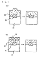
- Figure 9 is a schematic diagram illustrating planarization techniques used in a semiconductor manufacturing process, and shows sectional views of a semiconductor device.
- 31 indicates a silicon wafer
- 32 indicates an inter-layer insulating film consisting of SiO 2
- 33 indicates a metal film consisting of Cu
- 34 indicates the semiconductor device.
- Figure 9 (a) shows an example of the planarization of an inter-layer insulating film 32 on the surface of the semiconductor device.
- Figure 9 (b) shows an example in which a so-called damascene is formed by polishing the metal film 33 on the surface of the semiconductor device.
- a chemical mechanical polishing or chemical mechanical planarization (hereafter referred to as "CMP") technique is widely used as a method for planarizing the surfaces of such semiconductor devices.
- CMP chemical mechanical polishing or chemical mechanical planarization
- CMP was developed on the basis of silicon wafer mirror surface polishing methods, and is performed using a CMP apparatus of the type shown in Figure 10.
- 35 indicates a polishing member
- 36 indicates a member that holds the object of polishing (hereafter referred to as a "polishing head" in some instances)
- 37 indicates a silicon wafer which is the object of polishing
- 38 indicates a polishing agent supply part
- 39 indicates a polishing agent.
- the polishing member 35 has a polishing pad 41 which is attached to the surface of a polishing platen 40.
- a sheet-form foam polyurethane is widely used as such a polishing pad 41.
- the object of polishing 37 is held by the polishing head 36, so that it is caused to oscillate while being rotated, and is pressed against the polishing pad 41 of the polishing member 35 with a specified pressure.
- the polishing member 35 is also rotated, so that a relative motion is performed between the polishing member 35 and the object of polishing 37.
- the polishing agent 39 is supplied to the surface of the polishing pad 41 from the polishing agent supply part 38.
- the polishing agent 39 diffuses over the surface of the polishing pad 41, and enters the space between the polishing pad 41 and the object of polishing 37 as the polishing member 35 and object of polishing 37 move relative to each other, so that the surface of the object of polishing 37 that is to be polished is polished.
- good polishing is accomplished by a synergistic effect of the mechanical polishing caused by the relative motion of the polishing member 35 and object of polishing 37 and the chemical action of the polishing agent 39.
- the surfaces of wafers that have semiconductor integrated circuits formed inside are not flat; in particular, there are usually step differences between portions in which chips are formed and portions in which chips are not formed. Accordingly, in cases where such wafers are polished, there is a need to eliminate local indentations and projections (this is called “local pattern planarity” while polishing the wafer in conformity to large periodic indentations and projections (undulations) of the wafer substrate itself, i.e., uniformly along such indentations and projections (undulations) (this is called “wafer global removal uniformity").
- a method has been developed in which a polishing body is formed by pasting together a polishing pad and a soft pad, and this polishing body is used instead of the polishing pad 41 shown in Figure 10.
- a polishing body 44 is formed by pasting together a polishing pad 42 and a pad 43 which has a low elastic modulus and a large compressive deformation rate, and this polishing body 44 is attached to the polishing platen 40.
- polishing of the type shown in Figure 10 when polishing of the type shown in Figure 10 is performed, the pad 43 is caused to undergo compressive deformation by the force that is applied to the large undulation of the wafer 37 via the polishing pad 42, so that the polishing pad 42 also deforms in conformity to this deformation. Accordingly, polishing can be performed in which the amount of polishing is fixed in accordance with the undulation in the surface of the wafer 37. Meanwhile, in the case of local indentations and projections, the deformation of the polishing pad 42 is relatively small; accordingly, such indentations and projections can be removed by polishing.
- the present invention was devised in order to solve such problems.
- the object of the present invention is to provide a polishing body which can satisfy both the requirements of "wafer global removal uniformity" and the requirements of "local pattern planarity" even in cases where wafers are polished which have patterns that use a wiring rule of 0.1 ⁇ m or less or patterns that have a severe density distribution are formed inside, a CMP polishing apparatus using this polishing body, and a semiconductor device manufacturing method using such a CMP apparatus.
- the first invention of the present application which is used to achieve the above-mentioned object is a polishing body for a CMP polishing apparatus which is used to polish wafers that have semiconductor integrated circuits formed inside, wherein a polishing pad, a hard elastic member and a soft member are laminated in that order, and the above-mentioned hard elastic member is constructed so that the amount of deformation of this member at the polishing load that is applied during polishing is smaller than the step difference permitted in the above-mentioned wafer in an interval corresponding to the maximum pattern of the above-mentioned semiconductor integrated circuits, and is greater than the TTV permitted in the above-mentioned wafer in the interval corresponding to one chip.
- TTV total thickness variation
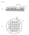
- Figure 1 (a) shows a sectional view of the wafer prior to polishing.
- 1 indicates the wafer substrate
- 2 indicates patterns consisting of circuits and wiring
- 3 indicates an inter-layer insulating layer.
- the patterns 2 consisting of circuits and wiring are formed on the surface of the substrate 1, and the inter-layer insulating layer 3 is formed on top of this, so that the patterns 2 consisting of circuits and wiring are insulated from each other.
- the interval corresponding to the maximum pattern of the semiconductor integrated circuits refers to the interval corresponding to the distance a of the recessed part of the inter-layer insulating film 3 that covers the patterns 2 of circuits and wiring that are most separated from each other within one chip.
- the interval corresponding to the maximum pattern of such semiconductor integrated circuits is approximately 4 mm.
- Figure 1 (b) shows a single wafer, with a plurality of chips 5 being formed on this wafer 1.
- the interval corresponding to one chip refers to the interval corresponding to one side b in a case where the shape of the chip is square. Currently, this interval is approximately 20 mm. In cases where the shape of the chip is not square, or in cases where chips of different dimensions are formed on one wafer, this interval refers to the distance corresponding to the largest side.
- the hard elastic member refers to an elastic member with a Young's modulus of 10,000 Kg/mm 2 or greater; metal members may be cited as typical examples.
- the soft member refers to a member that has a compression rate of 10% or greater when a pressure of 1 Kg/cm 2 is applied; chloroprene rubber members containing air bubbles, or elastic nonwoven fabrics, may be cited as typical examples.
- a hard elastic member is sandwiched between the polishing pad and a soft member. Furthermore, the amount of deformation of this hard elastic member at the load that is applied during polishing is set so that this amount of deformation is smaller than the step difference that is permitted in the above-mentioned wafer in the interval corresponding to the maximum pattern of the above-mentioned semiconductor integrated circuits. Accordingly, since the hard elastic member is not subjected to deformation exceeding the permitted step difference in the interval corresponding to the maximum pattern, "local pattern planarity" is ensured.
- the amount of deformation of the hard elastic member at the polishing load that is applied during polishing is set so that this amount of deformation is greater than the TTV permitted in the wafer in the interval corresponding to one chip. Accordingly, the hard elastic member can deform in conformity to the step difference over the distance corresponding to one chip, and the polishing pad also shows a corresponding deformation in conformity to these step differences, so that a uniform amount of polishing can be performed in accordance with these step differences. Consequently, "wafer global removal uniformity" is ensured.
- the second invention of the present application that is used to achieve the above-mentioned object is the polishing body of the first invention, wherein the above-mentioned hard elastic member is constructed from a metal plate that will not dissolve in the polishing agent.
- the material of the above-described hard elastic member there are no particular stipulations regarding the material of the above-described hard elastic member. Accordingly, a hard plastic or hard rubber, for example, can be used. However, a hard plastic or hard rubber, etc., has a small Young's modulus; accordingly, if such a material is used in the above-described first invention, the thickness of the member must be set at a large value. If this thickness is increased, the degree of parallel orientation of the two surfaces deteriorates; furthermore, irregularities in thermal expansion occur as a result of temperature irregularities caused by the heat generated during polishing, and such irregularities cause a deterioration in planarity.
- the above-described hard elastic member is formed from a metal, the Young's modulus of the hard elastic member is high; accordingly, the thickness of this member can be reduced. Consequently, the degree of parallel orientation of the two surfaces can be maintained at a favorable value, and irregularities in thermal expansion can be reduced, so that the planarity can be maintained at a favorable value. Furthermore, the reason that the type of metal used is limited to a metal that will not dissolve in the polishing agent is as follows: specifically, if the metal dissolves in the polishing agent, there may be cases in which this has a deleterious effect on the semiconductor integrated circuits that are formed on the wafer. Stainless steel and titanium may be cited as examples of metals that will not dissolve in commonly used polishing agents.
- the third invention of the present application that is used to achieve the above-mentioned object is the polishing body of the above-mentioned second invention, wherein the above-mentioned metal plate is a stainless steel plate, and the thickness h of this plate is such that 0.1 mm ⁇ h ⁇ 0.94 mm.
- the effect described in the above-mentioned first means can be obtained; furthermore, the effect described in the above-mentioned second means can also be obtained.
- a stainless steel plate is readily available, and is less expensive than other materials.
- a stainless steel thickness h which is such that 0.1 mm ⁇ h ⁇ 0.94 mm satisfies the conditions fixed by the above-mentioned first invention at a surface pressure of 100 g/cm 2 to 700 g/cm 2 . Accordingly, in the present invention, the thickness of the stainless steel is limited as described above.
- the fourth invention of the present application that is used to achieve the above-mentioned object is a polishing body for a CMP polishing apparatus which is used to polish wafers that have semiconductor integrated circuits formed inside, wherein a polishing pad, a hard elastic member and a soft member are laminated in that order, and these parts are constructed so that the combined amount of deformation of the polishing pad, hard elastic member and soft member at the polishing load that is applied during polishing is smaller than the height of the indentations and projections of the above-mentioned maximum pattern in the interval corresponding to the maximum pattern of the above-mentioned semiconductor integrated circuits, and is greater than five times the TTV that is permitted in the above-mentioned wafer.
- a hard elastic member is sandwiched between the polishing pad and a soft member. Furthermore, the combined amount of deformation of the polishing pad, hard elastic member and soft member at the polishing load that is applied during polishing is smaller than the height of the indentations and projections of the above-mentioned maximum pattern in the interval corresponding to the maximum pattern of the above-mentioned semiconductor integrated circuits. Accordingly, since the polishing body is not subjected to deformation exceeding the height of the indentations and projections of the maximum pattern in the interval corresponding to the maximum pattern, the step difference between patterns following polishing can be suppressed to a difference that is less than the height of the indentations and projections of the maximum pattern. Consequently, "local pattern planarity" is ensured.
- the combined amount of deformation of the polishing pad, hard elastic member and soft member at the polishing load that is applied during polishing is set so that this amount of deformation is greater than five times the TTV that is permitted in the wafer in the interval corresponding to one chip.
- the amount of deformation of the polishing body must be five times the required TTV or greater if "wafer global removal uniformity" is to be obtained.
- the polishing pad As a result of the combined amount of deformation of the polishing pad, hard elastic member and soft member being set so that this amount of deformation is greater than five times the TTV that is permitted in the wafer in the interval corresponding to one chip, the polishing pad also deforms in conformity to the step differences in cases where there are step differences in the distance corresponding to one chip. Accordingly, a uniform amount of polishing can be performed in accordance with these step differences. Consequently, "wafer global removal uniformity" is ensured.
- the fifth invention of the present application that is used to achieve the above-mentioned object is the polishing body of the above-mentioned fourth invention, wherein the above-mentioned hard elastic member is constructed from a metal plate that will not dissolve in the polishing agent.
- the material of the above-mentioned hard elastic member there are no particular stipulations regarding the material of the above-mentioned hard elastic member. Accordingly, a hard plastic or hard rubber, for example, can be used. However, since hard plastics and hard rubbers, etc., have a small Young's modulus, the thickness must be increased if such materials are used in the above-mentioned fourth means. When the thickness increases, the degree of parallel orientation of the two surfaces deteriorates; furthermore, irregularities in thermal expansion occur as a result of temperature irregularities caused by the heat generated during polishing, and such irregularities cause a deterioration in planarity.
- the Young's modulus is high; accordingly, the thickness of the member can be reduced. Consequently, the degree of parallel orientation of the two surfaces can be maintained at a favorable value, and irregularities in thermal expansion can also be reduced, so that the planarity can be maintained at a favorable value.
- the reason that the type of metal used is limited to a metal that will not dissolve in the polishing agent is as follows: specifically, if the metal dissolves in the polishing agent, there are cases in which this has a deleterious effect on the semiconductor integrated circuits that are formed on the wafer. Examples of metals that will not dissolve in commonly used polishing agents include stainless steel and titanium.
- the sixth invention of the present application that is used to achieve the above-mentioned object is the polishing body of the fifth invention, wherein the above-mentioned polishing pad consists of a urethane foam material, the above-mentioned metal plate is a stainless steel plate, the thickness of the above-mentioned polishing pad is 0.1 to 3 mm, the thickness of the above-mentioned metal body is 0.05 to 0.6 mm, and the thickness of the above-mentioned soft member is 0.5 to 2.5 mm.
- the above-mentioned polishing pad consists of a urethane foam material
- the above-mentioned metal plate is a stainless steel plate
- the thickness of the above-mentioned polishing pad is 0.1 to 3 mm
- the thickness of the above-mentioned metal body is 0.05 to 0.6 mm
- the thickness of the above-mentioned soft member is 0.5 to 2.5 mm.
- a urethane foam material is superior as the material of a polishing pad; furthermore, a stainless steel plate is easy to obtain, and is less expensive than other materials. In cases where such materials are used, as will be described in the embodiments later, the requirements of both "wafer global removal uniformity" and “local pattern planarity” can be satisfied under advantageous conditions by setting the thicknesses of the polishing pad, metal plate and soft member as described above.
- the thickness of the polishing pad is less than 0.1 mm, the grooves used to conduct the slurry, which are ordinarily formed in the polishing pad, are eliminated. Accordingly, in the present means, the thickness of the polishing pad is limited to a thickness of 0.1 mm or greater. Furthermore, even if the thickness of the polishing pad exceeds 3 mm, no particular advantage is gained, and there is no great difference between such a polishing body and a polishing body in which no metal plate is sandwiched between the other parts as described above; accordingly, in the present means, the thickness of the polishing pad is limited to a thickness of 3 mm or less.
- the thickness of the metal body is limited to a thickness of 0.05 mm or greater.
- the thickness of the metal body exceeds 0.6 mm, the limiting conditions of the above-mentioned fourth invention cannot be realized in the case of a wafer with a TTV of 1 ⁇ m; accordingly, in the present means, the thickness of the metal body is limited to a thickness of 0.6 mm or less.
- the thickness of the soft member does not greatly affect the "wafer global removal uniformity" or "local pattern planarity.”
- an experiment (simulation) for the purpose of deriving the limits on the above-mentioned respective numerical values in the present invention was conducted in the range of 0.5 to 2.5 mm, the thickness is limited to this range.
- the seventh invention of the present application that is used to achieve the above-mentioned object is the polishing body of any of the above-mentioned first through sixth inventions, wherein the above-mentioned soft member has a torsional strength which is such that this member is not damaged when the member rotates with a load applied during polishing.
- the above-mentioned soft member has a torsional strength which is such that this member is not damaged when the member rotates with a load applied during polishing; accordingly, polishing can be performed smoothly.
- the eighth invention of the present application that is used to achieve the above-mentioned object is the polishing body of any of the above-mentioned first through seventh inventions, wherein the above-mentioned hard elastic member and soft member are fastened by bonding, and the above-mentioned hard elastic member and polishing pad are fastened by vacuum suction.
- the polishing pad since the hard elastic member and polishing pad are fastened by vacuum suction, the polishing pad can easily be replaced when the polishing pad becomes worn.
- the ninth invention of the present application that is used to achieve the above-mentioned object is the polishing body of any of the above-mentioned first through seventh inventions, wherein the above-mentioned hard elastic member and soft member are fastened by bonding means with a strong peeling strength, and the above-mentioned hard elastic member and polishing pad are fastened by bonding means with a weak peeling strength.
- the polishing pad can be peeled from the hard elastic member in a state in which the hard elastic member and soft member remain bonded. Accordingly, the polishing pad can easily be replaced when the polishing pad becomes worn.
- the tenth invention of the present application that is used to achieve the above-mentioned object is a CMP polishing apparatus which is used to polish wafers that have semiconductor integrated circuits formed inside, and which has the polishing body of any of the above-mentioned first through ninth inventions.
- the eleventh invention of the present application that is used to achieve the above-mentioned object is a CMP polishing apparatus which is used to polish wafers that have semiconductor integrated circuits formed inside, and which has the polishing body of the above-mentioned eighth or ninth invention, wherein the dimensions of the above-mentioned polishing pad are set so that these dimensions are smaller than the dimensions of the wafer that is being polished.
- CMP polishing apparatuses There are two types of CMP polishing apparatuses, i.e., apparatuses in which the dimensions of the polishing pad are larger than the dimensions of the wafer that is being polished, and apparatuses in which the dimensions of the polishing pad are smaller than the dimensions of the wafer that is being polished.
- the polishing body of the above-mentioned eighth or ninth invention is used in the latter type of apparatus. Accordingly, since the size of the polishing body pad is small, attachment by vacuum suction can easily be accomplished, so that the polishing pad can be securely fastened to the hard elastic member. Furthermore, in such a CMP apparatus, since the polishing pad is small, frequent replacement of the polishing pad is necessary. Accordingly, an especially great effect is obtained by using the polishing body of the above-mentioned eighth or ninth invention, in which replacement of the polishing pad is easy.
- the twelfth invention of the present application that is used to achieve the above-mentioned object is a CMP polishing apparatus which is used to polish wafers that have semiconductor integrated circuits formed inside, and which has the polishing body of the above-mentioned seventh invention, wherein the dimensions of the above-mentioned polishing pad are set so that these dimensions are smaller than the dimensions of the wafer that is being polished, and the permissible shear stress of the above-mentioned soft member is greater than 0.5 Kg/cm 2 .
- the above-mentioned soft member can be endowed with a torsional strength which is such the member is not damaged when the member rotates with a load applied during polishing, by setting the permissible shear stress of the above-mentioned soft member at a value that is greater than 0.5 Kg/cm 2 .
- the thirteenth invention of the present application that is used to achieve the above-mentioned object is a semiconductor device manufacturing method which is characterized in that this method has a process in which the polishing of wafers is performed using the CMP polishing apparatus of any of the abovementioned tenth through twelfth inventions.
- wafers can be polished while satisfying the requirements of both "wafer global removal uniformity" and "local pattern planarity,” which are required in the polishing of wafers that have semiconductor devices formed inside. Accordingly, a semiconductor exposure apparatus which has a shallow focal depth can be used, and semiconductor devices that have fine patterns can be manufactured with a good yield.
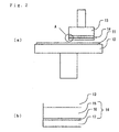
- Figure 2 (a) is a diagram which shows an outline of a CMP polishing apparatus and a polishing body constituting one example of a working configuration of the present invention.
- Figure 2 (b) is an enlarged view of the portion labeled A in Figure 2 (a). In this working configuration, the size of the polishing pad is smaller than the size of the wafer, unlike the case of the conventional CMP apparatus shown in Figure 10.
- the wafer 11 that is the object of polishing is held by a polishing head 12, and rotates together with the polishing head 12.
- a polishing body 14 is attached to the polishing member 13 by bonding using an adhesive agent or two-sided adhesive tape, etc.
- the polishing body 14 is constructed by laminating a soft member 15, a hard elastic member 16 and a polishing pad 17. In this working configuration, the soft member 15, hard elastic member 16 and polishing pad 17 are bonded by means of an adhesive agent or two-sided adhesive tape, etc.
- the polishing body 14 rotates together with the polishing member 13, and swings at the same time; as a result, the polishing pad 17 polishes the entire surface of the wafer 11.
- a polishing agent is supplied to the area between the wafer 11 and the polishing pad 17; however, this is not shown in the figures.
- the thickness of the hard elastic member 16 is determined so that the amount of deformation of the hard elastic member 16 caused by the load during polishing is smaller than the step difference that is permitted in the wafer in the interval corresponding to the maximum pattern of the semiconductor integrated circuits, and is larger than the TTV that is permitted in the wafer in the interval corresponding to one chip.
- the thickness h that satisfies the above-mentioned conditions is a thickness which is such that 0.20 mm ⁇ h ⁇ 0.62 mm. If a hard plastic with a Young's modulus E of 400 Kg/mm 2 is used instead of stainless steel, the thickness h is such that 0.74 mm ⁇ h ⁇ 2.32 mm. If the thickness is too great, there are many inconveniences as described above; accordingly, it is desirable to use a metal which allows a small thickness as the hard elastic member.
- Table 1 shows the relationship between the surface pressure during polishing and the limiting conditions on the thickness h in a cases where stainless steel is used as the material of the hard elastic member 16.
- the permitted step difference in the case of a 0.35 ⁇ m wiring rule is set at 0.35 ⁇ m, and the TTV is set at 5 ⁇ m.
- a member which has a large compressive deformation and which tends not to undergo plastic deformation is desirable to use as the soft member 15.
- a chloroprene rubber, etc., which has air bubbles inside can be used as the material of this member.
- this material have a torsional strength which is such that the member is not damaged when the member rotates with a load applied during polishing.
- the polishing pad 17 will conform to large undulations corresponding to one chip, so that polishing in which the amount of polishing is fixed can be performed, with the polishing pad 17 showing almost no deformation in the case of local indentations and projections with a spacing corresponding to the maximum spacing of the wiring pattern; accordingly, the requirements of both "wafer global removal uniformity" and "local pattern planarity" can be satisfied.
- stainless steel can be used as the material of the hard elastic member 16, and the thicknesses of the respective members can be determined so that the combined deformation of the polishing pad 17, hard elastic member 16 and soft member 15 caused by the load during polishing is smaller than the height of the indentations and projections of the maximum pattern in the interval corresponding to the maximum pattern of the semiconductor integrated circuits, and greater than five times the TTV permitted in the wafer in the interval corresponding to one chip in this working configuration.
- a member which shows a large compressive deformation and which tends not to undergo plastic deformation is desirable as the soft member 15.
- a chloroprene rubber which has air bubbles inside, or an elastic nonwoven fabric, etc. can be used.
- the polishing pad 17 will conform to large undulations corresponding to one chip, so that polishing in which the amount of polishing is fixed can be performed, with the polishing body 14 showing almost no deformation in the case of local indentations and projections with a spacing corresponding to the maximum spacing of the wiring pattern; accordingly, the requirements of both "wafer global removal uniformity" and "local pattern planarity" can be satisfied.
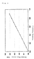
- the graph in Figure 3 shows the results obtained when the relationship between the surface pressure (polishing pressure) p (kg/cm 2 ) and the maximum shear stress ⁇ max (kg/cm 2 ) was determined by calculation in a cases where a polishing pad with an external diameter D of 170 mm and an internal diameter d of 60 mm was used in the CMP polishing apparatus shown in Figure 2, and the coefficient of friction k was 0.35.
- the soft member 15 in a CMP polishing apparatus of the type shown in Figure 2, can be endowed with a torsional strength which is such that the soft member 15 is not damaged under ordinary polishing conditions (polishing pressure: 1.0 Kg/cm 2 ) if the maximum shear stress ⁇ max permitted in the soft member 15 is greater than 0.5 Kg/cm 2 .
- Figure 4 shows an outline (sectional view) of a polishing body constituting another working configuration of the present invention.
- constituent elements that are the same as constituent elements shown in Figure 2 are labeled with the same symbols, and a description of such elements is omitted.
- the working configuration shown in Figure 4 as well, the basic construction and the materials of the soft member 15, hard elastic member 16 and polishing pad 17 are the same as those shown in Figure 1.
- the soft member 15 is bonded to the polishing member 13 by an adhesive agent or two-sided adhesive tape
- the hard elastic member 16 is bonded to the soft member 15 by an adhesive tape or two-sided adhesive tape.
- the hard elastic member 16 and the polishing pad 17 are not bonded.
- holes 18 are formed which pass through the polishing member 13, soft member 15 and hard elastic member 16, and the polishing pad 17 is fastened to the hard elastic member 16 through vacuum suction by setting the pressure inside these holes 18 at a low pressure that is close to a vacuum in a state in which the polishing pad 17 is pressed against the hard elastic member 16.
- the polishing pad 17 can easily be removed merely by releasing the vacuum state in cases where the polishing pad 17 is to be replaced as a result of wear, so that replacement is easy.
- the number of holes 18 required is small, so that a vacuum suction mechanism can easily be provided; accordingly, such a construction is effective.
- the frequency of replacement is high; accordingly, the construction shown in Figure 4 is effective in this respect as well.
- the polishing pad 17 can easily be peeled from the hard elastic member 16 by using bonding means with a strong peeling strength between the polishing member 13 and soft member 15 and between the soft member 15 and hard elastic member 16, and using bonding means with a weak peeling strength between the hard elastic member 16 and polishing pad 17.
- bonding means with a strong peeling strength between the polishing member 13 and soft member 15 and between the soft member 15 and hard elastic member 16
- bonding means with a weak peeling strength between the hard elastic member 16 and polishing pad 17.
- the worn polishing pad 17 can easily be replaced in the same manner as in the above-mentioned working configuration in which a vacuum suction attachment mechanism was provided.
- the 180° peeling adhesive strength of the adhesive layers between the polishing member 13 and soft member 15 and between the soft member 15 and the hard elastic member 16 be greater than 1500 g/25 mm, and that the 180° peeling adhesive strength of the adhesive layer between the hard elastic member 16 and the polishing pad 17 be smaller than 1000 g/25 mm.
- FIG. 5 is a flow chart which shows a semiconductor device manufacturing process constituting one example of a working configuration of the present invention. After the semiconductor device manufacturing process is started, the appropriate processing step is first selected in step S100 from the steps S101 through S104 described below. In accordance with this selection, the processing proceeds to one of the steps S101 through S104.
- Step S101 is an oxidation step in which the surface of the silicon wafer is oxidized.
- Step S102 is a CVD step in which an insulating film is formed on the surface of the silicon wafer by CVD, etc.
- Step S103 is an electrode formation step in which electrodes are formed on the silicon wafer by a process such as vacuum evaporation.
- Step S104 is an ion injection step in which ions are injected into the silicon wafer.
- step S105 a judgement is made as to whether or not a CMP process is to be performed, and in cases where such a process is to be performed, the processing proceeds to the CMP process of step S106. In cases where a CMP process is not to be performed, step S106 is bypassed.
- the CMP process the flattening of inter-layer insulation films, or the formation of a damascene by the polishing of metal films on the surfaces of semiconductor devices, etc., is performed using the polishing apparatus of the present invention.
- Step S107 is a photolithographic step.
- the silicon wafer is coated with a resist, circuit patterns are burned onto the silicon wafer by exposure using an exposure apparatus, and the exposed silicon wafer is developed.
- the next step S108 is an etching step in which the portions other than the developed resist image are removed by etching, the resist is then peeled away, and the resist that has become unnecessary following etching is removed.
- step S109 a judgement is made as to whether or not all of the necessary steps have been completed. If these steps have not been completed, the processing returns to step S100, and the subsequent steps are repeated, so that circuit patterns are formed on the silicon wafer. If it is judged in step S109 that all of the steps have been completed, the process is ended.
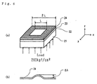
- Figure 6 (a) shows the polishing body that was used as the simulation model.
- a body having the shape of a rectangular solid was envisioned as the polishing body.
- SUBA22 an elastic nonwoven fabric
- SUS plate 23 stainless steel
- IC1000 24 a foam urethane
- the polishing surface had a square shape with dimensions of 2L on a side, and it was envisioned that this type of polishing body was pressed against the object of polishing with a commonly used pressure of 200 gf/cm 2 .
- the amount of recession of the IC1000 (amount of recession of the pad) ⁇ h shown in Figure 5 (b) was calculated with the thicknesses of the IC1000, SUS plate and SUBA varied. Furthermore, in a case where the "wafer global removal uniformity" was evaluated with the thickness of the Al fixed at 15 mm, L was set equal to 20 mm. This envisioned an extreme case in which the entire pattern of a typical chip constituted a recessed part. Furthermore, when the "local pattern planarity" was evaluated, L was set equal to 4 mm. The reason for this is that the envisioned maximum pattern interval was approximately 4 mm.
- Figure 7 shows one example of the results of a simulation of the "local pattern planarity."
- the horizontal axis in the figure shows the thickness of the IC1000, and the vertical axis shows the amount of recession of the IC1000 (amount of recession of the pad) ⁇ h .
- the curve indicated by a represents data for a case (single layer) in which the IC1000 was pasted directly to the Al base without installing an SUS plate or SUBA.
- the curve indicated by b represents data for a case (two layers) in which an SUBA was pasted to the Al base, and the IC1000 was pasted directly to the SUBA without installing an SUS plate.
- the curves indicated by c ( x ) represent data for cases (three layers) in which an SUBA was pasted to the Al base, an SUS plate with a thickness of x mm was pasted to the surface of the SUBA, and the IC1000 was pasted to the surface of the SUS plate. In cases where an SUBA was installed, the thickness was 1.27 mm in all instances.
- “Local pattern planarity” is considered to be improved as the amount of recession of the pad is smaller. In the case of a single layer, extremely good data are obtained. On the other hand, in the case of two layers, the amount of recession of the pad is large, and shows an abrupt increase especially in cases where the thickness of the IC1000 is small, which is undesirable. In the case of three layers, the amount of recession of the pad decreases as the thickness of the SUS plate is increased.
- the thickness of the SUS plate it is desirable to set the thickness of the SUS plate at 0.05 mm or greater, as a range in which data obtained when three layers are used are clearly superior to those obtained in the case of two layers. Furthermore, in cases where three layers are used, it is seen that the amount of recession of the pad becomes saturated when the thickness of the IC1000 exceeds 3 mm, so that it is desirable to set this thickness at 3 mm or less.
- Figure 8 shows one example of the results of a simulation of "wafer global removal uniformity.”
- the horizontal axis and vertical axis of the figure and the meanings of the curves in the figure are the same as in Figure 7.
- the thickness was 1.27 mm in all instances.
- the amount of recession of the pad be large; generally, an amount that is approximately five times the TTV is considered to be necessary. Accordingly, in cases where 1 ⁇ m is used as the currently accepted TTV, it is considered necessary that the amount of recession of the pad be 5 ⁇ m or greater.
- the thickness of the IC1000 is set at 3 mm or less as described above, this standard clearly cannot be satisfied in the case of a single layer, and even in cases where three layers are formed, this standard cannot be satisfied if the thickness of the IC1000 is small, unless the thickness of the SUS plate is 0.6 mm or less. Accordingly, it is desirable that the thickness of the SUS plate be set at 0.6 mm or less.
- the data shown in Figures 7 and 8 are data that were obtained in a case where the thickness of the SUBA was set at 1.27 mm as described above. In the simulation, the thickness of the SUBA was varied from 0.5 to 2.5 mm; however, the variation in the amount of recession of the pad caused by this variation in thickness was small. It is thought that the reason for this is as follows: specifically, since SUBA is a soft material, there is little effect on the amount of recession of the pad even if the thickness of the SUBA is varied.
- the polishing body and CMP polishing apparatus of the present invention can be used to polish wafers that have semiconductor circuit patterns in a semiconductor device manufacturing process. Furthermore, the semiconductor manufacturing method of the present invention can be used to manufacture semiconductor devices that have fine patterns.
Landscapes
- Engineering & Computer Science (AREA)
- Mechanical Engineering (AREA)
- Mechanical Treatment Of Semiconductor (AREA)
- Finish Polishing, Edge Sharpening, And Grinding By Specific Grinding Devices (AREA)
Abstract
The wafer 11 that is the object of polishing is held by a polishing head 12, and
rotates together with the polishing head 12. A polishing body 14 is attached to the
polishing member 13 by bonding using an adhesive agent or two-sided adhesive
tape, etc. As is shown in (b), the polishing body 14 is constructed by laminating a
soft member 15, a hard elastic member 16 and a polishing pad 17. The hard elastic
member 16 is constructed so that the amount of deformation of the hard elastic
member 16 at the polishing load that is applied during polishing is smaller than the
step difference that is permitted in the above-mentioned wafer in the interval
corresponding to the maximum pattern of the above-mentioned semiconductor
integrated circuits, and is larger than the TTV that is permitted in the above-mentioned
wafer in the interval corresponding to one chip. As a result, the
requirements of both "wafer global removal uniformity" and local pattern planarity"
can be satisfied.
Description
The present invention relates to a CMP polishing apparatus which is used to
polish wafers that have semiconductor integrated circuits formed inside, a polishing
body which is used in this CMP polishing apparatus, and a semiconductor device
manufacturing method which uses this CMP polishing apparatus.
As semiconductor integrated circuits have become finer and more highly
integrated, the individual processes involved in semiconductor manufacturing
processes have become more numerous and complicated. As a result, the surfaces of
semiconductor devices are not always flat. The presence of step differences on the
surfaces of semiconductor devices leads to step breakage of wiring and local
increases in resistance, etc., and thus causes wiring interruptions and drops in
electrical capacitance. In insulating films, furthermore, such step differences also
lead to a deterioration in the withstand voltage and the occurrence of leaks.
Meanwhile, as semiconductor integrated circuits have become finer and more
highly integrated, the wavelengths of light sources in semiconductor exposure
apparatuses used in photolithography have become shorter, and the numerical
aperture or so-called NA of the projection lenses used in such semiconductor
exposure apparatuses has become larger. As a result, the focal depth of the
projection lenses used in such semiconductor exposure apparatuses has become
substantially shallower. In order to deal with such increasing shallowness of the
focal depth, there is a demand for even greater planarization of the surfaces of
semiconductor devices than that achieved so far.
To describe this in concrete terms, planarization techniques such as that
shown in Figure 9 have become essential in semiconductor manufacturing processes.
Figure 9 is a schematic diagram illustrating planarization techniques used in a
semiconductor manufacturing process, and shows sectional views of a
semiconductor device. In Figure 9, 31 indicates a silicon wafer, 32 indicates an
inter-layer insulating film consisting of SiO2, 33 indicates a metal film consisting of
Cu, and 34 indicates the semiconductor device.
Figure 9 (a) shows an example of the planarization of an inter-layer
insulating film 32 on the surface of the semiconductor device. Figure 9 (b) shows an
example in which a so-called damascene is formed by polishing the metal film 33 on
the surface of the semiconductor device. A chemical mechanical polishing or
chemical mechanical planarization (hereafter referred to as "CMP") technique is
widely used as a method for planarizing the surfaces of such semiconductor devices.
Currently, the CMP technique is the sole method that can be used to planarize the
entire surface of a silicon wafer.
CMP was developed on the basis of silicon wafer mirror surface polishing
methods, and is performed using a CMP apparatus of the type shown in Figure 10.
In Figure 10, 35 indicates a polishing member, 36 indicates a member that holds
the object of polishing (hereafter referred to as a "polishing head" in some instances),
37 indicates a silicon wafer which is the object of polishing, 38 indicates a polishing
agent supply part, and 39 indicates a polishing agent. The polishing member 35
has a polishing pad 41 which is attached to the surface of a polishing platen 40. A
sheet-form foam polyurethane is widely used as such a polishing pad 41.
The object of polishing 37 is held by the polishing head 36, so that it is caused
to oscillate while being rotated, and is pressed against the polishing pad 41 of the
polishing member 35 with a specified pressure. The polishing member 35 is also
rotated, so that a relative motion is performed between the polishing member 35
and the object of polishing 37. In this state, the polishing agent 39 is supplied to
the surface of the polishing pad 41 from the polishing agent supply part 38. The
polishing agent 39 diffuses over the surface of the polishing pad 41, and enters the
space between the polishing pad 41 and the object of polishing 37 as the polishing
member 35 and object of polishing 37 move relative to each other, so that the
surface of the object of polishing 37 that is to be polished is polished. Specifically,
good polishing is accomplished by a synergistic effect of the mechanical polishing
caused by the relative motion of the polishing member 35 and object of polishing 37
and the chemical action of the polishing agent 39.
Unlike the surfaces of wafers in a blank state, the surfaces of wafers that
have semiconductor integrated circuits formed inside are not flat; in particular,
there are usually step differences between portions in which chips are formed and
portions in which chips are not formed. Accordingly, in cases where such wafers are
polished, there is a need to eliminate local indentations and projections (this is
called "local pattern planarity" while polishing the wafer in conformity to large
periodic indentations and projections (undulations) of the wafer substrate itself,
i.e., uniformly along such indentations and projections (undulations) (this is called
"wafer global removal uniformity").
In order to meet such demands, a method has been developed in which a
polishing body is formed by pasting together a polishing pad and a soft pad, and this
polishing body is used instead of the polishing pad 41 shown in Figure 10.
Specifically, as is shown in Figure 11, a polishing body 44 is formed by pasting
together a polishing pad 42 and a pad 43 which has a low elastic modulus and a
large compressive deformation rate, and this polishing body 44 is attached to the
polishing platen 40.
In such a state, when polishing of the type shown in Figure 10 is performed,
the pad 43 is caused to undergo compressive deformation by the force that is applied
to the large undulation of the wafer 37 via the polishing pad 42, so that the
polishing pad 42 also deforms in conformity to this deformation. Accordingly,
polishing can be performed in which the amount of polishing is fixed in accordance
with the undulation in the surface of the wafer 37. Meanwhile, in the case of local
indentations and projections, the deformation of the polishing pad 42 is relatively
small; accordingly, such indentations and projections can be removed by polishing.
In recent years, the degree of integration of semiconductor integrated circuits
has become increasingly higher; as a result, a wiring rule of 0.1 µm or less has
begun to be used. Furthermore, demand for the polishing of system LSIs has
increased, and in system LSIs, the distribution of pattern density has become
severe. In cases where wafers are polished which thus have patterns determined by
a fine wiring rule or patterns with a severe density distribution formed inside, it is
difficult to satisfy both the requirements of "wafer global removal uniformity" and
the requirements of "local pattern planarity" even if a polishing body of the above-mentioned
type is used. Specifically, in the case of such wafers, local indentations
and projections tend to be large; accordingly, as a result of the accompanying
compressive deformation of the pad 43 and the deformation of polishing pad 42 in
conformity to this deformation of the pad 43, it is difficult to ensure "local pattern
planarity."
The present invention was devised in order to solve such problems. The
object of the present invention is to provide a polishing body which can satisfy both
the requirements of "wafer global removal uniformity" and the requirements of
"local pattern planarity" even in cases where wafers are polished which have
patterns that use a wiring rule of 0.1 µm or less or patterns that have a severe
density distribution are formed inside, a CMP polishing apparatus using this
polishing body, and a semiconductor device manufacturing method using such a
CMP apparatus.
The first invention of the present application which is used to achieve the
above-mentioned object is a polishing body for a CMP polishing apparatus which is
used to polish wafers that have semiconductor integrated circuits formed inside,
wherein a polishing pad, a hard elastic member and a soft member are laminated in
that order, and the above-mentioned hard elastic member is constructed so that the
amount of deformation of this member at the polishing load that is applied during
polishing is smaller than the step difference permitted in the above-mentioned
wafer in an interval corresponding to the maximum pattern of the above-mentioned
semiconductor integrated circuits, and is greater than the TTV permitted in the
above-mentioned wafer in the interval corresponding to one chip.
Here, the term "TTV (total thickness variation)" refers to the indentations
and projections in the wafer as a whole. The interval corresponding to the
maximum pattern of the semiconductor integrated circuits and the interval
corresponding to one chip are shown in Figure 1.
Figure 1 (a) shows a sectional view of the wafer prior to polishing. In this
figure, 1 indicates the wafer substrate, 2 indicates patterns consisting of circuits
and wiring, etc., and 3 indicates an inter-layer insulating layer. The patterns 2
consisting of circuits and wiring are formed on the surface of the substrate 1, and
the inter-layer insulating layer 3 is formed on top of this, so that the patterns 2
consisting of circuits and wiring are insulated from each other. The interval
corresponding to the maximum pattern of the semiconductor integrated circuits
refers to the interval corresponding to the distance a of the recessed part of the
inter-layer insulating film 3 that covers the patterns 2 of circuits and wiring that
are most separated from each other within one chip. Currently, the interval
corresponding to the maximum pattern of such semiconductor integrated circuits is
approximately 4 mm.
Figure 1 (b) shows a single wafer, with a plurality of chips 5 being formed on
this wafer 1. The interval corresponding to one chip refers to the interval
corresponding to one side b in a case where the shape of the chip is square.
Currently, this interval is approximately 20 mm. In cases where the shape of the
chip is not square, or in cases where chips of different dimensions are formed on one
wafer, this interval refers to the distance corresponding to the largest side.
Furthermore, the hard elastic member refers to an elastic member with a
Young's modulus of 10,000 Kg/mm2 or greater; metal members may be cited as
typical examples. The soft member refers to a member that has a compression rate
of 10% or greater when a pressure of 1 Kg/cm2 is applied; chloroprene rubber
members containing air bubbles, or elastic nonwoven fabrics, may be cited as typical
examples.
In the present means, a hard elastic member is sandwiched between the
polishing pad and a soft member. Furthermore, the amount of deformation of this
hard elastic member at the load that is applied during polishing is set so that this
amount of deformation is smaller than the step difference that is permitted in the
above-mentioned wafer in the interval corresponding to the maximum pattern of
the above-mentioned semiconductor integrated circuits. Accordingly, since the hard
elastic member is not subjected to deformation exceeding the permitted step
difference in the interval corresponding to the maximum pattern, "local pattern
planarity" is ensured.
Meanwhile, the amount of deformation of the hard elastic member at the
polishing load that is applied during polishing is set so that this amount of
deformation is greater than the TTV permitted in the wafer in the interval
corresponding to one chip. Accordingly, the hard elastic member can deform in
conformity to the step difference over the distance corresponding to one chip, and
the polishing pad also shows a corresponding deformation in conformity to these
step differences, so that a uniform amount of polishing can be performed in
accordance with these step differences. Consequently, "wafer global removal
uniformity" is ensured.
The second invention of the present application that is used to achieve the
above-mentioned object is the polishing body of the first invention, wherein the
above-mentioned hard elastic member is constructed from a metal plate that will
not dissolve in the polishing agent.
In the above-mentioned first invention, there are no particular stipulations
regarding the material of the above-described hard elastic member. Accordingly, a
hard plastic or hard rubber, for example, can be used. However, a hard plastic or
hard rubber, etc., has a small Young's modulus; accordingly, if such a material is
used in the above-described first invention, the thickness of the member must be set
at a large value. If this thickness is increased, the degree of parallel orientation of
the two surfaces deteriorates; furthermore, irregularities in thermal expansion
occur as a result of temperature irregularities caused by the heat generated during
polishing, and such irregularities cause a deterioration in planarity.
In the present invention, since the above-described hard elastic member is
formed from a metal, the Young's modulus of the hard elastic member is high;
accordingly, the thickness of this member can be reduced. Consequently, the degree
of parallel orientation of the two surfaces can be maintained at a favorable value,
and irregularities in thermal expansion can be reduced, so that the planarity can be
maintained at a favorable value. Furthermore, the reason that the type of metal
used is limited to a metal that will not dissolve in the polishing agent is as follows:
specifically, if the metal dissolves in the polishing agent, there may be cases in
which this has a deleterious effect on the semiconductor integrated circuits that are
formed on the wafer. Stainless steel and titanium may be cited as examples of
metals that will not dissolve in commonly used polishing agents.
The third invention of the present application that is used to achieve the
above-mentioned object is the polishing body of the above-mentioned second
invention, wherein the above-mentioned metal plate is a stainless steel plate, and
the thickness h of this plate is such that 0.1 mm < h < 0.94 mm.
In the present means, in the case of a commonly polished wafer, the effect
described in the above-mentioned first means can be obtained; furthermore, the
effect described in the above-mentioned second means can also be obtained. In
addition, a stainless steel plate is readily available, and is less expensive than other
materials.
As will be described in the working configurations later, in cases where it is
assumed that the permitted step difference at a wiring rule of 0.35 µm is 0.35 µm
and that the TTV is 5 µm, it is assumed that the permitted step difference at a
wiring rule of 0.10 µm is 0.10 µm and that the TTV is 2 µm, and it is assumed that
the interval corresponding to the maximum pattern of the semiconductor integrated
circuits is 4 mm and that the interval corresponding to one chip is 20 mm, a
stainless steel thickness h which is such that 0.1 mm < h < 0.94 mm satisfies the
conditions fixed by the above-mentioned first invention at a surface pressure of
100 g/cm2 to 700 g/cm2. Accordingly, in the present invention, the thickness of the
stainless steel is limited as described above.
The fourth invention of the present application that is used to achieve the
above-mentioned object is a polishing body for a CMP polishing apparatus which is
used to polish wafers that have semiconductor integrated circuits formed inside,
wherein a polishing pad, a hard elastic member and a soft member are laminated in
that order, and these parts are constructed so that the combined amount of
deformation of the polishing pad, hard elastic member and soft member at the
polishing load that is applied during polishing is smaller than the height of the
indentations and projections of the above-mentioned maximum pattern in the
interval corresponding to the maximum pattern of the above-mentioned
semiconductor integrated circuits, and is greater than five times the TTV that is
permitted in the above-mentioned wafer.
The term "height of the indentations and projections of the maximum
pattern" refers to the depth of the recessed part corresponding to portion a in Figure
1 (a).
In the present means, a hard elastic member is sandwiched between the
polishing pad and a soft member. Furthermore, the combined amount of
deformation of the polishing pad, hard elastic member and soft member at the
polishing load that is applied during polishing is smaller than the height of the
indentations and projections of the above-mentioned maximum pattern in the
interval corresponding to the maximum pattern of the above-mentioned
semiconductor integrated circuits. Accordingly, since the polishing body is not
subjected to deformation exceeding the height of the indentations and projections of
the maximum pattern in the interval corresponding to the maximum pattern, the
step difference between patterns following polishing can be suppressed to a
difference that is less than the height of the indentations and projections of the
maximum pattern. Consequently, "local pattern planarity" is ensured.
Meanwhile, the combined amount of deformation of the polishing pad, hard
elastic member and soft member at the polishing load that is applied during
polishing is set so that this amount of deformation is greater than five times the
TTV that is permitted in the wafer in the interval corresponding to one chip.
Generally, it is known that the amount of deformation of the polishing body must be
five times the required TTV or greater if "wafer global removal uniformity" is to be
obtained. Accordingly, as a result of the combined amount of deformation of the
polishing pad, hard elastic member and soft member being set so that this amount
of deformation is greater than five times the TTV that is permitted in the wafer in
the interval corresponding to one chip, the polishing pad also deforms in conformity
to the step differences in cases where there are step differences in the distance
corresponding to one chip. Accordingly, a uniform amount of polishing can be
performed in accordance with these step differences. Consequently, "wafer global
removal uniformity" is ensured.
The fifth invention of the present application that is used to achieve the
above-mentioned object is the polishing body of the above-mentioned fourth
invention, wherein the above-mentioned hard elastic member is constructed from a
metal plate that will not dissolve in the polishing agent.
In the above-mentioned fourth invention, there are no particular stipulations
regarding the material of the above-mentioned hard elastic member. Accordingly, a
hard plastic or hard rubber, for example, can be used. However, since hard plastics
and hard rubbers, etc., have a small Young's modulus, the thickness must be
increased if such materials are used in the above-mentioned fourth means. When
the thickness increases, the degree of parallel orientation of the two surfaces
deteriorates; furthermore, irregularities in thermal expansion occur as a result of
temperature irregularities caused by the heat generated during polishing, and such
irregularities cause a deterioration in planarity.
In the present invention, since a metal is used as the material of the above-mentioned
hard elastic member, the Young's modulus is high; accordingly, the
thickness of the member can be reduced. Consequently, the degree of parallel
orientation of the two surfaces can be maintained at a favorable value, and
irregularities in thermal expansion can also be reduced, so that the planarity can be
maintained at a favorable value. Moreover, the reason that the type of metal used
is limited to a metal that will not dissolve in the polishing agent is as follows:
specifically, if the metal dissolves in the polishing agent, there are cases in which
this has a deleterious effect on the semiconductor integrated circuits that are
formed on the wafer. Examples of metals that will not dissolve in commonly used
polishing agents include stainless steel and titanium.
The sixth invention of the present application that is used to achieve the
above-mentioned object is the polishing body of the fifth invention, wherein the
above-mentioned polishing pad consists of a urethane foam material, the above-mentioned
metal plate is a stainless steel plate, the thickness of the above-mentioned
polishing pad is 0.1 to 3 mm, the thickness of the above-mentioned metal
body is 0.05 to 0.6 mm, and the thickness of the above-mentioned soft member is 0.5
to 2.5 mm.
A urethane foam material is superior as the material of a polishing pad;
furthermore, a stainless steel plate is easy to obtain, and is less expensive than
other materials. In cases where such materials are used, as will be described in the
embodiments later, the requirements of both "wafer global removal uniformity" and
"local pattern planarity" can be satisfied under advantageous conditions by setting
the thicknesses of the polishing pad, metal plate and soft member as described
above.
If the thickness of the polishing pad is less than 0.1 mm, the grooves used to
conduct the slurry, which are ordinarily formed in the polishing pad, are eliminated.
Accordingly, in the present means, the thickness of the polishing pad is limited to a
thickness of 0.1 mm or greater. Furthermore, even if the thickness of the polishing
pad exceeds 3 mm, no particular advantage is gained, and there is no great
difference between such a polishing body and a polishing body in which no metal
plate is sandwiched between the other parts as described above; accordingly, in the
present means, the thickness of the polishing pad is limited to a thickness of 3 mm
or less.
In cases where the thickness of the metal body is less than 0.05 mm, "local
pattern planarity" deteriorates as the thickness of the polishing pad is reduced, so
that there is no great difference between such a polishing body and a polishing body
in which no metal plate is sandwiched between the other parts as described above.
Accordingly, in the present means, the thickness of the metal body is limited to a
thickness of 0.05 mm or greater. On the other hand, if the thickness of the metal
body exceeds 0.6 mm, the limiting conditions of the above-mentioned fourth
invention cannot be realized in the case of a wafer with a TTV of 1 µm; accordingly,
in the present means, the thickness of the metal body is limited to a thickness of
0.6 mm or less.
Since the soft member is on the back surface of the metal body, the thickness
of the soft member does not greatly affect the "wafer global removal uniformity" or
"local pattern planarity." However, since an experiment (simulation) for the
purpose of deriving the limits on the above-mentioned respective numerical values
in the present invention was conducted in the range of 0.5 to 2.5 mm, the thickness
is limited to this range.
The seventh invention of the present application that is used to achieve the
above-mentioned object is the polishing body of any of the above-mentioned first
through sixth inventions, wherein the above-mentioned soft member has a torsional
strength which is such that this member is not damaged when the member rotates
with a load applied during polishing.
In the present invention, the above-mentioned soft member has a torsional
strength which is such that this member is not damaged when the member rotates
with a load applied during polishing; accordingly, polishing can be performed
smoothly.
The eighth invention of the present application that is used to achieve the
above-mentioned object is the polishing body of any of the above-mentioned first
through seventh inventions, wherein the above-mentioned hard elastic member and
soft member are fastened by bonding, and the above-mentioned hard elastic
member and polishing pad are fastened by vacuum suction.
In the present invention, since the hard elastic member and polishing pad are
fastened by vacuum suction, the polishing pad can easily be replaced when the
polishing pad becomes worn.
The ninth invention of the present application that is used to achieve the
above-mentioned object is the polishing body of any of the above-mentioned first
through seventh inventions, wherein the above-mentioned hard elastic member and
soft member are fastened by bonding means with a strong peeling strength, and the
above-mentioned hard elastic member and polishing pad are fastened by bonding
means with a weak peeling strength.
In the present invention, since the above-mentioned hard elastic member and
soft member are fastened by bonding means (adhesive agent or two-sided tape, etc.)
with a strong peeling strength, and the above-mentioned hard elastic member and
polishing pad are fastened by bonding means (adhesive agent or two-sided tape,
etc.) with a weak peeling strength, the polishing pad can be peeled from the hard
elastic member in a state in which the hard elastic member and soft member
remain bonded. Accordingly, the polishing pad can easily be replaced when the
polishing pad becomes worn.
The tenth invention of the present application that is used to achieve the
above-mentioned object is a CMP polishing apparatus which is used to polish wafers
that have semiconductor integrated circuits formed inside, and which has the
polishing body of any of the above-mentioned first through ninth inventions.
In the present invention, since the polishing body of one of the above-mentioned
first through ninth inventions is used, the effects described in the
descriptions of the respective polishing bodies can be obtained.
The eleventh invention of the present application that is used to achieve the
above-mentioned object is a CMP polishing apparatus which is used to polish wafers
that have semiconductor integrated circuits formed inside, and which has the
polishing body of the above-mentioned eighth or ninth invention, wherein the
dimensions of the above-mentioned polishing pad are set so that these dimensions
are smaller than the dimensions of the wafer that is being polished.
There are two types of CMP polishing apparatuses, i.e., apparatuses in which
the dimensions of the polishing pad are larger than the dimensions of the wafer
that is being polished, and apparatuses in which the dimensions of the polishing
pad are smaller than the dimensions of the wafer that is being polished. In the
present invention, the polishing body of the above-mentioned eighth or ninth
invention is used in the latter type of apparatus. Accordingly, since the size of the
polishing body pad is small, attachment by vacuum suction can easily be
accomplished, so that the polishing pad can be securely fastened to the hard elastic
member. Furthermore, in such a CMP apparatus, since the polishing pad is small,
frequent replacement of the polishing pad is necessary. Accordingly, an especially
great effect is obtained by using the polishing body of the above-mentioned eighth or
ninth invention, in which replacement of the polishing pad is easy.
The twelfth invention of the present application that is used to achieve the
above-mentioned object is a CMP polishing apparatus which is used to polish wafers
that have semiconductor integrated circuits formed inside, and which has the
polishing body of the above-mentioned seventh invention, wherein the dimensions
of the above-mentioned polishing pad are set so that these dimensions are smaller
than the dimensions of the wafer that is being polished, and the permissible shear
stress of the above-mentioned soft member is greater than 0.5 Kg/cm2.
According to findings obtained by the present inventors, in the case of a CMP
polishing apparatus in which the dimensions of the polishing pad are set so that
these dimensions are smaller than the dimensions of the wafer that is being
polished, the above-mentioned soft member can be endowed with a torsional
strength which is such the member is not damaged when the member rotates with a
load applied during polishing, by setting the permissible shear stress of the above-mentioned
soft member at a value that is greater than 0.5 Kg/cm2.
The thirteenth invention of the present application that is used to achieve the
above-mentioned object is a semiconductor device manufacturing method which is
characterized in that this method has a process in which the polishing of wafers is
performed using the CMP polishing apparatus of any of the abovementioned tenth
through twelfth inventions.
In the present invention, wafers can be polished while satisfying the
requirements of both "wafer global removal uniformity" and "local pattern
planarity," which are required in the polishing of wafers that have semiconductor
devices formed inside. Accordingly, a semiconductor exposure apparatus which has
a shallow focal depth can be used, and semiconductor devices that have fine
patterns can be manufactured with a good yield.
Below, examples of working configurations of the present invention will be
described with reference to the figures. However, these descriptions do not limit the
scope of the present invention.
Examples of working configurations of the present invention will be described
below with reference to the figures. Figure 2 (a) is a diagram which shows an
outline of a CMP polishing apparatus and a polishing body constituting one
example of a working configuration of the present invention. Figure 2 (b) is an
enlarged view of the portion labeled A in Figure 2 (a). In this working configuration,
the size of the polishing pad is smaller than the size of the wafer, unlike the case of
the conventional CMP apparatus shown in Figure 10.
The wafer 11 that is the object of polishing is held by a polishing head 12, and
rotates together with the polishing head 12. A polishing body 14 is attached to the
polishing member 13 by bonding using an adhesive agent or two-sided adhesive
tape, etc. As is shown in Figure 2 (b), the polishing body 14 is constructed by
laminating a soft member 15, a hard elastic member 16 and a polishing pad 17. In
this working configuration, the soft member 15, hard elastic member 16 and
polishing pad 17 are bonded by means of an adhesive agent or two-sided adhesive
tape, etc.
The polishing body 14 rotates together with the polishing member 13, and
swings at the same time; as a result, the polishing pad 17 polishes the entire
surface of the wafer 11. In this CMP apparatus as well, a polishing agent is
supplied to the area between the wafer 11 and the polishing pad 17; however, this is
not shown in the figures.
In the present working configuration, stainless steel is used as the material
of the hard elastic member 16. Furthermore, the thickness of the hard elastic
member 16 is determined so that the amount of deformation of the hard elastic
member 16 caused by the load during polishing is smaller than the step difference
that is permitted in the wafer in the interval corresponding to the maximum
pattern of the semiconductor integrated circuits, and is larger than the TTV that is
permitted in the wafer in the interval corresponding to one chip.
Assuming that the hard elastic member 16 is approximated as a rectangular
beam fastened at both ends, that the length of this beam is L, the thickness is h and
the Young's modulus is E, and that the surface pressure p is uniformly applied,
then the maximum amount of deformation w can be expressed as follows by
universally known calculations for a beam:
w = pL 4 / (32 Eh 3 )
In a case where the value of the interval corresponding to the maximum pattern is
4 mm, the value of the interval corresponding to one chip is 20 mm, and the device
wiring rule is 0.1 µm, then, assuming that the permitted step difference is 0.10 µm
and that the TTV is 2 µm, w in a case where L = 4 mm must be smaller than 0.1 µm,
and w in a case where L = 20 mm must be greater than 2 µm.
Assuming that the surface pressure p is 200 g/mm2, and that the Young's
modulus E of the stainless steel is 21,000 Kg/mm2, then the thickness h that
satisfies the above-mentioned conditions is a thickness which is such that
0.20 mm < h < 0.62 mm. If a hard plastic with a Young's modulus E of 400 Kg/mm2
is used instead of stainless steel, the thickness h is such that
0.74 mm < h < 2.32 mm. If the thickness is too great, there are many
inconveniences as described above; accordingly, it is desirable to use a metal which
allows a small thickness as the hard elastic member.
Table 1 shows the relationship between the surface pressure during polishing
and the limiting conditions on the thickness h in a cases where stainless steel is
used as the material of the hard elastic member 16. Here, the permitted step
difference in the case of a 0.35 µm wiring rule is set at 0.35 µm, and the TTV is set
at 5 µm.
| Material Stainless steel (E= 21,000 Kg/mm2) | Thickness h of hard sheet | |||
| 0.35 µm wiring rule (Permitted step difference = 0.35 µm; TTV = 5 µm) | 0.10 µm wiring rule (Permitted step difference = 0.10 µm; TTV = 2 µm) | |||
| L = 4 mm | L = 20 mm | L = 4 mm | L = 20 mm | |
| Surface pressure load | (w < 0.35 µm) | (w > 5 µm) | (w < 0.1 µm) | (w > 2 µm) |
| 100 g/cm2 | 0.10 mm | 0.36 mm | 0.16 mm | 0.49 mm |
| 200 g/cm2 | 0.13 mm | 0.46 mm | 0.20 mm | 0.62 mm |
| 300 g/cm2 | 0.15 mm | 0.52 mm | 0.23 mm | 0.71 mm |
| 400 g/cm2 | 0.16 mm | 0.58 mm | 0.25 mm | 0.78 mm |
| 500 g/cm2 | 0.18 mm | 0.62 mm | 0.27 mm | 0.84 mm |
| 600 g/cm2 | 0.19 mm | 0.66 mm | 0.28 mm | 0.89 mm |
| 700 g/cm2 | 0.20 mm | 0.69 mm | 0.30 mm | 0.94 mm |
It is desirable to use a member which has a large compressive deformation
and which tends not to undergo plastic deformation as the soft member 15. For
example, a chloroprene rubber, etc., which has air bubbles inside can be used as the
material of this member. However, it is desirable that this material have a
torsional strength which is such that the member is not damaged when the member
rotates with a load applied during polishing.
If this is done, the polishing pad 17 will conform to large undulations
corresponding to one chip, so that polishing in which the amount of polishing is
fixed can be performed, with the polishing pad 17 showing almost no deformation in
the case of local indentations and projections with a spacing corresponding to the
maximum spacing of the wiring pattern; accordingly, the requirements of both
"wafer global removal uniformity" and "local pattern planarity" can be satisfied.
Furthermore, as a separate approach in this working configuration, stainless
steel can be used as the material of the hard elastic member 16, and the thicknesses
of the respective members can be determined so that the combined deformation of
the polishing pad 17, hard elastic member 16 and soft member 15 caused by the
load during polishing is smaller than the height of the indentations and projections
of the maximum pattern in the interval corresponding to the maximum pattern of
the semiconductor integrated circuits, and greater than five times the TTV
permitted in the wafer in the interval corresponding to one chip in this working
configuration.
A member which shows a large compressive deformation and which tends not
to undergo plastic deformation is desirable as the soft member 15. For example, a
chloroprene rubber which has air bubbles inside, or an elastic nonwoven fabric, etc.
can be used. However, it is desirable to ensure that the material has a torsional
strength which is such that the member will not be damaged when the member
rotates with a load applied during polishing.
If this is done, the polishing pad 17 will conform to large undulations
corresponding to one chip, so that polishing in which the amount of polishing is
fixed can be performed, with the polishing body 14 showing almost no deformation
in the case of local indentations and projections with a spacing corresponding to the
maximum spacing of the wiring pattern; accordingly, the requirements of both
"wafer global removal uniformity" and "local pattern planarity" can be satisfied.
In Figure 2, in a case where the shape of the polishing pad is an annular
shape with an external diameter of D and an internal diameter of d, assuming that
the coefficient of friction between the wafer and polishing pad during polishing is k,
and that the surface pressure p is uniformly applied to the entire surface of the
polishing pad, the maximum torque T and maximum shear stress τmax applied to the
soft member 15 can be expressed as follows by universally known calculations:
T = kpπ (D 3 - d 3 ) / 12
τmax = 16DT /{π (D 4 - d 4 )}
= 4 kpD (D 3 - d 3 ) / {3(D 4 - d 4 )}
The graph in Figure 3 shows the results obtained when the relationship between
the surface pressure (polishing pressure) p (kg/cm2) and the maximum shear stress
τmax (kg/cm2) was determined by calculation in a cases where a polishing pad with
an external diameter D of 170 mm and an internal diameter d of 60 mm was used in
the CMP polishing apparatus shown in Figure 2, and the coefficient of friction k was
0.35. According to Figure 3, in a CMP polishing apparatus of the type shown in
Figure 2, the soft member 15 can be endowed with a torsional strength which is
such that the soft member 15 is not damaged under ordinary polishing conditions
(polishing pressure: 1.0 Kg/cm2) if the maximum shear stress τmax permitted in the
soft member 15 is greater than 0.5 Kg/cm2.
Figure 4 shows an outline (sectional view) of a polishing body constituting
another working configuration of the present invention. In Figure 4, constituent
elements that are the same as constituent elements shown in Figure 2 are labeled
with the same symbols, and a description of such elements is omitted. In the
working configuration shown in Figure 4 as well, the basic construction and the
materials of the soft member 15, hard elastic member 16 and polishing pad 17 are
the same as those shown in Figure 1.
In the working configuration shown in Figure 4, the soft member 15 is
bonded to the polishing member 13 by an adhesive agent or two-sided adhesive tape,
and the hard elastic member 16 is bonded to the soft member 15 by an adhesive
tape or two-sided adhesive tape. However, the hard elastic member 16 and the
polishing pad 17 are not bonded. Furthermore, holes 18 are formed which pass
through the polishing member 13, soft member 15 and hard elastic member 16, and
the polishing pad 17 is fastened to the hard elastic member 16 through vacuum
suction by setting the pressure inside these holes 18 at a low pressure that is close
to a vacuum in a state in which the polishing pad 17 is pressed against the hard
elastic member 16.
If this is done, then the polishing pad 17 can easily be removed merely by
releasing the vacuum state in cases where the polishing pad 17 is to be replaced as
a result of wear, so that replacement is easy. Especially in cases where a small-diameter
polishing pad whose dimensions are smaller than those of the wafer is
used, the number of holes 18 required is small, so that a vacuum suction
mechanism can easily be provided; accordingly, such a construction is effective.
Furthermore, in the case of a small-diameter pad, the frequency of replacement is
high; accordingly, the construction shown in Figure 4 is effective in this respect as
well.
Furthermore, even in cases where the soft member 15, hard elastic member
16 and polishing pad 17 are bonded only by bonding means such as an adhesive
agent or two-sided tape, the polishing pad 17 can easily be peeled from the hard
elastic member 16 by using bonding means with a strong peeling strength between
the polishing member 13 and soft member 15 and between the soft member 15 and
hard elastic member 16, and using bonding means with a weak peeling strength
between the hard elastic member 16 and polishing pad 17. As a result, the worn
polishing pad 17 can easily be replaced in the same manner as in the above-mentioned
working configuration in which a vacuum suction attachment
mechanism was provided.
Furthermore, it is desirable that the 180° peeling adhesive strength of the
adhesive layers between the polishing member 13 and soft member 15 and between
the soft member 15 and the hard elastic member 16 be greater than 1500 g/25 mm,
and that the 180° peeling adhesive strength of the adhesive layer between the hard
elastic member 16 and the polishing pad 17 be smaller than 1000 g/25 mm.
Figure 5 is a flow chart which shows a semiconductor device manufacturing
process constituting one example of a working configuration of the present
invention. After the semiconductor device manufacturing process is started, the
appropriate processing step is first selected in step S100 from the steps S101
through S104 described below. In accordance with this selection, the processing
proceeds to one of the steps S101 through S104.
Step S101 is an oxidation step in which the surface of the silicon wafer is
oxidized. Step S102 is a CVD step in which an insulating film is formed on the
surface of the silicon wafer by CVD, etc. Step S103 is an electrode formation step in
which electrodes are formed on the silicon wafer by a process such as vacuum
evaporation. Step S104 is an ion injection step in which ions are injected into the
silicon wafer.
Following the CVD step or electrode formation step, the processing proceeds
to step S105. In step S105, a judgement is made as to whether or not a CMP
process is to be performed, and in cases where such a process is to be performed, the
processing proceeds to the CMP process of step S106. In cases where a CMP
process is not to be performed, step S106 is bypassed. In the CMP process, the
flattening of inter-layer insulation films, or the formation of a damascene by the
polishing of metal films on the surfaces of semiconductor devices, etc., is performed
using the polishing apparatus of the present invention.
Following the CMP step or oxidation step, the processing proceeds to step
S107. Step S107 is a photolithographic step. In this photolithographic step, the
silicon wafer is coated with a resist, circuit patterns are burned onto the silicon
wafer by exposure using an exposure apparatus, and the exposed silicon wafer is
developed. Furthermore, the next step S108 is an etching step in which the
portions other than the developed resist image are removed by etching, the resist is
then peeled away, and the resist that has become unnecessary following etching is
removed.
Next, in step S109, a judgement is made as to whether or not all of the
necessary steps have been completed. If these steps have not been completed, the
processing returns to step S100, and the subsequent steps are repeated, so that
circuit patterns are formed on the silicon wafer. If it is judged in step S109 that all
of the steps have been completed, the process is ended.
Next, the results of a simulation based on the finite element method will be
described for examples of the polishing body of the present invention, and
comparative examples. Figure 6 (a) shows the polishing body that was used as the
simulation model. A body having the shape of a rectangular solid was envisioned as
the polishing body. As is shown in the figure, SUBA22 (an elastic nonwoven fabric)
was pasted to a base 21 consisting of Al, and an SUS plate 23 (stainless steel) was
laminated on top of this nonwoven fabric. Then, IC1000 24 (a foam urethane) was
pasted to the surface of this SUS plate 23. The IC1000 corresponds to the polishing
pad, the SUS corresponds to the hard elastic member, and the SUBA corresponds to
the soft member. The polishing surface had a square shape with dimensions of 2L
on a side, and it was envisioned that this type of polishing body was pressed against
the object of polishing with a commonly used pressure of 200 gf/cm2.
For the object of polishing, a hypothetical square hole with dimensions of L
on a side was assumed in the central portion of the polishing body. In order to
perform an equivalent simulation, a model was used in which the degree of freedom
of the surface-most portion of the IC1000 (which is hatched in Figure 6 (a)) was
constricted only in the z direction, and only the square portion with dimensions of L
on a side formed in the center was displaceable in the z direction as well (i.e., the
imaginary square shape with dimensions of L on a side could be recessed into the
hole).
Then, the amount of recession of the IC1000 (amount of recession of the pad)
Δh shown in Figure 5 (b) was calculated with the thicknesses of the IC1000, SUS
plate and SUBA varied. Furthermore, in a case where the "wafer global removal
uniformity" was evaluated with the thickness of the Al fixed at 15 mm, L was set
equal to 20 mm. This envisioned an extreme case in which the entire pattern of a
typical chip constituted a recessed part. Furthermore, when the "local pattern
planarity" was evaluated, L was set equal to 4 mm. The reason for this is that the
envisioned maximum pattern interval was approximately 4 mm.
Figure 7 shows one example of the results of a simulation of the "local
pattern planarity." The horizontal axis in the figure shows the thickness of the
IC1000, and the vertical axis shows the amount of recession of the IC1000 (amount
of recession of the pad) Δh. Among the curves shown in the figure, the curve
indicated by a represents data for a case (single layer) in which the IC1000 was
pasted directly to the Al base without installing an SUS plate or SUBA. The curve
indicated by b represents data for a case (two layers) in which an SUBA was pasted
to the Al base, and the IC1000 was pasted directly to the SUBA without installing
an SUS plate. The curves indicated by c(x) represent data for cases (three layers) in
which an SUBA was pasted to the Al base, an SUS plate with a thickness of x mm
was pasted to the surface of the SUBA, and the IC1000 was pasted to the surface of
the SUS plate. In cases where an SUBA was installed, the thickness was 1.27 mm
in all instances.
Furthermore, no difference was seen between c(0.94) and a in the effective
numerical range of the present calculations; accordingly, the curves of c(0.94) and a
coincide in the graph shown in Figure 7. Consequently, these coinciding curves are
indicated as a&c(0.94).
"Local pattern planarity" is considered to be improved as the amount of
recession of the pad is smaller. In the case of a single layer, extremely good data
are obtained. On the other hand, in the case of two layers, the amount of recession
of the pad is large, and shows an abrupt increase especially in cases where the
thickness of the IC1000 is small, which is undesirable. In the case of three layers,
the amount of recession of the pad decreases as the thickness of the SUS plate is
increased.
It is seen from this figure that it is desirable to set the thickness of the SUS
plate at 0.05 mm or greater, as a range in which data obtained when three layers
are used are clearly superior to those obtained in the case of two layers.
Furthermore, in cases where three layers are used, it is seen that the amount of
recession of the pad becomes saturated when the thickness of the IC1000 exceeds
3 mm, so that it is desirable to set this thickness at 3 mm or less.
Figure 8 shows one example of the results of a simulation of "wafer global
removal uniformity." The horizontal axis and vertical axis of the figure and the
meanings of the curves in the figure are the same as in Figure 7. Furthermore, in
cases where an SUBA was installed, the thickness was 1.27 mm in all instances.
In the case of "wafer global removal uniformity," it is considered desirable
that the amount of recession of the pad be large; generally, an amount that is
approximately five times the TTV is considered to be necessary. Accordingly, in
cases where 1 µm is used as the currently accepted TTV, it is considered necessary
that the amount of recession of the pad be 5 µm or greater.
Considering a case in which the thickness of the IC1000 is set at 3 mm or less
as described above, this standard clearly cannot be satisfied in the case of a single
layer, and even in cases where three layers are formed, this standard cannot be
satisfied if the thickness of the IC1000 is small, unless the thickness of the SUS
plate is 0.6 mm or less. Accordingly, it is desirable that the thickness of the SUS
plate be set at 0.6 mm or less.
The data shown in Figures 7 and 8 are data that were obtained in a case
where the thickness of the SUBA was set at 1.27 mm as described above. In the
simulation, the thickness of the SUBA was varied from 0.5 to 2.5 mm; however, the
variation in the amount of recession of the pad caused by this variation in thickness
was small. It is thought that the reason for this is as follows: specifically, since
SUBA is a soft material, there is little effect on the amount of recession of the pad
even if the thickness of the SUBA is varied.
The polishing body and CMP polishing apparatus of the present invention
can be used to polish wafers that have semiconductor circuit patterns in a
semiconductor device manufacturing process. Furthermore, the semiconductor
manufacturing method of the present invention can be used to manufacture
semiconductor devices that have fine patterns.
Claims (13)
- A polishing body for a CMP polishing apparatus which is used to polish wafers that have semiconductor integrated circuits formed inside, wherein a polishing pad, a hard elastic member and a soft member are laminated in that order, and the above-mentioned hard elastic member is constructed so that the amount of deformation of this member at the polishing load that is applied during polishing is smaller than the step difference permitted in the above-mentioned wafer in an interval corresponding to the maximum pattern of the above-mentioned semiconductor integrated circuits, and is greater than the TTV permitted in the above-mentioned wafer in the interval corresponding to one chip.
- The polishing body according to Claim 1, wherein the above-mentioned hard elastic member is constructed from a metal plate that will not dissolve in the polishing agent.
- The polishing body according to Claim 2, wherein the above-mentioned metal plate is a stainless steel plate, and the thickness h of this plate is such that 0.1 mm < h < 0.94 mm.
- A polishing body for a CMP polishing apparatus which is used to polish wafers that have semiconductor integrated circuits formed inside, wherein a polishing pad, a hard elastic member and a soft member are laminated in that order, and these parts are constructed so that the combined amount of deformation of the polishing pad, hard elastic member and soft member is smaller than the height of the indentations and projections of the above-mentioned maximum pattern in the interval corresponding to the maximum pattern of the above-mentioned semiconductor integrated circuits, and is greater than five times the TTV that is permitted in the above-mentioned wafer.
- The polishing body according to Claim 4, wherein the above-mentioned hard elastic member is constructed from a metal plate that will not dissolve in the polishing agent.
- The polishing body according to Claim 5, wherein the above-mentioned polishing pad consists of a urethane foam material, the above-mentioned metal plate is a stainless steel plate, the thickness of the above-mentioned polishing pad is 0.1 to 3 mm, the thickness of the above-mentioned metal body is 0.05 to 0.6 mm, and the thickness of the above-mentioned soft member is 0.5 to 2.5 mm.
- The polishing body according to any one of Claims 1 through 6, wherein the above-mentioned soft member has a torsional strength which is such that this member is not damaged when the member rotates with a load applied during polishing.
- The polishing body according to any one of Claims 1 through 7, wherein the above-mentioned hard elastic member and soft member are fastened by bonding, and the above-mentioned hard elastic member and polishing pad are fastened by vacuum suction.
- The polishing body according to any one of Claims 1 through 7, wherein the above-mentioned hard elastic member and soft member are fastened by bonding means with a strong peeling strength, and the above-mentioned hard elastic member and polishing pad are fastened by bonding means with a weak peeling strength.
- A CMP polishing apparatus which is used to polish wafers that have semiconductor integrated circuits formed inside, and which has the polishing body according to any one of Claims 1 through 9.
- A CMP polishing apparatus which is used to polish wafers that have semiconductor integrated circuits formed inside, and which has the polishing body according to Claim 8 or 9, wherein the dimensions of the above-mentioned polishing pad are set so that these dimensions are smaller than the dimensions of the wafer that is being polished.
- A CMP polishing apparatus which is used to polish wafers that have semiconductor integrated circuits formed inside, and which has the polishing body according to Claim 7, wherein the dimensions of the above-mentioned polishing pad are set so that these dimensions are smaller than the dimensions of the wafer that is being polished, and the permissible shear stress of the above-mentioned soft member is greater than 0.5 Kg/cm2.
- A semiconductor device manufacturing method which is characterized in that this method has a process in which the polishing of wafers is performed using the CMP polishing apparatus according to any one of Claims 10 through 12.
Applications Claiming Priority (3)
| Application Number | Priority Date | Filing Date | Title |
|---|---|---|---|
| JP2001219431 | 2001-07-19 | ||
| JP2001219431 | 2001-07-19 | ||
| PCT/JP2002/006780 WO2003009362A1 (en) | 2001-07-19 | 2002-07-04 | Polishing element, cmp polishing device and productionj method for semiconductor device |
Publications (2)
| Publication Number | Publication Date |
|---|---|
| EP1408538A1 true EP1408538A1 (en) | 2004-04-14 |
| EP1408538A4 EP1408538A4 (en) | 2008-07-09 |
Family
ID=19053436
Family Applications (1)
| Application Number | Title | Priority Date | Filing Date |
|---|---|---|---|
| EP02743826A Withdrawn EP1408538A4 (en) | 2001-07-19 | 2002-07-04 | POLISHING ELEMENT, MECHANICAL CHEMICAL POLISHING DEVICE (CMP) AND METHOD FOR PRODUCING SEMICONDUCTOR DEVICE |
Country Status (7)
| Country | Link |
|---|---|
| US (1) | US20040242132A1 (en) |
| EP (1) | EP1408538A4 (en) |
| JP (1) | JPWO2003009362A1 (en) |
| KR (1) | KR100564125B1 (en) |
| CN (1) | CN1224082C (en) |
| TW (1) | TW537945B (en) |
| WO (1) | WO2003009362A1 (en) |
Cited By (2)
| Publication number | Priority date | Publication date | Assignee | Title |
|---|---|---|---|---|
| US7189155B2 (en) | 2002-06-20 | 2007-03-13 | Nikon Corporation | Polishing body, polishing apparatus, semiconductor device, and semiconductor device manufacturing method |
| EP3479958A1 (en) * | 2017-11-07 | 2019-05-08 | Ebara Corporation | Substrate polishing device and polishing method |
Families Citing this family (16)
| Publication number | Priority date | Publication date | Assignee | Title |
|---|---|---|---|---|
| JP4876215B2 (en) * | 2005-01-21 | 2012-02-15 | 独立行政法人産業技術総合研究所 | CMP polishing method, CMP polishing apparatus, and semiconductor device manufacturing method |
| US7348276B2 (en) | 2005-03-30 | 2008-03-25 | Fujitsu, Limited | Fabrication process of semiconductor device and polishing method |
| JP4937538B2 (en) * | 2005-07-13 | 2012-05-23 | ニッタ・ハース株式会社 | Double-sided adhesive tape for fixing abrasive cloth and abrasive cloth provided with the same |
| KR101247065B1 (en) * | 2006-01-30 | 2013-03-25 | 엠이엠씨 일렉트로닉 머티리얼즈, 인크. | Double side wafer grinder and methods for assessing workpiece nanotopology |
| DE202006004193U1 (en) * | 2006-03-14 | 2006-06-08 | Richter, Harald | Adapter plate for a vacuum suction device |
| JP4998824B2 (en) * | 2007-06-12 | 2012-08-15 | 株式会社ニコン | Polishing pad size setting method |
| KR100901982B1 (en) * | 2007-07-12 | 2009-06-08 | 주식회사 실트론 | Adhesion Strength Tester |
| EP2242614A4 (en) * | 2007-12-31 | 2013-01-16 | Innopad Inc | CHIMICO-MECHANICAL PLANARIZATION BUFFER |
| DE102010040512B4 (en) | 2010-09-09 | 2016-03-10 | Infineon Technologies Ag | Chip with a high frequency switch assembly and circuitry, method for making a high frequency circuit arrangement |
| KR101596561B1 (en) * | 2014-01-02 | 2016-03-07 | 주식회사 엘지실트론 | Wafer polishing appratus |
| CN105500186A (en) * | 2016-01-21 | 2016-04-20 | 苏州新美光纳米科技有限公司 | Polishing pad for wafer polishing and self-absorption method thereof |
| JP6765267B2 (en) * | 2016-09-28 | 2020-10-07 | 株式会社ディスコ | Polishing unit |
| WO2020115867A1 (en) * | 2018-12-06 | 2020-06-11 | 三菱電機株式会社 | Osr attaching device and osr attaching method |
| CN109648463B (en) * | 2018-12-14 | 2021-04-23 | 厦门大学 | A kind of semiconductor wafer photoelectrochemical mechanical polishing processing method |
| CN113414717A (en) * | 2021-08-05 | 2021-09-21 | 燕山大学 | Composite cup-shaped polishing wheel and polishing method thereof |
| CN115704677B (en) * | 2021-08-13 | 2025-11-14 | 长鑫存储技术有限公司 | A metrological standard and its preparation method |
Family Cites Families (17)
| Publication number | Priority date | Publication date | Assignee | Title |
|---|---|---|---|---|
| US5287663A (en) * | 1992-01-21 | 1994-02-22 | National Semiconductor Corporation | Polishing pad and method for polishing semiconductor wafers |
| US5938504A (en) * | 1993-11-16 | 1999-08-17 | Applied Materials, Inc. | Substrate polishing apparatus |
| US5564965A (en) * | 1993-12-14 | 1996-10-15 | Shin-Etsu Handotai Co., Ltd. | Polishing member and wafer polishing apparatus |
| JP2891083B2 (en) * | 1993-12-14 | 1999-05-17 | 信越半導体株式会社 | Sheet-shaped polishing member and wafer polishing device |
| US6099954A (en) * | 1995-04-24 | 2000-08-08 | Rodel Holdings, Inc. | Polishing material and method of polishing a surface |
| JPH0950974A (en) * | 1995-08-07 | 1997-02-18 | Sony Corp | Polishing cloth and method for manufacturing semiconductor device |
| US5692950A (en) * | 1996-08-08 | 1997-12-02 | Minnesota Mining And Manufacturing Company | Abrasive construction for semiconductor wafer modification |
| JPH10156705A (en) * | 1996-11-29 | 1998-06-16 | Sumitomo Metal Ind Ltd | Polishing apparatus and polishing method |
| US5921856A (en) * | 1997-07-10 | 1999-07-13 | Sp3, Inc. | CVD diamond coated substrate for polishing pad conditioning head and method for making same |
| US5931724A (en) * | 1997-07-11 | 1999-08-03 | Applied Materials, Inc. | Mechanical fastener to hold a polishing pad on a platen in a chemical mechanical polishing system |
| US5882251A (en) * | 1997-08-19 | 1999-03-16 | Lsi Logic Corporation | Chemical mechanical polishing pad slurry distribution grooves |
| JP3152188B2 (en) * | 1997-11-28 | 2001-04-03 | 日本電気株式会社 | Polishing pad |
| JP2000077366A (en) * | 1998-08-28 | 2000-03-14 | Nitta Ind Corp | Polishing cloth and method of attaching and detaching the polishing cloth to and from a polishing machine surface plate |
| JP2001054859A (en) * | 1999-08-20 | 2001-02-27 | Nikon Corp | Polishing device and polishing member |
| JP2001160545A (en) * | 1999-12-02 | 2001-06-12 | Okamoto Machine Tool Works Ltd | Chemical mechanical polishing method of platinum layer on semiconductor substrate |
| US6402591B1 (en) * | 2000-03-31 | 2002-06-11 | Lam Research Corporation | Planarization system for chemical-mechanical polishing |
| US6561889B1 (en) * | 2000-12-27 | 2003-05-13 | Lam Research Corporation | Methods for making reinforced wafer polishing pads and apparatuses implementing the same |
-
2002
- 2002-07-04 JP JP2003514607A patent/JPWO2003009362A1/en active Pending
- 2002-07-04 US US10/467,627 patent/US20040242132A1/en not_active Abandoned
- 2002-07-04 WO PCT/JP2002/006780 patent/WO2003009362A1/en not_active Ceased
- 2002-07-04 KR KR1020037007085A patent/KR100564125B1/en not_active Expired - Lifetime
- 2002-07-04 CN CNB028059743A patent/CN1224082C/en not_active Expired - Lifetime
- 2002-07-04 EP EP02743826A patent/EP1408538A4/en not_active Withdrawn
- 2002-07-19 TW TW091116079A patent/TW537945B/en not_active IP Right Cessation
Cited By (3)
| Publication number | Priority date | Publication date | Assignee | Title |
|---|---|---|---|---|
| US7189155B2 (en) | 2002-06-20 | 2007-03-13 | Nikon Corporation | Polishing body, polishing apparatus, semiconductor device, and semiconductor device manufacturing method |
| EP3479958A1 (en) * | 2017-11-07 | 2019-05-08 | Ebara Corporation | Substrate polishing device and polishing method |
| US11331766B2 (en) | 2017-11-07 | 2022-05-17 | Ebara Corporation | Substrate polishing device and polishing method |
Also Published As
| Publication number | Publication date |
|---|---|
| CN1224082C (en) | 2005-10-19 |
| EP1408538A4 (en) | 2008-07-09 |
| KR20040010566A (en) | 2004-01-31 |
| CN1494734A (en) | 2004-05-05 |
| JPWO2003009362A1 (en) | 2004-11-11 |
| TW537945B (en) | 2003-06-21 |
| WO2003009362A1 (en) | 2003-01-30 |
| KR100564125B1 (en) | 2006-03-27 |
| US20040242132A1 (en) | 2004-12-02 |
Similar Documents
| Publication | Publication Date | Title |
|---|---|---|
| US20040242132A1 (en) | Polishing element, cmp polishing device and productionj method for semiconductor device | |
| US5287663A (en) | Polishing pad and method for polishing semiconductor wafers | |
| EP1295322B1 (en) | Two steps chemical mechanical polishing process | |
| US6435942B1 (en) | Chemical mechanical polishing processes and components | |
| US6580128B2 (en) | Semiconductor substrate, semiconductor device, and processes of production of same | |
| CN117476548A (en) | Chemical mechanical polishing for hybrid bonding | |
| US20060079159A1 (en) | Chemical mechanical polish with multi-zone abrasive-containing matrix | |
| JP3152188B2 (en) | Polishing pad | |
| KR100552435B1 (en) | Method of planarizing dielectric layer on semiconductor wafer | |
| WO1999046081A1 (en) | Multi-step chemical mechanical polishing process and device | |
| US6942549B2 (en) | Two-sided chemical mechanical polishing pad for semiconductor processing | |
| JP3115025B2 (en) | Polishing pad for semiconductor wafer and polishing method | |
| US20080064308A1 (en) | Polishing apparatus and manufacturing method of an electronic apparatus | |
| US7189155B2 (en) | Polishing body, polishing apparatus, semiconductor device, and semiconductor device manufacturing method | |
| JPH0950974A (en) | Polishing cloth and method for manufacturing semiconductor device | |
| US7108591B1 (en) | Compliant wafer chuck | |
| US6503811B1 (en) | Substrate having a semiconductor layer, and method for fabricating the same | |
| US20040259480A1 (en) | [polishing pad and process of chemical mechanical use thereof] | |
| US7252736B1 (en) | Compliant grinding wheel | |
| JP2003086549A (en) | Polishing tool, polishing apparatus, semiconductor device, and semiconductor device manufacturing method | |
| JP2001079755A (en) | Polishing body and polishing method | |
| US8403727B1 (en) | Pre-planarization system and method | |
| JP2003068843A (en) | Method for manufacturing semiconductor device | |
| JP2003007656A (en) | Method for manufacturing semiconductor device | |
| WO2004105113A1 (en) | Polishing body for cmp polishing, cmp polishing apparatus, cmp polishing method, and method for manufacturing semiconductor device |
Legal Events
| Date | Code | Title | Description |
|---|---|---|---|
| PUAI | Public reference made under article 153(3) epc to a published international application that has entered the european phase |
Free format text: ORIGINAL CODE: 0009012 |
|
| 17P | Request for examination filed |
Effective date: 20030728 |
|
| AK | Designated contracting states |
Kind code of ref document: A1 Designated state(s): AT BE CH CY DE DK ES FI FR GB GR IE IT LI LU MC NL PT SE TR |
|
| A4 | Supplementary search report drawn up and despatched |
Effective date: 20080609 |
|
| 17Q | First examination report despatched |
Effective date: 20080926 |
|
| STAA | Information on the status of an ep patent application or granted ep patent |
Free format text: STATUS: THE APPLICATION IS DEEMED TO BE WITHDRAWN |
|
| 18D | Application deemed to be withdrawn |
Effective date: 20090207 |