EP1408418A2 - Digital signal processor - Google Patents
Digital signal processor Download PDFInfo
- Publication number
- EP1408418A2 EP1408418A2 EP20030077876 EP03077876A EP1408418A2 EP 1408418 A2 EP1408418 A2 EP 1408418A2 EP 20030077876 EP20030077876 EP 20030077876 EP 03077876 A EP03077876 A EP 03077876A EP 1408418 A2 EP1408418 A2 EP 1408418A2
- Authority
- EP
- European Patent Office
- Prior art keywords
- event
- digital signal
- signal processor
- control unit
- accordance
- Prior art date
- Legal status (The legal status is an assumption and is not a legal conclusion. Google has not performed a legal analysis and makes no representation as to the accuracy of the status listed.)
- Withdrawn
Links
Images


Classifications
-
- G—PHYSICS
- G06—COMPUTING OR CALCULATING; COUNTING
- G06F—ELECTRIC DIGITAL DATA PROCESSING
- G06F15/00—Digital computers in general; Data processing equipment in general
- G06F15/76—Architectures of general purpose stored program computers
- G06F15/78—Architectures of general purpose stored program computers comprising a single central processing unit
- G06F15/7839—Architectures of general purpose stored program computers comprising a single central processing unit with memory
- G06F15/7842—Architectures of general purpose stored program computers comprising a single central processing unit with memory on one IC chip (single chip microcontrollers)
-
- G—PHYSICS
- G06—COMPUTING OR CALCULATING; COUNTING
- G06F—ELECTRIC DIGITAL DATA PROCESSING
- G06F9/00—Arrangements for program control, e.g. control units
- G06F9/06—Arrangements for program control, e.g. control units using stored programs, i.e. using an internal store of processing equipment to receive or retain programs
- G06F9/44—Arrangements for executing specific programs
- G06F9/448—Execution paradigms, e.g. implementations of programming paradigms
- G06F9/4494—Execution paradigms, e.g. implementations of programming paradigms data driven
Definitions
- the present invention relates to a digital signal processor that is driven by events.
- the processor comprises a central arithmetical unit, a register, a controller, an instruction memory, and input/output devices.
- control driven computing the basis is the predefined control procedure, stored as a program in machine code, describing in what sequence the information shall be processed.
- a data driven architecture the processing unit in the computer operates only if all input data is present in an input buffer and enough space is available in the output buffer to store the result.
- a demand driven architecture execution is initiated by demand of output data.
- event driven architecture event and time is introduced. Each unit start processing immediately when input data arrive, recognized as detection of an input event. Events are conventionally handled in the operative system. Event driven processing is primarily used in reconfigurable systems with lower performance. The lower performance is a trade-off to the possibility to alter the behavior in the system by means of programming.
- Compilers of today cannot map time or event expressed in software to lower level than the real-time operative system because time and event do not exist at the level below.
- the final execution of a single time or event expressed in the application software always ends up in the execution of a large number of machine code operations in sequence. This happens irrespective of computing architecture chosen for the application (control-, data-, demand- or event-driven). Consequently time performance for the final application is hard to guarantee because it is dependent of all simultaneous activities running on the processor and the real-time system.
- Achieved real-time performance is in general satisfying for mainstream applications, however it is too low real-time performance for more demanding applications. The consequence is that demanding applications cannot be implemented as a programmable application and executed on a digital signal processor.
- the event driven signal processor includes an arithmetic/logical unit , an internal register, a controller, an instruction memory and input/output devices as any conventional signal processor.
- the instruction memory is arranged to include time performance constraints and events.
- the controller in the event driven signal processor in accordance with claim 1 is arranged to suspend further processing of time performance constraints after initiating operations in an event control unit connected to the processor.
- the event control unit is arranged to recognize an event and to control the processing to be carried out as a consequence of the event. All processing is carried out under the time performance constraints.
- the controller resumes processing when advised by the event control unit.
- the invention also includes the specific embodiments disclosed in claims 2-10.
- two or more event control units are arranged in the processor. This allows the controller to proceed with processing of time performance constraints in one event control unit after initiating operations in another event control unit.
- the event driven signal processor in accordance with the invention provides for a reconfigurable event driven signal processor, which handle time constraints in an elegant way.
- the performance of the processor may easily be predicted deterministically without any uncertainty caused by cache misses or interfering real-time operative system.
- the event driven processor is particularly suitable for high-speed applications, e.g., radar applications, routers or network processing.
- Figure 1 discloses architecture for a first embodiment of an event driven processor 1 in accordance with the invention.
- the processor 1 is under control of a host processor, which is not disclosed in the figure. Input from the host processor is stored in the instruction memory 2.
- the processor 1 and the environment 8 form a real-time system.
- the instruction memory 2 holds operation code comprising logical operations as well as time constraints and events that will initiate operations within the processor 1.
- a controller 3 organizes reading and execution of the operation code in the instruction memory 2 so that everything is carried out in the correct sequence. Intermediate results are stored in a register 4 in conventional manner.
- An arithmetic and logical unit 5 is arranged to operate in a conventional manner.
- the processor 1 also includes an event control unit 6, which is capable of recognizing an event and to control the processing to be carried out as a consequence of the event while fulfilling the time performance constraints.
- the controller 3 initiates operations in the event control unit 6. After initiating operation, the controller 3 suspends further processing of time performance constraints and awaits an alert from the event control unit 6.
- the event control unit 6 controls the vector memory 7 and defines access to the vector memory 7 so that data is extracted or stored at the right moment in time. When advised by the event control unit 6 following detection of an event, the controller 3 resumes processing by initiating a new operation in the event control unit 6.
- the event-driven behavior is expressed in the instruction memory 2 as a chain or sequence of events with associated actions. An action is defined as an achievement expected as a direct consequence of the event. Events are executed in direct sequence where a succeeding action is processed directly after a previous action is completed. Each event control unit 6 start processing immediately when input data arrive, recognized as detection of an input event.
- the computed result is presented at the output at a time defined by a corresponding time constraint. Input and output buffering is not required.
- the controller 3 is responsible for defining, through the event control unit 6, which part of the vector memory 7 that should be used for certain data.
- the event control unit 6 regulates when data is extracted or stored.
- a vector memory 7 and an event control unit 6 allow events and time to be handled in the processor 1.
- time critical functionality can be moved from the level above real-time operating system to the event control unit 6.
- Figure 2 discloses an example of a typical event.
- the action is phase modulation illustrated by the square wave affecting the extracted data.
- event and time can be expressed as a pulse package operation with four operands: event, delay, vector and action .
- Event is an operand that defines the event that initiate execution.
- the delay operand defines a time constraint - a time interval to elapse between event and access to the vector memory 7 to extract or store data.
- Vector is an operand that defines location in the vector memory 7.
- the action operand defines future processing to be carried out on data after extraction or before storing in the vector memory 7.
- the event control unit 6 includes a package controller 9, which is a combined controller and time counter; an interface to the vector memory 7 and to external devices; and registers 10a, 10b to hold operands for pulse packages to facilitate momentary switch.
- An active register 10a holds the pulse package that is in process or to be processed at the next event.
- a buffer register 10b holds the subsequent pulse package to facilitate momentary switch between two subsequent pulse packages.
- Each register 10a, 10b is subdivided into four fields, each holding one operand.
- the event operand in the registers 10a, 10b selects which external or internal event signal that should initiate the execution.
- the delay field contains the time constraint.
- the delay operand is used to define a stop condition for the counter in the package controller 9.
- the vector operand is used by the package controller 9 to define the start and end position for signal data in the vector memory 7.
- the action field interfaces with external devices to control activity in these devices.
- a signal from the package controller 9 controls transfer of new operands from the buffer register 10b to the active register 10a.
- the package controller 9 will request new operands from the overlaying controller 3 using handshake signals. Execution of machine instructions in controller 3 is halted or resumed depending on the handshake signal.
- Figure 4 shows a second embodiment of the architecture for an event driven processor 1.
- the processor 1 is placed between Bus #1, connecting to host processor, and Bus #2, passing parameters to event control units 6a, 6b and to external devices such as a modulator 11 included in the output data path.
- the instruction memory 2 has two logically separated parts 2a, 2b to enable update of the operation codes in the instruction memory 2 under processing.
- the controller 3 manages the execution of operation codes for the event control units 6a, 6b as stored in the instruction memory parts 2a, 2b as separate jobs.
- the vector memory 7 can be a four-port SRAM, where two ports are used for connection to data paths to external devices with simultaneous read and write. The other two ports are connected to Bus #1 for parallel signal analysis.
- the controller 3 manages the execution of operation codes needed for the two event control units 6a, 6b, one for receiver function and one for transmitter function. Operation codes for the two functions are stored as separate jobs in the instruction memory 2.
- the event driven signal processor 1 is initialized by its host processor through Bus #1.
- the instruction memory 2 is loaded with code describing what actions to take when events arrive.
- the host processor starts an initial sequence of code to set up other hardware.
- the interconnection of the host processor and the event driven processor 1 by means of the instruction memory 2 enables a programmable behavior in the event driven processor 1.
- updating is carried out within a first part 2a of the instruction memory 2, which is not involved in the execution of operation code.
- the execution of operation code is carried out from this first part 2a. Updating of the second part 2b is then initiated. After programming, a first initiation sequence is executed.
- the event driven processor 1 suspends its processing and waits for an event to occur.
- the pulse package operation stored in the active register 10a is executed.
- the involved event control unit 6a/6b immediately initiates execution of the pulse package stored in the buffer register 10b.
- a request is sent to the controller 3 for new pulse packages.
- the request is accompanied by information of a job number, which is used by the controller 3 to resume execution of the corresponding job code in the instruction memory 2.
- each instruction tells the controller 3 if it should continue, wait and then continue or wait and then restart. More than one event can be handled in parallel. Actions taken upon events are reconfigurable by updating the code in the instruction code area.
- a first part 2a is being executed while the second part 2b is updated from Bus #1. It is possible to update behavior for one job or more by using the logical separation in a first and second part 2a, 2b in the instruction memory 2. For example, while the first part 2a is updated from host processor, the second part 2b is used for event actions. Further signal processing of data from the vector memory 7 is controlled via bus #2 to the modulator 11.
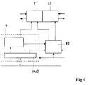
- High programmable time delay resolution is obtained by splitting the implementation of the delay field 10a2 in the active register 10a into two parts: a most significant part and a least significant part.
- the most significant part is passed to the package controller 9.
- a counter in the package controller 9 produces a delay as defined by the most significant part.
- data is extracted from the vector memory 7 and stored in an output buffer 13, which is part of the vector memory 7.
- the least significant part is passed to the high-speed controller 12 during the data extraction from the vector memory 7.
- a counter in the high-speed controller 12 produces a delay in a signal, which is passed from the package controller 9 to the high-speed controller 12 during data extraction from the vector memory 7.
- the high-speed controller 12 operates at the clock frequency and the counter in the package controller 9 operates at a lower frequency corresponding to the number of bits in the least significant part.
- Output data is stored in the buffer 13 until a signal: load_out_buffer, the delayed signal from the high-speed controller, becomes active. This signal is delayed as defined by the least significant part. Write is handled in a similar way.
- the event driven processor 1 in accordance with the invention allows large data packages transmitted with high speed, e.g., radar signals, to be received, processed and retransmitted with a timing control down to nanoseconds.
Landscapes
- Engineering & Computer Science (AREA)
- Theoretical Computer Science (AREA)
- Software Systems (AREA)
- Physics & Mathematics (AREA)
- General Engineering & Computer Science (AREA)
- General Physics & Mathematics (AREA)
- Computer Hardware Design (AREA)
- Complex Calculations (AREA)
- Power Sources (AREA)
- Advance Control (AREA)
Abstract
Description
- The present invention relates to a digital signal processor that is driven by events. The processor comprises a central arithmetical unit, a register, a controller, an instruction memory, and input/output devices.
- Depending on the architecture of a digital signal processor, the same type of functionality can be performed quite differently. In control driven computing the basis is the predefined control procedure, stored as a program in machine code, describing in what sequence the information shall be processed. In a data driven architecture the processing unit in the computer operates only if all input data is present in an input buffer and enough space is available in the output buffer to store the result. In a demand driven architecture, execution is initiated by demand of output data. In an event driven architecture event and time is introduced. Each unit start processing immediately when input data arrive, recognized as detection of an input event. Events are conventionally handled in the operative system. Event driven processing is primarily used in reconfigurable systems with lower performance. The lower performance is a trade-off to the possibility to alter the behavior in the system by means of programming.
- Compilers of today cannot map time or event expressed in software to lower level than the real-time operative system because time and event do not exist at the level below. The final execution of a single time or event expressed in the application software always ends up in the execution of a large number of machine code operations in sequence. This happens irrespective of computing architecture chosen for the application (control-, data-, demand- or event-driven). Consequently time performance for the final application is hard to guarantee because it is dependent of all simultaneous activities running on the processor and the real-time system. Achieved real-time performance is in general satisfying for mainstream applications, however it is too low real-time performance for more demanding applications. The consequence is that demanding applications cannot be implemented as a programmable application and executed on a digital signal processor.
- Various real-time operative systems have been developed for the purpose of handling time and parallel processes. These systems provide a possibility of expressing time by means of a real-time operative system call to a real-time clock. The real-time operative system also allows event to effect the program by means of routines for interrupt. Data-, demand-, and event-driven programmable behavioral is always possible to use to implement the application software on top of a platform consisting of a real-time operative system and a traditional control driven computing architecture. However, the event driven processing by means of the operative system cannot be performed with sufficient time resolution for many high-speed applications, e.g., radar. For these types of applications, event-driven processing is particularly favorable since the function of these type of applications many times depend upon when a specific action is performed. This can easily be expressed in an event-driven architecture.
- It is an object of the present invention to solve the problems in conventional event driven digital signal processors. This object is achieved through the digital signal processor in accordance with
claim 1. - The event driven signal processor includes an arithmetic/logical unit , an internal register, a controller, an instruction memory and input/output devices as any conventional signal processor. The instruction memory is arranged to include time performance constraints and events.
- The controller in the event driven signal processor in accordance with
claim 1 is arranged to suspend further processing of time performance constraints after initiating operations in an event control unit connected to the processor. The event control unit is arranged to recognize an event and to control the processing to be carried out as a consequence of the event. All processing is carried out under the time performance constraints. The controller resumes processing when advised by the event control unit. - The invention also includes the specific embodiments disclosed in claims 2-10. In a preferred embodiment, two or more event control units are arranged in the processor. This allows the controller to proceed with processing of time performance constraints in one event control unit after initiating operations in another event control unit.
- The event driven signal processor in accordance with the invention provides for a reconfigurable event driven signal processor, which handle time constraints in an elegant way. The performance of the processor may easily be predicted deterministically without any uncertainty caused by cache misses or interfering real-time operative system.
The event driven processor is particularly suitable for high-speed applications, e.g., radar applications, routers or network processing. -
- Fig. 1
- discloses an architecture in a control driven processor extended to an event driven processing architecture in accordance with the invention
- Fig. 2
- discloses the content of a one pulse package instruction
- Fig. 3
- discloses the internal structure of an event control unit
- Fig. 4
- discloses a block diagram of a second embodiment of an event driven processor
- Fig. 5
- discloses a structure to implement high-resolution time delay
- The preferred embodiments of the present invention will be described hereinafter with reference to the accompanying drawings.
- Figure 1 discloses architecture for a first embodiment of an event driven
processor 1 in accordance with the invention. Theprocessor 1 is under control of a host processor, which is not disclosed in the figure. Input from the host processor is stored in theinstruction memory 2. Theprocessor 1 and theenvironment 8 form a real-time system. Theinstruction memory 2 holds operation code comprising logical operations as well as time constraints and events that will initiate operations within theprocessor 1. Asignal memory 7, which can be a vector memory or any other suitable type of memory, stores signal data to be handled under the time-constraints in theprocessor 1. Acontroller 3 organizes reading and execution of the operation code in theinstruction memory 2 so that everything is carried out in the correct sequence. Intermediate results are stored in aregister 4 in conventional manner. An arithmetic andlogical unit 5 is arranged to operate in a conventional manner. Theprocessor 1 also includes anevent control unit 6, which is capable of recognizing an event and to control the processing to be carried out as a consequence of the event while fulfilling the time performance constraints. - The
controller 3 initiates operations in theevent control unit 6. After initiating operation, thecontroller 3 suspends further processing of time performance constraints and awaits an alert from theevent control unit 6. Theevent control unit 6 controls thevector memory 7 and defines access to thevector memory 7 so that data is extracted or stored at the right moment in time. When advised by theevent control unit 6 following detection of an event, thecontroller 3 resumes processing by initiating a new operation in theevent control unit 6. The event-driven behavior is expressed in theinstruction memory 2 as a chain or sequence of events with associated actions. An action is defined as an achievement expected as a direct consequence of the event. Events are executed in direct sequence where a succeeding action is processed directly after a previous action is completed. Eachevent control unit 6 start processing immediately when input data arrive, recognized as detection of an input event. The computed result is presented at the output at a time defined by a corresponding time constraint. Input and output buffering is not required. Thecontroller 3 is responsible for defining, through theevent control unit 6, which part of thevector memory 7 that should be used for certain data. Theevent control unit 6 regulates when data is extracted or stored. - With the event driven
processor 1 disclosed in fig 1, avector memory 7 and anevent control unit 6 allow events and time to be handled in theprocessor 1. With time constraints introduced in theprocessor 1, time critical functionality can be moved from the level above real-time operating system to theevent control unit 6. - Figure 2 discloses an example of a typical event. The action is phase modulation illustrated by the square wave affecting the extracted data. At machine instruction level event and time can be expressed as a pulse package operation with four operands: event, delay, vector and action.
Event is an operand that defines the event that initiate execution.
The delay operand defines a time constraint - a time interval to elapse between event and access to thevector memory 7 to extract or store data.
Vector is an operand that defines location in thevector memory 7.
The action operand defines future processing to be carried out on data after extraction or before storing in thevector memory 7. - An
event control unit 6 is disclosed in figure 3. Theevent control unit 6 includes apackage controller 9, which is a combined controller and time counter; an interface to thevector memory 7 and to external devices; andregisters active register 10a holds the pulse package that is in process or to be processed at the next event. Abuffer register 10b holds the subsequent pulse package to facilitate momentary switch between two subsequent pulse packages. Eachregister registers package controller 9. The vector operand is used by thepackage controller 9 to define the start and end position for signal data in thevector memory 7. The action field interfaces with external devices to control activity in these devices. A signal from thepackage controller 9 controls transfer of new operands from thebuffer register 10b to theactive register 10a. Immediately after completion of the transfer, thepackage controller 9 will request new operands from the overlayingcontroller 3 using handshake signals. Execution of machine instructions incontroller 3 is halted or resumed depending on the handshake signal. - Figure 4 shows a second embodiment of the architecture for an event driven
processor 1. Theprocessor 1 is placed betweenBus # 1, connecting to host processor, andBus # 2, passing parameters toevent control units modulator 11 included in the output data path. Theinstruction memory 2 has two logically separatedparts instruction memory 2 under processing. Thecontroller 3 manages the execution of operation codes for theevent control units instruction memory parts vector memory 7 can be a four-port SRAM, where two ports are used for connection to data paths to external devices with simultaneous read and write. The other two ports are connected toBus # 1 for parallel signal analysis. Thecontroller 3 manages the execution of operation codes needed for the twoevent control units instruction memory 2. - The event driven
signal processor 1 is initialized by its host processor throughBus # 1. Theinstruction memory 2 is loaded with code describing what actions to take when events arrive. The host processor starts an initial sequence of code to set up other hardware. The interconnection of the host processor and the event drivenprocessor 1 by means of theinstruction memory 2 enables a programmable behavior in the event drivenprocessor 1. During updating of theinstruction memory 2, updating is carried out within afirst part 2a of theinstruction memory 2, which is not involved in the execution of operation code. When the update has been terminated for thefirst part 2a, the execution of operation code is carried out from thisfirst part 2a. Updating of thesecond part 2b is then initiated. After programming, a first initiation sequence is executed. After initiation, the event drivenprocessor 1 suspends its processing and waits for an event to occur. When an event is detected, the pulse package operation stored in theactive register 10a is executed. After execution of the pulse package is completed, the involvedevent control unit 6a/6b immediately initiates execution of the pulse package stored in thebuffer register 10b. A request is sent to thecontroller 3 for new pulse packages. The request is accompanied by information of a job number, which is used by thecontroller 3 to resume execution of the corresponding job code in theinstruction memory 2. When a job is processed, each instruction tells thecontroller 3 if it should continue, wait and then continue or wait and then restart. More than one event can be handled in parallel. Actions taken upon events are reconfigurable by updating the code in the instruction code area. Afirst part 2a is being executed while thesecond part 2b is updated fromBus # 1. It is possible to update behavior for one job or more by using the logical separation in a first andsecond part instruction memory 2. For example, while thefirst part 2a is updated from host processor, thesecond part 2b is used for event actions. Further signal processing of data from thevector memory 7 is controlled viabus # 2 to themodulator 11. - High programmable time delay resolution is obtained by splitting the implementation of the delay field 10a2 in the
active register 10a into two parts: a most significant part and a least significant part. The most significant part is passed to thepackage controller 9. A counter in thepackage controller 9 produces a delay as defined by the most significant part. Following the delay, data is extracted from thevector memory 7 and stored in anoutput buffer 13, which is part of thevector memory 7. The least significant part is passed to the high-speed controller 12 during the data extraction from thevector memory 7. A counter in the high-speed controller 12 produces a delay in a signal, which is passed from thepackage controller 9 to the high-speed controller 12 during data extraction from thevector memory 7. The high-speed controller 12 operates at the clock frequency and the counter in thepackage controller 9 operates at a lower frequency corresponding to the number of bits in the least significant part. Output data is stored in thebuffer 13 until a signal: load_out_buffer, the delayed signal from the high-speed controller, becomes active. This signal is delayed as defined by the least significant part. Write is handled in a similar way. - The event driven
processor 1 in accordance with the invention allows large data packages transmitted with high speed, e.g., radar signals, to be received, processed and retransmitted with a timing control down to nanoseconds.
Claims (10)
- A digital signal processor (1) comprising:characterized in thatan instruction memory (2), a central arithmetic unit 5, a register (4), a controller (3),and input/output devices;the instruction memory (2) is arranged to include time performance constraints and event;the controller (3) is arranged to suspend further processing of time performance constraints after initiating operations in an event control unit (6);the event control unit(6) is arranged to recognize an event and to control processing to be carried out as a consequence of the event while fulfilling the time performance constraints andthe controller (3) is arranged to resume processing when advised by the event control unit (6).
- A digital signal processor (1) in accordance with claim 1, wherein the event is recognized in a detector and introduced as a level transition to the event control unit (6).
- A digital signal processor (1) in accordance with claim 2, wherein the detector is arranged to detect input signals by determining the energy level in the signal.
- A digital signal processor (1) in accordance with claim 2 or 3, wherein a further event is recognized as a completion of the processing carried out as a consequence of the previous event.
- A digital signal processor (1) in accordance with claim 1, wherein the event is recognized as a completion of the processing carried out as a consequence of the previous event.
- A digital signal processor (1) in accordance with claim 1, including a signal memory (7) arranged to store and extract data under control of the event control unit (6).
- A digital signal processor (1) in accordance with claim 6, wherein the signal memory (7) is a vector memory with low granularity and where the granularity determines a split between a high-resolution part and a low-resolution part of the time performance constraints.
- A digital signal processor (1) in accordance with claim 7, wherein the event control unit (6) is arranged to process the low-resolution part.
- A digital signal processor (1) in accordance with claim 7, wherein the high-resolution part is processed during memory access to the signal memory (7) by delaying the access to the signal memory (7) a period of time corresponding to the high-resolution part..
- A digital signal processor 1 in accordance with claim 1, including two or more event control units (6a, 6b) arranged to work independently from each other.
Applications Claiming Priority (2)
| Application Number | Priority Date | Filing Date | Title |
|---|---|---|---|
| SE0202792A SE524606C2 (en) | 2002-09-20 | 2002-09-20 | A digital signal processor that is event controlled |
| SE0202792 | 2002-09-20 |
Publications (2)
| Publication Number | Publication Date |
|---|---|
| EP1408418A2 true EP1408418A2 (en) | 2004-04-14 |
| EP1408418A3 EP1408418A3 (en) | 2007-01-31 |
Family
ID=20289051
Family Applications (1)
| Application Number | Title | Priority Date | Filing Date |
|---|---|---|---|
| EP03077876A Withdrawn EP1408418A3 (en) | 2002-09-20 | 2003-09-12 | Digital signal processor |
Country Status (3)
| Country | Link |
|---|---|
| US (1) | US7818549B2 (en) |
| EP (1) | EP1408418A3 (en) |
| SE (1) | SE524606C2 (en) |
Families Citing this family (3)
| Publication number | Priority date | Publication date | Assignee | Title |
|---|---|---|---|---|
| JP4994254B2 (en) * | 2007-03-08 | 2012-08-08 | ルネサスエレクトロニクス株式会社 | Data processor and control system |
| US10198062B2 (en) * | 2009-11-20 | 2019-02-05 | Nxp B.V. | Microprocessor to resume clocking and execution based on external input pattern detection |
| WO2012118917A2 (en) | 2011-03-03 | 2012-09-07 | Social Communications Company | Realtime communications and network browsing client |
Family Cites Families (11)
| Publication number | Priority date | Publication date | Assignee | Title |
|---|---|---|---|---|
| US4497023A (en) * | 1982-11-04 | 1985-01-29 | Lucasfilm Ltd. | Linked list of timed and untimed commands |
| US5021945A (en) * | 1985-10-31 | 1991-06-04 | Mcc Development, Ltd. | Parallel processor system for processing natural concurrencies and method therefor |
| US5220676A (en) * | 1991-04-19 | 1993-06-15 | Motorola, Inc. | Synchronization method and apparatus |
| US5768602A (en) * | 1995-08-04 | 1998-06-16 | Apple Computer, Inc. | Sleep mode controller for power management |
| US5826072A (en) * | 1995-11-13 | 1998-10-20 | Oasis Design, Inc. | Pipelined digital signal processor and signal processing system employing same |
| US5913058A (en) * | 1997-09-30 | 1999-06-15 | Compaq Computer Corp. | System and method for using a real mode bios interface to read physical disk sectors after the operating system has loaded and before the operating system device drivers have loaded |
| US6567839B1 (en) * | 1997-10-23 | 2003-05-20 | International Business Machines Corporation | Thread switch control in a multithreaded processor system |
| US6308197B1 (en) * | 1998-04-29 | 2001-10-23 | Xerox Corporation | Machine control using register construct |
| US6292887B1 (en) * | 1999-03-31 | 2001-09-18 | International Business Machines Corp. | System and method for synchronizing instruction execution with external events |
| US6892167B2 (en) * | 2001-11-28 | 2005-05-10 | Sypris Data Systems, Inc. | Real-time data acquisition and storage network |
| US20040088704A1 (en) * | 2002-10-30 | 2004-05-06 | Advanced Simulation Technology, Inc. | Method for running real-time tasks alongside a general purpose operating system |
-
2002
- 2002-09-20 SE SE0202792A patent/SE524606C2/en not_active IP Right Cessation
-
2003
- 2003-09-12 EP EP03077876A patent/EP1408418A3/en not_active Withdrawn
- 2003-09-22 US US10/665,290 patent/US7818549B2/en not_active Expired - Fee Related
Non-Patent Citations (1)
| Title |
|---|
| CONFERENCE, vol. 2438, 2 September 2002 (2002-09-02), pages 945 - 954 |
Also Published As
| Publication number | Publication date |
|---|---|
| SE0202792L (en) | 2004-03-21 |
| US20040128491A1 (en) | 2004-07-01 |
| SE0202792D0 (en) | 2002-09-20 |
| SE524606C2 (en) | 2004-08-31 |
| US7818549B2 (en) | 2010-10-19 |
| EP1408418A3 (en) | 2007-01-31 |
Similar Documents
| Publication | Publication Date | Title |
|---|---|---|
| KR100570138B1 (en) | System and method for loading software on a plurality of processors | |
| WO1990014629A2 (en) | Parallel multithreaded data processing system | |
| EP0272705B1 (en) | Loosely coupled pipeline processor | |
| EP1990718A1 (en) | Method and apparatus for loading data and instructions into a computer | |
| US4773041A (en) | System for executing a sequence of operation codes with some codes being executed out of order in a pipeline parallel processor | |
| JPH0778088A (en) | Apparatus for processing of plurality of interrupts in processor system and method for responding to interrupt from plurality of interrupt triggers in processor system as well as method and apparatus for simultaneous task between plurality of processors | |
| JP2884831B2 (en) | Processing equipment | |
| EP0290942B1 (en) | Guest machine execution control system for virtual machine system | |
| US7818549B2 (en) | Event driven digital signal processor with time constraints | |
| US20160246740A1 (en) | Processor system having nested vectored interrupt controller | |
| EP1821202B1 (en) | Execution of instructions directly from input source | |
| US7107478B2 (en) | Data processing system having a Cartesian Controller | |
| JP2591200B2 (en) | Program prefetching device | |
| JPH06324861A (en) | System and method for controlling cpu | |
| Bellini et al. | Exploiting a Real-Time Linux platform in controlling robotic manipulators | |
| JPH04268928A (en) | Emulation device and semiconductor device | |
| WO1993018451A1 (en) | Elimination of the critical path in memory control unit and input/output control unit operations | |
| JP2872042B2 (en) | Shared memory access method | |
| JP2583614B2 (en) | Vector arithmetic unit | |
| JPH0243626A (en) | Apparatus for controlling execution speed of computer processor | |
| JPH03257634A (en) | Method and device for parallelly processing program | |
| JPH07334215A (en) | Programmable controller sequence control method | |
| JPH04362741A (en) | Interruption control method | |
| JPH06100962B2 (en) | Bus control circuit | |
| JPH0766325B2 (en) | Pipeline control equipment |
Legal Events
| Date | Code | Title | Description |
|---|---|---|---|
| PUAI | Public reference made under article 153(3) epc to a published international application that has entered the european phase |
Free format text: ORIGINAL CODE: 0009012 |
|
| AK | Designated contracting states |
Kind code of ref document: A2 Designated state(s): AT BE BG CH CY CZ DE DK EE ES FI FR GB GR HU IE IT LI LU MC NL PT RO SE SI SK TR |
|
| AX | Request for extension of the european patent |
Extension state: AL LT LV MK |
|
| PUAL | Search report despatched |
Free format text: ORIGINAL CODE: 0009013 |
|
| AK | Designated contracting states |
Kind code of ref document: A3 Designated state(s): AT BE BG CH CY CZ DE DK EE ES FI FR GB GR HU IE IT LI LU MC NL PT RO SE SI SK TR |
|
| AX | Request for extension of the european patent |
Extension state: AL LT LV MK |
|
| 17P | Request for examination filed |
Effective date: 20070522 |
|
| AKX | Designation fees paid |
Designated state(s): AT BE BG CH CY CZ DE DK EE ES FI FR GB GR HU IE IT LI LU MC NL PT RO SE SI SK TR |
|
| 17Q | First examination report despatched |
Effective date: 20080118 |
|
| STAA | Information on the status of an ep patent application or granted ep patent |
Free format text: STATUS: THE APPLICATION IS DEEMED TO BE WITHDRAWN |
|
| 18D | Application deemed to be withdrawn |
Effective date: 20130403 |