EP1407315B1 - Electro-absorption modulated laser with high operating temperature tolerance - Google Patents
Electro-absorption modulated laser with high operating temperature tolerance Download PDFInfo
- Publication number
- EP1407315B1 EP1407315B1 EP02744691.3A EP02744691A EP1407315B1 EP 1407315 B1 EP1407315 B1 EP 1407315B1 EP 02744691 A EP02744691 A EP 02744691A EP 1407315 B1 EP1407315 B1 EP 1407315B1
- Authority
- EP
- European Patent Office
- Prior art keywords
- semiconductor layer
- electro
- absorption
- laser
- modulator
- Prior art date
- Legal status (The legal status is an assumption and is not a legal conclusion. Google has not performed a legal analysis and makes no representation as to the accuracy of the status listed.)
- Expired - Lifetime
Links
- 238000010521 absorption reaction Methods 0.000 title claims description 101
- 239000004065 semiconductor Substances 0.000 claims description 156
- 239000000463 material Substances 0.000 claims description 44
- 230000003287 optical effect Effects 0.000 claims description 43
- 230000005540 biological transmission Effects 0.000 claims description 23
- 230000004044 response Effects 0.000 claims description 22
- 230000001902 propagating effect Effects 0.000 claims description 20
- 239000000203 mixture Substances 0.000 claims description 18
- 238000000034 method Methods 0.000 claims description 12
- 239000000758 substrate Substances 0.000 claims description 10
- 230000008859 change Effects 0.000 claims description 8
- 230000003028 elevating effect Effects 0.000 claims description 2
- GPXJNWSHGFTCBW-UHFFFAOYSA-N Indium phosphide Chemical compound [In]#P GPXJNWSHGFTCBW-UHFFFAOYSA-N 0.000 description 9
- 238000010586 diagram Methods 0.000 description 8
- 238000002955 isolation Methods 0.000 description 7
- 230000008901 benefit Effects 0.000 description 5
- 238000001816 cooling Methods 0.000 description 5
- 230000005684 electric field Effects 0.000 description 5
- 238000005530 etching Methods 0.000 description 5
- 230000008033 biological extinction Effects 0.000 description 4
- 239000013307 optical fiber Substances 0.000 description 4
- 230000035945 sensitivity Effects 0.000 description 3
- 239000006163 transport media Substances 0.000 description 3
- 238000005253 cladding Methods 0.000 description 2
- 238000000295 emission spectrum Methods 0.000 description 2
- 230000009467 reduction Effects 0.000 description 2
- 229910000530 Gallium indium arsenide Inorganic materials 0.000 description 1
- 230000004888 barrier function Effects 0.000 description 1
- 239000003990 capacitor Substances 0.000 description 1
- 238000005229 chemical vapour deposition Methods 0.000 description 1
- 150000001875 compounds Chemical class 0.000 description 1
- 239000013078 crystal Substances 0.000 description 1
- 230000007423 decrease Effects 0.000 description 1
- 239000006185 dispersion Substances 0.000 description 1
- 230000000694 effects Effects 0.000 description 1
- 230000008030 elimination Effects 0.000 description 1
- 238000003379 elimination reaction Methods 0.000 description 1
- 239000000835 fiber Substances 0.000 description 1
- 230000005669 field effect Effects 0.000 description 1
- 230000002706 hydrostatic effect Effects 0.000 description 1
- 230000031700 light absorption Effects 0.000 description 1
- 238000012538 light obscuration Methods 0.000 description 1
- 229910052751 metal Inorganic materials 0.000 description 1
- 239000002184 metal Substances 0.000 description 1
- 230000000644 propagated effect Effects 0.000 description 1
- 230000006798 recombination Effects 0.000 description 1
- 238000005215 recombination Methods 0.000 description 1
- 230000003595 spectral effect Effects 0.000 description 1
- 230000001360 synchronised effect Effects 0.000 description 1
- 238000001947 vapour-phase growth Methods 0.000 description 1
Images




Classifications
-
- H—ELECTRICITY
- H01—ELECTRIC ELEMENTS
- H01S—DEVICES USING THE PROCESS OF LIGHT AMPLIFICATION BY STIMULATED EMISSION OF RADIATION [LASER] TO AMPLIFY OR GENERATE LIGHT; DEVICES USING STIMULATED EMISSION OF ELECTROMAGNETIC RADIATION IN WAVE RANGES OTHER THAN OPTICAL
- H01S5/00—Semiconductor lasers
- H01S5/02—Structural details or components not essential to laser action
- H01S5/026—Monolithically integrated components, e.g. waveguides, monitoring photo-detectors, drivers
- H01S5/0265—Intensity modulators
-
- B—PERFORMING OPERATIONS; TRANSPORTING
- B82—NANOTECHNOLOGY
- B82Y—SPECIFIC USES OR APPLICATIONS OF NANOSTRUCTURES; MEASUREMENT OR ANALYSIS OF NANOSTRUCTURES; MANUFACTURE OR TREATMENT OF NANOSTRUCTURES
- B82Y20/00—Nanooptics, e.g. quantum optics or photonic crystals
-
- G—PHYSICS
- G02—OPTICS
- G02F—OPTICAL DEVICES OR ARRANGEMENTS FOR THE CONTROL OF LIGHT BY MODIFICATION OF THE OPTICAL PROPERTIES OF THE MEDIA OF THE ELEMENTS INVOLVED THEREIN; NON-LINEAR OPTICS; FREQUENCY-CHANGING OF LIGHT; OPTICAL LOGIC ELEMENTS; OPTICAL ANALOGUE/DIGITAL CONVERTERS
- G02F1/00—Devices or arrangements for the control of the intensity, colour, phase, polarisation or direction of light arriving from an independent light source, e.g. switching, gating or modulating; Non-linear optics
- G02F1/01—Devices or arrangements for the control of the intensity, colour, phase, polarisation or direction of light arriving from an independent light source, e.g. switching, gating or modulating; Non-linear optics for the control of the intensity, phase, polarisation or colour
- G02F1/015—Devices or arrangements for the control of the intensity, colour, phase, polarisation or direction of light arriving from an independent light source, e.g. switching, gating or modulating; Non-linear optics for the control of the intensity, phase, polarisation or colour based on semiconductor elements having potential barriers, e.g. having a PN or PIN junction
- G02F1/017—Structures with periodic or quasi periodic potential variation, e.g. superlattices, quantum wells
- G02F1/01708—Structures with periodic or quasi periodic potential variation, e.g. superlattices, quantum wells in an optical wavequide structure
-
- G—PHYSICS
- G02—OPTICS
- G02F—OPTICAL DEVICES OR ARRANGEMENTS FOR THE CONTROL OF LIGHT BY MODIFICATION OF THE OPTICAL PROPERTIES OF THE MEDIA OF THE ELEMENTS INVOLVED THEREIN; NON-LINEAR OPTICS; FREQUENCY-CHANGING OF LIGHT; OPTICAL LOGIC ELEMENTS; OPTICAL ANALOGUE/DIGITAL CONVERTERS
- G02F1/00—Devices or arrangements for the control of the intensity, colour, phase, polarisation or direction of light arriving from an independent light source, e.g. switching, gating or modulating; Non-linear optics
- G02F1/01—Devices or arrangements for the control of the intensity, colour, phase, polarisation or direction of light arriving from an independent light source, e.g. switching, gating or modulating; Non-linear optics for the control of the intensity, phase, polarisation or colour
- G02F1/0121—Operation of devices; Circuit arrangements, not otherwise provided for in this subclass
-
- G—PHYSICS
- G02—OPTICS
- G02F—OPTICAL DEVICES OR ARRANGEMENTS FOR THE CONTROL OF LIGHT BY MODIFICATION OF THE OPTICAL PROPERTIES OF THE MEDIA OF THE ELEMENTS INVOLVED THEREIN; NON-LINEAR OPTICS; FREQUENCY-CHANGING OF LIGHT; OPTICAL LOGIC ELEMENTS; OPTICAL ANALOGUE/DIGITAL CONVERTERS
- G02F1/00—Devices or arrangements for the control of the intensity, colour, phase, polarisation or direction of light arriving from an independent light source, e.g. switching, gating or modulating; Non-linear optics
- G02F1/01—Devices or arrangements for the control of the intensity, colour, phase, polarisation or direction of light arriving from an independent light source, e.g. switching, gating or modulating; Non-linear optics for the control of the intensity, phase, polarisation or colour
- G02F1/015—Devices or arrangements for the control of the intensity, colour, phase, polarisation or direction of light arriving from an independent light source, e.g. switching, gating or modulating; Non-linear optics for the control of the intensity, phase, polarisation or colour based on semiconductor elements having potential barriers, e.g. having a PN or PIN junction
- G02F1/017—Structures with periodic or quasi periodic potential variation, e.g. superlattices, quantum wells
- G02F1/01766—Strained superlattice devices; Strained quantum well devices
-
- G—PHYSICS
- G02—OPTICS
- G02F—OPTICAL DEVICES OR ARRANGEMENTS FOR THE CONTROL OF LIGHT BY MODIFICATION OF THE OPTICAL PROPERTIES OF THE MEDIA OF THE ELEMENTS INVOLVED THEREIN; NON-LINEAR OPTICS; FREQUENCY-CHANGING OF LIGHT; OPTICAL LOGIC ELEMENTS; OPTICAL ANALOGUE/DIGITAL CONVERTERS
- G02F2202/00—Materials and properties
- G02F2202/10—Materials and properties semiconductor
- G02F2202/102—In×P and alloy
-
- H—ELECTRICITY
- H01—ELECTRIC ELEMENTS
- H01S—DEVICES USING THE PROCESS OF LIGHT AMPLIFICATION BY STIMULATED EMISSION OF RADIATION [LASER] TO AMPLIFY OR GENERATE LIGHT; DEVICES USING STIMULATED EMISSION OF ELECTROMAGNETIC RADIATION IN WAVE RANGES OTHER THAN OPTICAL
- H01S5/00—Semiconductor lasers
- H01S5/06—Arrangements for controlling the laser output parameters, e.g. by operating on the active medium
- H01S5/0617—Arrangements for controlling the laser output parameters, e.g. by operating on the active medium using memorised or pre-programmed laser characteristics
-
- H—ELECTRICITY
- H01—ELECTRIC ELEMENTS
- H01S—DEVICES USING THE PROCESS OF LIGHT AMPLIFICATION BY STIMULATED EMISSION OF RADIATION [LASER] TO AMPLIFY OR GENERATE LIGHT; DEVICES USING STIMULATED EMISSION OF ELECTROMAGNETIC RADIATION IN WAVE RANGES OTHER THAN OPTICAL
- H01S5/00—Semiconductor lasers
- H01S5/06—Arrangements for controlling the laser output parameters, e.g. by operating on the active medium
- H01S5/068—Stabilisation of laser output parameters
- H01S5/06804—Stabilisation of laser output parameters by monitoring an external parameter, e.g. temperature
Definitions
- the present invention relates generally to optical modulators and to modulated lasers.
- the present invention relates to methods and apparatus for modulating light with an electro-absorption modulator.
- Electro-absorption modulators (EAMs) and electro-absorption modulated lasers (EMLs) are useful for transmitting information in telecommunications or data communication systems.
- EMLs have several advantages over other modulation sources. For example, EMLs can directly generate communication signals with relatively low bit-terror rates without the use of external filters, which are undesirable because they are relatively large and expensive. External filters also occupy valuable space on the transmitter electronics board.
- EMLs directly generate transmission characteristics that have a relatively "clean" eye pattern when viewed on a communication signal analyzer. Such an eye pattern indicates acceptable discrimination between a digital "1" and digital "0" and, therefore, a relatively error-free (i.e. a bit error rate of less than 10 -9 ) information transmission.
- EMLs can generate a stable and high-power modulated light beam. Yet another advantage of EMLs is that they can generate optical signals that are modulated at relatively high data rates.
- an EML is convenient to use because it is relatively easy to mount an EML in a package with an industry standard input impedance, which can be impedance matched to numerous commercially available drive voltage sources. EMLs are also relatively inexpensive.
- EMLs require external thermal controllers for many practical applications.
- EMLs require external thermal controllers, such as thermoelectric coolers (TECs), to maintain the EMLs at a substantially constant operating temperature so that data transmission can occur relatively error-free even as ambient temperatures vary over a relatively large,range, e. g. , over the entire Synchronous Optical Network (SONET) standardized operating temperature range.
- TECs thermoelectric coolers
- SONET Synchronous Optical Network
- external thermoelectric coolers are undesirable because they are power-intensive, relatively large and relatively expensive devices.
- the present invention relates to electro-absorption modulators (EAMs) and electro-absorption modulated lasers (EMLs) with high operating temperature tolerance.
- An EAM and EML according to the present invention can operate without external thermal controllers, such as TECs, and thus can require less power and less space than known EAMs and EMLs.
- the methods and apparatus of the present invention can be practiced with or without external temperature control.
- the present invention features an EAM that includes as semiconductor layer having an electrically controllable light absorption.
- the semiconductor layer is a multi-quantum well layer.
- the semiconductor layer is a bulk semiconductor layer.
- the material composition of the semiconductor layer is chosen so that the semiconductor layer is transparent to light propagating through the semiconductor layer when a substantially zero or a reverse bias voltage is applied across the semiconductor layer at operating temperatures of the electro-absorption modulator that are greater than 25 degrees Celsius, and wherein the modulator further comprises current confinement layers that provide lateral current confinement that, in use, result in a majority of the injected current flowing through the semiconductor layer.
- the material composition of the semiconductor layer may be chosen to modulate light that is substantially 1310nm or that is substantially 1550nm.
- the material composition is chosen so that the semiconductor layer is substantially transparent to light propagating through the semiconductor layer when a substantially zero or a reverse bias voltage is applied across the semiconductor layer at operating temperatures of the electro-absorption modulator that are substantially greater than 35 degrees Celsius. In another embodiment, the material composition is chosen so that the semiconductor layer is substantially transparent to light propagating through the semiconductor layer when a substantially zero or a reverse bias voltage is applied across the semiconductor layer at operating temperatures of the electro-absorption modulator that are substantially greater than 45 degrees Celsius.
- the material composition is chosen so that the semiconductor layer is substantially transparent to light propagating through the semiconductor layer when a substantially zero or a reverse bias voltage is applied across the semiconductor layer at the maximum operating temperature of the electro-absorption modulator.
- An electronic data modulator may be electrically coupled to the electro-absorption modulator.
- An output of the electronic data modulator is electrically coupled to a modulation input of the electro-absorption modulator.
- the electronic data modulator generates an electrical modulation signal having a peak-to-peak voltage amplitude that changes the absorption edge of the semiconductor layer, thereby changing the light transmission characteristics of the electro-absorption modulator.
- the modulation signal turns the EAM from optically transparent to optically opaque with an applied reverse bias voltage.
- the amplitude of the desired peak-to-peak voltage of the modulation signal (approximately 1 to 2.5 volts) changes with temperature as the EAM absorption changes as a function of temperature.
- the amplitude of the peak-to-peak voltage of the modulation signal depends on the desired light extinction characteristics. For example, to achieve an extinction ratio of about 13dB, a peak-to-peak amplitude of between 1 to 2.5 volts at room temperature is required for some known materials.
- a temperature-driven controller is used.
- a temperature sensor is positioned in thermal communication with the semiconductor layer of the electro-absorption modulator (and optionally an active layer of a semiconductor laser that generates the light that propagates through the semiconductor layer of the EAM).
- the temperature- driven controller has an input that is electrically coupled to the thermal sensor and an output that is electrically coupled to a DC bias control input of the electronic data modulator.
- the temperature-driven controller generates a signal that changes the DC bias of the electrical modulation signal generated by the electronic data modulator.
- the temperature-driven controller may include a processor that includes a look-up table that is used to determine various parameters, such as the desired DC bias voltage across the semiconductor layer for a particular temperature.
- the present invention also features an electro-absorption modulated laser (EML) that includes a laser that generates light at an output.
- the laser is a distributed feedback semiconductor laser.
- a thermoelectric cooler is positioned in thermal communication with the laser. The thermoelectric cooler may be used to change a wavelength of the light generated by the laser. In one embodiment, the wavelength of the light generated by the laser is substantially 1310 nm or is substantially 1550 nm.
- the electro-absorption modulated laser also includes an electro-absorption modulator that modulates the light generated by the laser.
- the laser and the electro-absorption modulator may be integrated onto a single substrate or may be physically separate devices.
- the electro-absorption modulator includes a semiconductor layer having an electrically controllable absorption.
- the semiconductor layer may be a multi-quantum well layer or a bulk semiconductor layer.
- the material composition of the semiconductor layer is chosen so that the semiconductor layer is substantially transparent to light propagating through the semiconductor layer when a substantially zero or a reverse bias voltage is applied across the semiconductor layer at operating temperatures of the electro-absorption modulator that are substantially greater than 25 degrees Celsius.
- the material composition of the semiconductor layer may be chosen to modulate light that is substantially 1310 nm or that is substantially 1550 nm.
- the material composition of the electro-absorption modulator is chosen so that the semiconductor layer is substantially transparent to light propagating through the semiconductor layer when a substantially zero or a reverse bias voltage is applied across the semiconductor layer at the maximum operating temperature of the electro-absorption modulator.
- the present invention also features a transmitter for an optical communication system or a transponder that includes a transmitter.
- the transmitter generates optical signals having a wavelength that is substantially 1310 nm or substantially 1550 nm.
- the transmitter generates optical signals at any desired communication wavelength for transmission via optical fiber or through the atmosphere.
- the transmitter includes a laser that generates light at an output.
- the transmitter also includes an electro-absorption modulator with a semiconductor layer having an electrically controllable absorption.
- the material composition of the semiconductor layer is chosen so that the semiconductor layer is substantially transparent to light propagating through the semiconductor layer when a substantially zero or a reverse bias voltage is applied across the semiconductor layer at operating temperatures of the electro-absorption modulator that are substantially greater than 25 degrees Celsius.
- An electronic data modulator modulates the light generated by the laser.
- the electronic data modulator has an output that is electrically coupled to a modulation input of the electro-absorption modulator.
- the electronic data modulator generates an electrical modulation signal having a peak-to-peak voltage amplitude that changes the absorption edge of the semiconductor layer, thereby changing the light transmission characteristics of the electro-absorption modulator.
- a temperature sensor is positioned in thermal communication with at least one of the semiconductor laser and the semiconductor layer of the electro-absorption modulator.
- the transmitter includes a temperature-driven controller that has an input that is electrically coupled to the thermal sensor and an output that is electrically coupled to a DC bias control input of the electronic data modulator.
- the temperature-driven controller generates a signal that changes the DC bias of the electrical modulation signal generated by the electronic data modulator.
- the temperature-driven controller may include a processor that includes a look-up table that is used to determine various parameters, such as the desired DC bias voltage across the semiconductor layer for a particular temperature.
- the present invention also features a method of generating data modulated light:
- the method includes generating light and then propagating the light through an electro-absorption modulator comprising a semiconductor layer having an electrically controllable absorption.
- the semiconductor layer has a material composition that is chosen so that the semiconductor layer is transparent to light propagating though the semiconductor layer when a substantially zero or a reverse bias voltage is applied across the semiconductor layer at operating temperatures of the electro-absorption modulator that are greater than 25 degrees Celsius and wherein the modulator further comprises current confinement layers that provide lateral current confinement that, in use, result in a majority of the injected current flowing through the semiconductor layer.
- the method also includes elevating the temperature of the semiconductor layer above 25 degrees Celsius.
- a DC reverse bias voltage is applied across the semiconductor layer.
- a modulation signal having a voltage is applied across the semiconductor layer. The modulation signal changes an absorption edge of the semiconductor layer, thereby modulating the light.
- the temperature of the semiconductor layer (and optionally a laser that generates the light) is measured, and the DC bias voltage applied across the semiconductor layer is changed in response to the measured temperature.
- the temperature of the semiconductor layer or a laser that generates the light is measured, and the bias current driving a laser that generates the light is changed in response to the measured temperature.
- the present invention also features a method of tracking a temperature of an electro-absorption modulator to a temperature of a semiconductor laser.
- the method includes generating light with a semiconductor laser.
- the light is propagated through an electro-absorption modulator comprising a semiconductor layer having an electrically controllable absorption.
- the semiconductor layer has a material composition that is chosen so that the semiconductor layer is substantially transparent to light propagating through the semiconductor layer when a substantially zero or a reverse bias voltage is applied across the semiconductor layer at operating temperatures of the electroabsorption modulator that are substantially greater than 25 degrees Celsius.
- a modulation signal having a peak-to-peak voltage amplitude of, for example, 1.0 to 2.5 volts, is applied across the semiconductor layer.
- the modulation signal changes the absorption edge of the semiconductor layer, thereby changing the light transmission characteristics of the electro-absorption modulator and modulating the light generated by the laser.
- the temperature of the laser that generates the light is measured and the peak-to-peak voltage amplitude of the electrical modulation signal is changed in response to the measured temperature so that a desired extinction ratio of the transmitted light is attained.
- extinction ratio we mean: ⁇ 10 log I out I in where I out is the intensity through the EAM and I in is the incident EAM intensity.
- Fig. 1 illustrates a prior art electro-absorption modulated laser (EML) 10.
- the EML 10 includes a laser diode 12 section and an electro-absorption modulator (EAM) 14 section.
- the laser diode 12 section is typically a distributed feedback (DFB) laser.
- the EAM 14 is typically a device that includes a semiconductor layer, such as a multi-quantum well semiconductor layer.
- the semiconductor layer typically has a slightly larger bandgap than the photon energy of the light being modulated.
- the laser diode 12 section is optically coupled to the EAM 14 section.
- the laser diode 12 section and EAM section 14 are typically integrated onto a single substrate, but can be physically separate devices.
- An electronic laser drive circuit 16 is electrically coupled to a bias input 18 of the laser diode 12.
- the electronic laser drive circuit 16 generates a continuous wave (CW) current that drives the laser diode 12, thereby causing the laser diode 12 to emit substantially monochromatic light of a predetermined wavelength.
- An electronic data modulation circuit 20 is electrically coupled to a modulation input 22 of the EAM 14.
- the electronic data modulator circuit 20 generates a voltage across the multi-quantum well semiconductor layer that produces a reverse bias electric field across the semiconductor layer.
- the reverse bias electric field causes the absorption edge of the semiconductor layer to reversibly move to a longer wavelength (i.e., the reverse bias field lowers the absorption edge).
- the shift in the absorption edge causes the semiconductor layer to absorb the light generated by the laser diode 12 section that propagates through the semiconductor layer.
- Reducing the voltage across the multi-quantum well semiconductor layer results in the elimination or reduction of the reverse bias electric field, which in turn causes the semiconductor layer to allow light generated by the laser diode 12 to transmit through the semiconductor layer. Therefore, light emitted from the laser diode 12 that propagates to the EAM 14 can be modulated by modulating the voltage across the multi-quantum well semiconductor layer between a sufficient reverse bias voltage across the semiconductor layer that causes the layer to be substantially opaque to the light emitted from the laser diode 12, and substantially zero or a sufficiently positive bias voltage that causes the layer to be substantially transparent to the light emitted from the laser diode 12.
- the resulting modulated light is emitted at an optical output 24 of the EML 10.
- the optical output 24 can be directly coupled to an optical transport medium (not shown), such as an optical fiber, or can be coupled to an optical transport medium through a lens transport system.
- the wavelength of the modulated light can be controlled by adjusting the amplitude of the CW current generated by the electronic laser drive circuit 16 and applied to the laser diode 12.
- the wavelength of the modulated light can also be controlled by adjusting the temperature of the laser diode 12.
- thermoelectric cooler (TEC) 26 that controls the temperature of the laser diode 12 and EAM 14.
- the temperature of the EML 10 can be stabilized by using a thermal sensor 28 and a feedback circuit 30.
- the thermal sensor 28 is thermally coupled to the laser diode 12 and is electrically coupled to a feedback circuit 30 at an input 32.
- the feedback circuit 30 is electrically coupled to the TEC 26 at an input 34.
- the feedback circuit 30 receives a signal from the thermal sensor 28 at the input 32 that is related to the measured temperature of the laser diode 12 and generates a signal at an output 36 in response to the measured temperature.
- the signal generated by the feedback circuit 30 controls the thermal properties of the TEC 26 to maintain the laser diode 12 at a predetermined operating temperature (and thus the major portion of spectral energy of the emitted light at the desired wavelength) independent of ambient temperature.
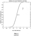
- Fig. 2 illustrates a normalized light transmission response 50 at a particular wavelength of light for an EML as a function of applied voltage for a prior art EAM section of an EML optimized to operate at room temperature.
- room temperature we mean an ambient room temperature that is approximately 25°C.
- the applied voltage is a reverse bias voltage that generates a reverse bias electric field across the semiconductor layer of the EAM.
- the reverse bias electric field causes the absorption edge of the semiconductor material to shift to a longer wavelength (i.e.,a lower absorption edge).
- the shift in the absorption edge causes the semiconductor layer to absorb at least a portion of the light transmitted from the laser diode. Removal or cancellation of all or a substantial part of the reverse bias voltage results in the absorption edge shifting back to a shorter wavelength.
- the normalized light transmission response 50 is for an EAM semiconductor structure that is designed to be substantially transparent to the light emitted by the laser diode with an EAM at substantially zero bias (i.e., no applied bias voltage across the semiconductor layer of the EAM).
- substantially zero bias i.e., no applied bias voltage across the semiconductor layer of the EAM.
- a reverse bias is applied across the semiconductor layer, the absorption edge of the EAM semiconductor layer is shifted to a longer wavelength and, consequently, the EAM begins to absorb a portion of the light transmitted from the laser diode.
- Fig. 2 illustrates that, when the reverse bias is approximately 2 volts in magnitude, the EAM semiconductor layer absorbs substantially all of the light and essentially no light is transmitted from the EML.
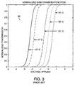
- Fig. 3 illustrates a theoretical family of normalized transmission responses 60 as a function of applied voltage for a prior art electro-absorption modulator.
- the normalized transmission responses 60 are illustrated for five temperatures ranging from -10°C to +45°C. This temperature range represents a portion of the 0 - 65 °C case temperature range specification found in the Multi-Source Agreement (MSA) Reference Document for 300 pin 10 Gb Transponder.
- MSA Multi-Source Agreement
- the theoretical family of normalized transmission responses 60 indicates that in order to achieve a particular normalized transmission level, the magnitude of the required reverse bias voltage across the semiconductor layer decreases as the ambient temperature increases.
- the theoretical family of normalized transmission responses 60 indicates that prior art EAMs, which are optimized to operate at room temperature (approximately 25°C), would require a positive voltage to cause the EAM to absorb light.
- generally semiconductor EAMs cannot reliably operate with positive voltages (substantially greater than 0.5 volts).
- Semiconductor EAMs typically require a reverse bias voltage across the semiconductor layer to move the absorption edge to a longer wavelength thus causing the EAM to absorb the light emitted from the laser diode. Therefore, the theoretical family of normalized transmission responses 60 indicates that prior art EAMs do not function suitably (i.e. absorb light) at temperatures substantially greater than room temperature.
- an EAM can be constructed to achieve a wide operating temperature range by designing the semiconductor layer of the EAM so that a substantially zero (meaning zero or slightly positive voltage, for instance, +0.5 volts) or reverse bias voltage applied across the semiconductor layer causes substantially all light propagating from the laser diode to transmit through the EAM at relatively high operating temperatures or at the maximum operating temperature of the EAM.
- a substantially zero meaning zero or slightly positive voltage, for instance, +0.5 volts
- reverse bias voltage applied across the semiconductor layer causes substantially all light propagating from the laser diode to transmit through the EAM at relatively high operating temperatures or at the maximum operating temperature of the EAM.
- This is achieved, in one embodiment, by engineering the semiconductor layer to be substantially transparent to light propagating through the semiconductor layer when a substantially zero or reverse bias voltage is applied across the semiconductor layer at a relatively high operating temperature, for example, 70°C for MSA applications, or a higher temperature for special application.
- Such an EAM is desirable because it can be operated without external cooling for many applications.
- EML or separate laser and EAM would be relatively inexpensive, would consume less power and would require less space compared with known EMLs and separate EAMs.
- an EAM according to the present invention can be used with external cooling if desired.
- Fig. 4A is a diagram of a semiconductor layer material structure 100 before etching and regrowth of a distributed feedback (DFB) laser diode section of an EML according to the present invention.
- the semiconductor layer material structure 100 comprises a multi-quantum well structure. Multiple quantum well structures are often used in semiconductor laser diode regions because they provide high gain and, consequently, low threshold current and high emission power.
- the quantum well thickness and composition is chosen so that the peak of the gain is at or close to the desired operating wavelength and the periodicity of the underlying structure is chosen so that the laser emission is at the desired wavelength.
- the semiconductor layer material structure 100 is a strained layer (SL) multiple quantum well structure.
- the strained layer reduces the effective mass of the top-most valence sub-band.
- Strained multiple quantum well layers have numerous advantages over unstrained multiple quantum well layers. For example, the use of strained multiple quantum well layers results in better carrier confinement, which reduces the threshold current of the laser. Strained multiple quantum well layers also result in a relatively high differential gain compared with unstrained multiple quantum well layers. In addition, strained multiple quantum well layers have relatively low Auger recombination, which improves efficiency. Furthermore, the strain multiple quantum well layers have a smaller fill-in-factor that can result in a higher saturation optical power level in the optical cavity. The higher saturation optical power level optimizes the laser for moderate to high power operation, which is desirable for some telecommunication applications.
- EMLs are typically optimized for use in optical fiber communication systems, such as wavelength division multiplexed (WDM) optical communication systems.
- WDM wavelength division multiplexed
- the performance of these EMLs can be significantly affected by feedback from the EAM section of the EML to the laser diode section of the EML. This feedback can cause a chirp in the lasing wavelength.
- the feedback may be optical, electrical or a combination of optical and electrical feedback.
- the optical isolation between the laser diode section and the EAM section of the EML is sufficiently high to minimize the feedback from the emitting facet of the EAM section to the laser diode section of the EML.
- the optical isolation between the laser diode section and the EAM section of the EML may be greater than 30 dB.
- a grating isolation section is used to improve the optical isolation.
- an attenuation section is used to improve the optical isolation.
- the grating isolation and attenuation sections generally add optical loss that reduces the optical power emitted from the EML.
- the grating isolation section and attenuation section are designed to minimize the loss.
- the DFB laser is designed to emit relatively narrow emission spectra compared with Fabry-Perot cavity lasers. Narrower emission spectra can be achieved by choosing the appropriate parameters for the DFB grating. In one embodiment, the grating is positioned at an angle relative to the optical waveguide in order to improve stability of the emission wavelength. Such a structure can result in high power lasers having relatively narrow linewidths.
- the semiconductor layer material structure 100 is grown using multi-step metal-organic chemical vapor deposition (MOCVD) growth. However, other known methods of crystal growth can be used to grow the material structure 100.
- the semiconductor layer material structure 100 is grown on an indium phosphide (InP) substrate 102.
- the DFB grating can be fabricated on the substrate 102 before the initial growth or can be fabricated on the top surface after the first re-growth.
- Fig. 4A illustrates a material structure 100 that includes an n-doped InP 103 cladding layer that is grown on the InP substrate 102.
- the lower waveguiding layer 104 is an n-doped InGaAsP layer 104 that has a bandgap of 1.10 ⁇ m.
- the material structure 100 includes an active layer 106 comprising compressive strained multiple quantum well (CSMQWs) layers.
- CSMQWs compressive strained multiple quantum well
- 7.5nm-thick strained quantum wells provide stable light output versus current characteristics at elevated temperature substantially greater than 35 °C, at a wavelength of 1.31 ⁇ m.
- the upper waveguiding layer 108 has substantially the same bandgap as the lower waveguiding layer 104.
- the material structure 100 also includes a p-doped InP 109 cladding layer.
- Fig. 4b illustrates a diagram of one embodiment of a semiconductor layer material structure 100 after etching and regrowth of a distributed feedback (DFB) laser diode section of an EML according to the present invention.
- a narrow mesa is etched using etching techniques that are well known in the art.
- the material structure 100 is then prepared for LP-MOCVD regrowth.
- the first regrowth layers include current confinement layers that are grown on both sides of the mesa.
- the current confinement layers 110, 112, 114 provide lateral current confinement so that the majority of the injected current flows through the multiple quantum well layers 106 ( Fig. 4A ).
- the current confinement layers include n-doped InP 110/p-doped InGaAsP 112 /n-doped InP 114 layers.
- the first regrowth layers also include an InGaAsP layer 112 that is grown on top of the current confinement layer 110.
- the InGaAsP layer 112 has a bandgap wavelength that is approximately 1.2 ⁇ m.
- the InGaAsP layer 112 provides a lateral optical index profile that is suitable for stable single mode operation.
- the second regrowth layers include a p-doped InP layer 116 and a p-InGaAs layer 118.
- the second regrowth layers planarize the semiconductor material structure 120 after the first regrowth.
- the second regrowth layers provide a broad area for a low resistance electrical contact.
- the second regrowth layers provide a good thermal contact.
- the quaternary layers 104 ( Fig. 4A ), 108 ( Fig. 4A ), and 112 ( Fig. 4B ) are grown by low-pressure metal organic vapor phase deposition (LP-MOCVD). Interdiffusion across the interface during MOCVD growth is significantly reduced because the quantum wells and the barrier layers in the active layer 106 ( Fig. 4A ) contain the same elements. Interdiffusion is further reduced when these layers are grown at relatively low temperatures (for example, approximately 550-600°C). In one embodiment, a change of composition is achieved by adjusting the flow rate of the gaseous Group V compounds.
- LP-MOCVD low-pressure metal organic vapor phase deposition
- the material structure of the EAM section of EML is similar to the material structure 100 described in connection with Figs. 4A and 4B .
- the multi-quantum well structure of the EAM section is designed so that the bandgap energy of the material corresponds to a wavelength that is shorter than the lasing wavelength of the DFB laser.
- the absorption in the multi-quantum well region is primarily due to excitonic effects, which results in a relatively sharp absorption edge compared with bulk semiconductor layers. As a result, larger field effects occur over a narrow wavelength range, which increases the temperature sensitivity of the EAM with wavelength compared with bulk semiconductor layers.
- the semiconductor layer material structure of an EAM according to the present invention has a tensile strain in the multi-quantum well region that reduces the temperature sensitivity with wavelength.
- the tensile strain causes splitting of the valence sub-bands and a reduction of the heavy hole mass.
- the EAM is designed to operate at substantially 1310nm and the semiconductor layers of the EAM include 0.4 % tensile-strained quantum wells with a zero-electric-field absorption edge at approximately 1.26 ⁇ m.
- the active region is cladded by two InGaAsP layers to form a relatively large optical cavity waveguide.
- the semiconductor layer of the EAM of the present invention is also designed to have a relatively low voltage sensitivity with respect to wavelength.
- Numerous other semiconductor layer material structures can be used with an EAM and EML according to the present invention.
- numerous other types of semiconductor laser diode regions can be used with the EML of the present application.
- any type of laser emitting light at the desired wavelength can be used with the EML and EAM of the present invention.
- the present invention also features an electronic control circuit that compensates for the inherent temperature drift in performance of an EAM or EML over a wide temperature range.
- the control circuit changes at least one of the EAM DC bias voltage, the peak-to-peak voltage amplitude of the modulation signal, and the laser bias current as functions of operating temperature to allow the EML or separate laser and EAM to operate over a wide operating temperature range.
- Fig. 5 illustrates a functional block diagram of an electro-absorption modulated laser (EML) 200 and control circuit 202 according to one aspect of the present invention.
- the EML 200 includes a laser diode 204 section and an electro-absorption modulator (EAM) 206 section.
- the laser diode 204 is a distributed feedback (DFB) laser and the EAM 206 comprises a multi-quantum well device that includes the material structure described in connection with Figs. 4A and 4B .
- the leaser diode 204 and EAM 206 are integrated onto a single substrate.
- the laser diode 204 and EAM 206 are physically separate devices.
- the EML 200 can include a thermoelectric cooler 205 that is in thermal communication with the laser diode 204.
- the thermoelectric cooler 205 can be used to control the temperature of the laser diode 204 in order to change the wavelength of the light generated by the laser diode 204.
- a temperature rise of 10°C (from, for example, room temperature) in a typical DFB laser diode can cause the wavelength of the emission to increase by approximately 1nm.
- the control circuit 202 includes an electronic laser drive circuit 202', or bias control circuit, that is electrically coupled to a bias input 208 of the laser diode 204.
- the electronic laser drive circuit 202' generates a continuous wave (CW) current that drives the laser diode 204 causing it to emit photons.
- the control circuit 202 also includes an amplitude control circuit 202" that is electrically connected to the laser drive circuit 202'. The amplitude control circuit 202" controls the amplitude of the CW current that is generated by laser drive circuit 202'.
- a temperature sensor 209 is positioned in thermal communication with the laser diode 204.
- the output of the temperature sensor 209 is electrically connected to an input 209' of the amplitude control circuit 202.”
- the temperature sensor 209 generates a signal at the output that is related to the temperature of the laser 204.
- the amplitude control circuit 202" is slaved to the temperature of the laser 204.
- the amplitude control circuit 202" receives the signal generated by the temperature sensor 209 at the input 209' and generates a signal that instructs the electronic laser drive circuit 202' to change the CW current that drives the laser diode 204 in response to the measured temperature so as to control the wavelength of the light emitted by the laser diode 204.
- the optical power emitted from the laser diode 204 is monitored by an optical power detector 210 that is positioned in optical communication with the back facet 212 of the laser diode 204.
- an optical power detector (not shown) is in optical communication with the front facet 212' of the laser diode 204.
- the optical power detector 210 generates an electrical signal that is related to the optical power emitted by the laser diode 204 that propagates into the EAM 206.
- the amplitude control circuit 202" has an input 203 that is electrically connected to the output of the optical power detector 210.
- the amplitude control circuit 202" generates a signal that instructs the laser drive circuit 202' to generate a CW current having a predetermined amplitude in response to the optical power emitted from the laser diode 204.
- An electronic data modulation circuit 214 is electrically coupled to a modulation input 216 of the EAM 206.
- the electronic data modulation circuit 214 is capacitively coupled to the modulation input 216 of the EAM 206 by a capacitor 219.
- the electronic data modulation circuit 214 generates a modulation signal that reverse biases the EAM 206 and causes the EAM 206 to modulate the light emitted from the laser diode 204 that propagates into the EAM 206 by either transmitting the light through the EAM 206 or by absorbing the light within the EAM 206.
- the control circuit 202 also includes an EAM DC bias voltage control circuit 202'" that is electrically connected to a control input 217 of the data modulation circuit 214.
- a temperature sensor 218 is positioned in thermal communication with the EAM 206. The temperature sensor 218 generates a signal at an output that is related to the temperature of the EAM 206.
- the EAM DC bias voltage control circuit 202'" includes an input 220 that is electrically coupled to the output of the temperature sensor 218. In this embodiment, the EAM DC bias voltage control circuit 202'" is slaved to the temperature of the EAM 206.
- the EAM DC bias voltage control circuit 202'" receives the signal generated by the temperature sensor 218 at the input 220 and generates a signal that instructs the data modulation circuit 214 to change the DC bias voltage applied to the EAM 206 in response to the measured temperature so as to control the absorption edge of the EAM 206.
- the light modulated by the EAM 206 is emitted at an optical output 222 of the EML 200,
- the optical output 222 may be directly coupled to an optical transport medium (not shown), such as an optical fiber, a lens transport system or free space.
- the wavelength of the modulated light is controlled by adjusting the CW current generated by the laser drive circuit 202' and applied to the bias input 208 of the laser diode 204.
- the wavelength of the modulated light can also be controlled by adjusting the temperature of the laser diode 204.
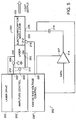
- Fig. 6 illustrates a functional block diagram of one embodiment of a control circuit 250 of an EML 252 according to the present invention.
- the control circuit 250 includes a laser diode driver circuit 254 and an EAM driver circuit 256.
- the EAM driver circuit 256 includes a thermal sensor 258 that measures the temperature of the laser diode 260 in the EML 252.
- the thermal sensor 258 generates a signal having a voltage that is proportional to the temperature of the laser diode 260.
- An amplifier 262 amplifies the signal generated by the thermal sensor 258 to a signal level that can be easily processed.
- a processor 264 which can include a look-up table, receives the amplified signal from the amplifier 262 at an input 266.
- the control circuit 250 includes an EAM driver 268 that has an input 270 that is electrically connected to an output 272 of the processor 264 so that a DC bias voltage, V DC Bias can be applied to the EAM driver 268.
- the EAM driver 268 has an output 274 that is electrically connected to the EAM 261.
- the processor 264 uses the look-up table to determine the appropriate DC bias voltage for the EAM 261.
- the processor 264 generates a signal that instructs the EAM driver 268 to generate the appropriate DC bias voltage.
- the laser diode driver circuit 254 includes a set-point voltage circuit 276 and a laser diode driver 278.
- the set-point voltage circuit 276 can be a voltage comparator.
- an optical detector 280 is optically coupled to the back or front facet of the laser diode 260.
- the optical detector 280 generates a monitor current (Iph).
- a circuit 282 is electrically connected to the output of the optical detector 280 and converts the monitor current (Iph) to a reference voltage.
- the output of the circuit 282 is electrically connected to one input of the set-point voltage circuit 276.
- the set-point voltage circuit 276 is a voltage comparator.
- the set-point voltage circuit 276 compares the reference voltage to a set-point voltage applied to another input of the set-point voltage circuit 276 (and in particular, in the embodiment shown, to the non-inverting input of the comparator) and generates a control signal at an output 284 that is a function of a comparison of the two input signals.
- the laser diode driver 278 is electrically connected to the output 284 of the set-point voltage circuit 276.
- the laser diode driver 278 includes an opamp (Ul) and a transistor (Q1).
- the laser diode driver 278 receives the control signal at an input 286 and generates a laser drive current.
- the set-point voltage can be adjusted to adjust the drive current of the laser diode 260 to meet the power output requirements of the EML 252.
- the control circuit 250 can be used to drive the EML 252 so that the EML 252 generates an optical signal that has a substantially optimal transmitter eye pattern over the entire temperature operating range of approximately 0°C to 70°C for MSA applications, or a higher temperature for special applications.
- the control circuit 250 of the present invention can be practiced with many other known configurations.
- Fig. 7 illustrates a family of normalized transmission responses 300 for a particular operating wavelength over a range of temperatures as a function of applied voltage for one embodiment of an EAM according to the present invention.
- the EAM material structure for this embodiment is designed as described herein to operate with an applied reverse bias voltage through the entire operating temperature range up to the maximum temperature requirement of 70°C for MSA applications, or a higher temperature for special application.
- the transmission responses 300 of the EAM according to the present invention indicate wavelength shifts that are approximately 0.59nm/°C at an operating wavelength of approximately 1310nm.
- the transmission responses 300 also indicate wavelength shifts that are approximately 41.3nm over a temperature range of 70°C for MSA applications.
- a DFB laser with a wavelength shift of approximately 0.08nm/°C will exhibit a total wavelength shift over of approximately 5.6nm over the 70°C operating temperature range of approximately 0°C to 70°e.
- both devices will experience a positive wavelength shift with temperature. Therefore, the differential shift for the integrated EML including both the EAM and the DBF laser will be approximately 35.7nm (41.3nm-5.6nm) over a 70°C operating temperature range (from approximately 0°C to 70°C). Data also indicates that the EAM can be tuned by 21 nm with 2V of reverse bias voltage applied. Therefore, the entire range of the temperature from 0°C to 70°C can be compensated with an electronic control circuit that provides a range of approximately 3.4V of reverse bias to the EAM, i.e., approximately OVDC to approximately -3.4VDC.
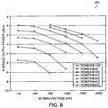
- Fig. 8 illustrates experimental data 350 for output power as a function of EAM bias voltage and operating temperature for an EML according to the present invention.
- the bias voltage ranges from ⁇ 0V to -2V for several operating temperatures.
- An EML according to the present invention can operate within the MSA operating temperature specifications without the use of an external cooling element, such as a thermoelectric cooler. Such an EML is advantageous because external cooling increases the power and space requirements, and adds to the cost of the device.
- EMLs using a control circuit according to the present invention have achieved performance that meets the SONET signal "eye" requirements over a 47°C temperature range of -7°C to 40°C (the lower temperature of -7°C was limited by test equipment).
- An EML with a material structure engineered according to the present invention and using a control circuit according to the present invention can also be used to achieve temperature stability performance over 0 °C to 70 °C for MSA applications, or a higher temperature for special application.
- an EAM according to the present invention can be used with any type of laser and is not limited to the use with a DFB semiconductor laser diode.
Landscapes
- Physics & Mathematics (AREA)
- Optics & Photonics (AREA)
- Engineering & Computer Science (AREA)
- Chemical & Material Sciences (AREA)
- General Physics & Mathematics (AREA)
- Nonlinear Science (AREA)
- Nanotechnology (AREA)
- Crystallography & Structural Chemistry (AREA)
- Condensed Matter Physics & Semiconductors (AREA)
- Electromagnetism (AREA)
- Biophysics (AREA)
- Life Sciences & Earth Sciences (AREA)
- Optical Modulation, Optical Deflection, Nonlinear Optics, Optical Demodulation, Optical Logic Elements (AREA)
- Semiconductor Lasers (AREA)
- Electrochromic Elements, Electrophoresis, Or Variable Reflection Or Absorption Elements (AREA)
- Optical Integrated Circuits (AREA)
Description
- This patent application claims priority to provisional patent application Serial No.
60/304,496, filed on July 11, 2001 - The present invention relates generally to optical modulators and to modulated lasers. In particular, the present invention relates to methods and apparatus for modulating light with an electro-absorption modulator.
- Electro-absorption modulators (EAMs) and electro-absorption modulated lasers (EMLs) are useful for transmitting information in telecommunications or data communication systems. EMLs have several advantages over other modulation sources. For example, EMLs can directly generate communication signals with relatively low bit-terror rates without the use of external filters, which are undesirable because they are relatively large and expensive. External filters also occupy valuable space on the transmitter electronics board. In addition, EMLs directly generate transmission characteristics that have a relatively "clean" eye pattern when viewed on a communication signal analyzer. Such an eye pattern indicates acceptable discrimination between a digital "1" and digital "0" and, therefore, a relatively error-free (i.e. a bit error rate of less than 10-9) information transmission.
- Another advantage of EMLs is that they can generate a stable and high-power modulated light beam. Yet another advantage of EMLs is that they can generate optical signals that are modulated at relatively high data rates. In addition, an EML is convenient to use because it is relatively easy to mount an EML in a package with an industry standard input impedance, which can be impedance matched to numerous commercially available drive voltage sources. EMLs are also relatively inexpensive.
- A disadvantage of common, currently available EMLs, however, is that they require external thermal controllers for many practical applications. For example, EMLs require external thermal controllers, such as thermoelectric coolers (TECs), to maintain the EMLs at a substantially constant operating temperature so that data transmission can occur relatively error-free even as ambient temperatures vary over a relatively large,range, e. g. , over the entire Synchronous Optical Network (SONET) standardized operating temperature range. In general, external thermoelectric coolers are undesirable because they are power-intensive, relatively large and relatively expensive devices.
- "3.2 nm wavelength tuning via temperature control for integrated electro absorption modulator/DFB laser with high tolerance to chromatic dispersion", B. Clesca et al, Electronics Letters, vol. 32, No. 10 pages 927-929, which refers to "2.5-Gbit/s, 1291-km transmission over non-dispersion-shifted fibre using an integrated electroabsorption modulator/DFB laser module", B. Clesca et al, Proceedings of the 21st European conference on optical communications (ECOC'95), 1995, pages 995-998 together describe an electroabsorption modulated laser with 3.2 nm wavelength tuning via temperature control with bias and driving voltages adjusted according to temperature in order to maintain the extinction ratio.
- The present invention relates to electro-absorption modulators (EAMs) and electro-absorption modulated lasers (EMLs) with high operating temperature tolerance. An EAM and EML according to the present invention can operate without external thermal controllers, such as TECs, and thus can require less power and less space than known EAMs and EMLs. However, the methods and apparatus of the present invention can be practiced with or without external temperature control.
- Accordingly, the present invention features an EAM that includes as semiconductor layer having an electrically controllable light absorption. In one embodiment, the semiconductor layer is a multi-quantum well layer. In another embodiment, the semiconductor layer is a bulk semiconductor layer. The material composition of the semiconductor layer is chosen so that the semiconductor layer is transparent to light propagating through the semiconductor layer when a substantially zero or a reverse bias voltage is applied across the semiconductor layer at operating temperatures of the electro-absorption modulator that are greater than 25 degrees Celsius, and wherein the modulator further comprises current confinement layers that provide lateral current confinement that, in use, result in a majority of the injected current flowing through the semiconductor layer. The material composition of the semiconductor layer may be chosen to modulate light that is substantially 1310nm or that is substantially 1550nm.
- In another embodiment, the material composition is chosen so that the semiconductor layer is substantially transparent to light propagating through the semiconductor layer when a substantially zero or a reverse bias voltage is applied across the semiconductor layer at operating temperatures of the electro-absorption modulator that are substantially greater than 35 degrees Celsius. In another embodiment, the material composition is chosen so that the semiconductor layer is substantially transparent to light propagating through the semiconductor layer when a substantially zero or a reverse bias voltage is applied across the semiconductor layer at operating temperatures of the electro-absorption modulator that are substantially greater than 45 degrees Celsius.
- In yet another embodiment, the material composition is chosen so that the semiconductor layer is substantially transparent to light propagating through the semiconductor layer when a substantially zero or a reverse bias voltage is applied across the semiconductor layer at the maximum operating temperature of the electro-absorption modulator.
- An electronic data modulator may be electrically coupled to the electro-absorption modulator. An output of the electronic data modulator is electrically coupled to a modulation input of the electro-absorption modulator. The electronic data modulator generates an electrical modulation signal having a peak-to-peak voltage amplitude that changes the absorption edge of the semiconductor layer, thereby changing the light transmission characteristics of the electro-absorption modulator.
- The modulation signal turns the EAM from optically transparent to optically opaque with an applied reverse bias voltage. The amplitude of the desired peak-to-peak voltage of the modulation signal (approximately 1 to 2.5 volts) changes with temperature as the EAM absorption changes as a function of temperature. The amplitude of the peak-to-peak voltage of the modulation signal depends on the desired light extinction characteristics. For example, to achieve an extinction ratio of about 13dB, a peak-to-peak amplitude of between 1 to 2.5 volts at room temperature is required for some known materials.
- A temperature-driven controller is used. A temperature sensor is positioned in thermal communication with the semiconductor layer of the electro-absorption modulator (and optionally an active layer of a semiconductor laser that generates the light that propagates through the semiconductor layer of the EAM). The temperature- driven controller has an input that is electrically coupled to the thermal sensor and an output that is electrically coupled to a DC bias control input of the electronic data modulator.
- The temperature-driven controller generates a signal that changes the DC bias of the electrical modulation signal generated by the electronic data modulator. The temperature-driven controller may include a processor that includes a look-up table that is used to determine various parameters, such as the desired DC bias voltage across the semiconductor layer for a particular temperature.
- The present invention also features an electro-absorption modulated laser (EML) that includes a laser that generates light at an output. In one embodiment, the laser is a distributed feedback semiconductor laser. In one embodiment, a thermoelectric cooler is positioned in thermal communication with the laser. The thermoelectric cooler may be used to change a wavelength of the light generated by the laser. In one embodiment, the wavelength of the light generated by the laser is substantially 1310 nm or is substantially 1550 nm.
- The electro-absorption modulated laser also includes an electro-absorption modulator that modulates the light generated by the laser. The laser and the electro-absorption modulator may be integrated onto a single substrate or may be physically separate devices.
- The electro-absorption modulator includes a semiconductor layer having an electrically controllable absorption. The semiconductor layer may be a multi-quantum well layer or a bulk semiconductor layer. The material composition of the semiconductor layer is chosen so that the semiconductor layer is substantially transparent to light propagating through the semiconductor layer when a substantially zero or a reverse bias voltage is applied across the semiconductor layer at operating temperatures of the electro-absorption modulator that are substantially greater than 25 degrees Celsius. The material composition of the semiconductor layer may be chosen to modulate light that is substantially 1310 nm or that is substantially 1550 nm.
- In one embodiment, the material composition of the electro-absorption modulator is chosen so that the semiconductor layer is substantially transparent to light propagating through the semiconductor layer when a substantially zero or a reverse bias voltage is applied across the semiconductor layer at the maximum operating temperature of the electro-absorption modulator.
- The present invention also features a transmitter for an optical communication system or a transponder that includes a transmitter. In one embodiment, the transmitter generates optical signals having a wavelength that is substantially 1310 nm or substantially 1550 nm. In another embodiment, the transmitter generates optical signals at any desired communication wavelength for transmission via optical fiber or through the atmosphere.
- The transmitter includes a laser that generates light at an output. The transmitter also includes an electro-absorption modulator with a semiconductor layer having an electrically controllable absorption. The material composition of the semiconductor layer is chosen so that the semiconductor layer is substantially transparent to light propagating through the semiconductor layer when a substantially zero or a reverse bias voltage is applied across the semiconductor layer at operating temperatures of the electro-absorption modulator that are substantially greater than 25 degrees Celsius.
- An electronic data modulator modulates the light generated by the laser. The electronic data modulator has an output that is electrically coupled to a modulation input of the electro-absorption modulator. The electronic data modulator generates an electrical modulation signal having a peak-to-peak voltage amplitude that changes the absorption edge of the semiconductor layer, thereby changing the light transmission characteristics of the electro-absorption modulator.
- A temperature sensor is positioned in thermal communication with at least one of the semiconductor laser and the semiconductor layer of the electro-absorption modulator. The transmitter includes a temperature-driven controller that has an input that is electrically coupled to the thermal sensor and an output that is electrically coupled to a DC bias control input of the electronic data modulator.
- The temperature-driven controller generates a signal that changes the DC bias of the electrical modulation signal generated by the electronic data modulator. The temperature-driven controller may include a processor that includes a look-up table that is used to determine various parameters, such as the desired DC bias voltage across the semiconductor layer for a particular temperature.
- The present invention also features a method of generating data modulated light: The method includes generating light and then propagating the light through an electro-absorption modulator comprising a semiconductor layer having an electrically controllable absorption. The semiconductor layer has a material composition that is chosen so that the semiconductor layer is transparent to light propagating though the semiconductor layer when a substantially zero or a reverse bias voltage is applied across the semiconductor layer at operating temperatures of the electro-absorption modulator that are greater than 25 degrees Celsius and wherein the modulator further comprises current confinement layers that provide lateral current confinement that, in use, result in a majority of the injected current flowing through the semiconductor layer.
- The method also includes elevating the temperature of the semiconductor layer above 25 degrees Celsius. A DC reverse bias voltage is applied across the semiconductor layer. A modulation signal having a voltage is applied across the semiconductor layer. The modulation signal changes an absorption edge of the semiconductor layer, thereby modulating the light.
- The temperature of the semiconductor layer (and optionally a laser that generates the light) is measured, and the DC bias voltage applied across the semiconductor layer is changed in response to the measured temperature. In another embodiment, the temperature of the semiconductor layer or a laser that generates the light is measured, and the bias current driving a laser that generates the light is changed in response to the measured temperature.
- The present invention also features a method of tracking a temperature of an electro-absorption modulator to a temperature of a semiconductor laser. The method includes generating light with a semiconductor laser. The light is propagated through an electro-absorption modulator comprising a semiconductor layer having an electrically controllable absorption. The semiconductor layer has a material composition that is chosen so that the semiconductor layer is substantially transparent to light propagating through the semiconductor layer when a substantially zero or a reverse bias voltage is applied across the semiconductor layer at operating temperatures of the electroabsorption modulator that are substantially greater than 25 degrees Celsius.
- A modulation signal having a peak-to-peak voltage amplitude of, for example, 1.0 to 2.5 volts, is applied across the semiconductor layer. The modulation signal changes the absorption edge of the semiconductor layer, thereby changing the light transmission characteristics of the electro-absorption modulator and modulating the light generated by the laser. The temperature of the laser that generates the light is measured and the peak-to-peak voltage amplitude of the electrical modulation signal is changed in response to the measured temperature so that a desired extinction ratio of the transmitted light is attained. By extinction ratio we mean:

- This invention is described with particularity in the below description. The above and further advantages of this invention may be better understood by referring to the following description in conjunction with the accompanying drawings, in which like numerals indicate like structural elements and features in various figures. The drawings are not necessarily to scale, emphasis instead being placed upon illustrating the principles of the invention. Preferred embodiments of the invention will now be described, by way of example only, and with reference to the accompanying drawings in which:
-
Fig. 1 illustrates a typical prior art electro-absorption modulated laser. -
Fig. 2 illustrates a normalized light transmission response for a particular operating wavelength of light as a function of applied voltage for a prior art EAM section of an EML that is optimized to operate at room temperature. -
Fig. 3 illustrates a theoretical family of normalized transmission responses as a function of applied voltage for a prior art electro-absorption modulator at five different temperatures. -
Fig. 4A is a diagram of one embodiment of a semiconductor layer material structure before etching and regrowth of a typical distributed feedback laser diode section of an EML according to the present invention. -
Fig. 4B illustrates a diagram of one embodiment of a semiconductorlayer material structure 100 after etching and regrowth of a distributed feedback (DFB) laser diode section of an EML according to the present invention. -
Fig. 5 illustrates a functional block diagram of an electro-absorption modulated laser and control circuit according to the present invention. -
Fig. 6 illustrates a functional block diagram of one embodiment of a control circuit of an electro-absorption modulated laser according to the present invention. -
Fig. 7 illustrates a family of theoretical normalized transmission responses as a function of applied voltage at various operating temperatures for one embodiment of an electro-absorption modulator according to the present invention. -
Fig. 8 illustrates experimental data for output power as a function of bias voltage at various operating temperatures for one embodiment of an electro-absorption modulated laser according to the present invention. -
Fig. 1 illustrates a prior art electro-absorption modulated laser (EML) 10. TheEML 10 includes alaser diode 12 section and an electro-absorption modulator (EAM) 14 section. Thelaser diode 12 section is typically a distributed feedback (DFB) laser. TheEAM 14 is typically a device that includes a semiconductor layer, such as a multi-quantum well semiconductor layer. The semiconductor layer typically has a slightly larger bandgap than the photon energy of the light being modulated. Thelaser diode 12 section is optically coupled to theEAM 14 section. Thelaser diode 12 section andEAM section 14 are typically integrated onto a single substrate, but can be physically separate devices. - An electronic
laser drive circuit 16 is electrically coupled to abias input 18 of thelaser diode 12. The electroniclaser drive circuit 16 generates a continuous wave (CW) current that drives thelaser diode 12, thereby causing thelaser diode 12 to emit substantially monochromatic light of a predetermined wavelength. An electronicdata modulation circuit 20 is electrically coupled to amodulation input 22 of theEAM 14. - The electronic
data modulator circuit 20 generates a voltage across the multi-quantum well semiconductor layer that produces a reverse bias electric field across the semiconductor layer. The reverse bias electric field causes the absorption edge of the semiconductor layer to reversibly move to a longer wavelength (i.e., the reverse bias field lowers the absorption edge). The shift in the absorption edge causes the semiconductor layer to absorb the light generated by thelaser diode 12 section that propagates through the semiconductor layer. - Reducing the voltage across the multi-quantum well semiconductor layer results in the elimination or reduction of the reverse bias electric field, which in turn causes the semiconductor layer to allow light generated by the
laser diode 12 to transmit through the semiconductor layer. Therefore, light emitted from thelaser diode 12 that propagates to theEAM 14 can be modulated by modulating the voltage across the multi-quantum well semiconductor layer between a sufficient reverse bias voltage across the semiconductor layer that causes the layer to be substantially opaque to the light emitted from thelaser diode 12, and substantially zero or a sufficiently positive bias voltage that causes the layer to be substantially transparent to the light emitted from thelaser diode 12. - The resulting modulated light is emitted at an
optical output 24 of theEML 10. Theoptical output 24 can be directly coupled to an optical transport medium (not shown), such as an optical fiber, or can be coupled to an optical transport medium through a lens transport system. The wavelength of the modulated light can be controlled by adjusting the amplitude of the CW current generated by the electroniclaser drive circuit 16 and applied to thelaser diode 12. The wavelength of the modulated light can also be controlled by adjusting the temperature of thelaser diode 12. - Common
prior art EML 10 devices include a thermoelectric cooler (TEC) 26 that controls the temperature of thelaser diode 12 andEAM 14. The temperature of theEML 10 can be stabilized by using athermal sensor 28 and afeedback circuit 30. Thethermal sensor 28 is thermally coupled to thelaser diode 12 and is electrically coupled to afeedback circuit 30 at aninput 32. Thefeedback circuit 30 is electrically coupled to theTEC 26 at aninput 34. Thefeedback circuit 30 receives a signal from thethermal sensor 28 at theinput 32 that is related to the measured temperature of thelaser diode 12 and generates a signal at anoutput 36 in response to the measured temperature. The signal generated by thefeedback circuit 30 controls the thermal properties of theTEC 26 to maintain thelaser diode 12 at a predetermined operating temperature (and thus the major portion of spectral energy of the emitted light at the desired wavelength) independent of ambient temperature. -
Fig. 2 illustrates a normalizedlight transmission response 50 at a particular wavelength of light for an EML as a function of applied voltage for a prior art EAM section of an EML optimized to operate at room temperature. By room temperature, we mean an ambient room temperature that is approximately 25°C. The applied voltage is a reverse bias voltage that generates a reverse bias electric field across the semiconductor layer of the EAM. The reverse bias electric field causes the absorption edge of the semiconductor material to shift to a longer wavelength (i.e.,a lower absorption edge). The shift in the absorption edge causes the semiconductor layer to absorb at least a portion of the light transmitted from the laser diode. Removal or cancellation of all or a substantial part of the reverse bias voltage results in the absorption edge shifting back to a shorter wavelength. - The normalized
light transmission response 50 is for an EAM semiconductor structure that is designed to be substantially transparent to the light emitted by the laser diode with an EAM at substantially zero bias (i.e., no applied bias voltage across the semiconductor layer of the EAM). When a reverse bias is applied across the semiconductor layer, the absorption edge of the EAM semiconductor layer is shifted to a longer wavelength and, consequently, the EAM begins to absorb a portion of the light transmitted from the laser diode.Fig. 2 illustrates that, when the reverse bias is approximately 2 volts in magnitude, the EAM semiconductor layer absorbs substantially all of the light and essentially no light is transmitted from the EML. -
Fig. 3 illustrates a theoretical family of normalizedtransmission responses 60 as a function of applied voltage for a prior art electro-absorption modulator. The normalizedtransmission responses 60 are illustrated for five temperatures ranging from -10°C to +45°C. This temperature range represents a portion of the 0 - 65 °C case temperature range specification found in the Multi-Source Agreement (MSA) Reference Document for 300pin 10 Gb Transponder. The theoretical family of normalizedtransmission responses 60 indicates that in order to achieve a particular normalized transmission level, the magnitude of the required reverse bias voltage across the semiconductor layer decreases as the ambient temperature increases. - At elevated temperatures (approximately 35°C and above), the theoretical family of normalized
transmission responses 60 indicates that prior art EAMs, which are optimized to operate at room temperature (approximately 25°C), would require a positive voltage to cause the EAM to absorb light. However, generally semiconductor EAMs cannot reliably operate with positive voltages (substantially greater than 0.5 volts). Semiconductor EAMs typically require a reverse bias voltage across the semiconductor layer to move the absorption edge to a longer wavelength thus causing the EAM to absorb the light emitted from the laser diode. Therefore, the theoretical family of normalizedtransmission responses 60 indicates that prior art EAMs do not function suitably (i.e. absorb light) at temperatures substantially greater than room temperature. - Applicants have discovered that an EAM can be constructed to achieve a wide operating temperature range by designing the semiconductor layer of the EAM so that a substantially zero (meaning zero or slightly positive voltage, for instance, +0.5 volts) or reverse bias voltage applied across the semiconductor layer causes substantially all light propagating from the laser diode to transmit through the EAM at relatively high operating temperatures or at the maximum operating temperature of the EAM. This is achieved, in one embodiment, by engineering the semiconductor layer to be substantially transparent to light propagating through the semiconductor layer when a substantially zero or reverse bias voltage is applied across the semiconductor layer at a relatively high operating temperature, for example, 70°C for MSA applications, or a higher temperature for special application.
- Such an EAM is desirable because it can be operated without external cooling for many applications. Thus, such an EML or separate laser and EAM would be relatively inexpensive, would consume less power and would require less space compared with known EMLs and separate EAMs. However, although not required, an EAM according to the present invention can be used with external cooling if desired.
-
Fig. 4A is a diagram of a semiconductorlayer material structure 100 before etching and regrowth of a distributed feedback (DFB) laser diode section of an EML according to the present invention. The semiconductorlayer material structure 100 comprises a multi-quantum well structure. Multiple quantum well structures are often used in semiconductor laser diode regions because they provide high gain and, consequently, low threshold current and high emission power. In one embodiment, the quantum well thickness and composition is chosen so that the peak of the gain is at or close to the desired operating wavelength and the periodicity of the underlying structure is chosen so that the laser emission is at the desired wavelength. - In one embodiment, the semiconductor
layer material structure 100 is a strained layer (SL) multiple quantum well structure. The strained layer has a biaxial strain that causes a splitting of the valence sub-bands. Specifically, the axial component of a hydrostatic strain causes the heavy hole (hh) and the light hole (lh) states to split near the k = 0 point for both tensile-strained (TS) and compressively-strained (CS) multiple quantum wells. The strained layer reduces the effective mass of the top-most valence sub-band. - Strained multiple quantum well layers have numerous advantages over unstrained multiple quantum well layers. For example, the use of strained multiple quantum well layers results in better carrier confinement, which reduces the threshold current of the laser. Strained multiple quantum well layers also result in a relatively high differential gain compared with unstrained multiple quantum well layers. In addition, strained multiple quantum well layers have relatively low Auger recombination, which improves efficiency. Furthermore, the strain multiple quantum well layers have a smaller fill-in-factor that can result in a higher saturation optical power level in the optical cavity. The higher saturation optical power level optimizes the laser for moderate to high power operation, which is desirable for some telecommunication applications.
- Commercial EMLs are typically optimized for use in optical fiber communication systems, such as wavelength division multiplexed (WDM) optical communication systems. The performance of these EMLs can be significantly affected by feedback from the EAM section of the EML to the laser diode section of the EML. This feedback can cause a chirp in the lasing wavelength. The feedback may be optical, electrical or a combination of optical and electrical feedback.
- In one embodiment of the invention, the optical isolation between the laser diode section and the EAM section of the EML is sufficiently high to minimize the feedback from the emitting facet of the EAM section to the laser diode section of the EML. For example, the optical isolation between the laser diode section and the EAM section of the EML may be greater than 30 dB. In one embodiment, a grating isolation section is used to improve the optical isolation. In another embodiment, an attenuation section is used to improve the optical isolation. The grating isolation and attenuation sections generally add optical loss that reduces the optical power emitted from the EML. In one embodiment, the grating isolation section and attenuation section are designed to minimize the loss.
- In one embodiment, the DFB laser is designed to emit relatively narrow emission spectra compared with Fabry-Perot cavity lasers. Narrower emission spectra can be achieved by choosing the appropriate parameters for the DFB grating. In one embodiment, the grating is positioned at an angle relative to the optical waveguide in order to improve stability of the emission wavelength. Such a structure can result in high power lasers having relatively narrow linewidths.
- In one embodiment, the semiconductor
layer material structure 100 is grown using multi-step metal-organic chemical vapor deposition (MOCVD) growth. However, other known methods of crystal growth can be used to grow thematerial structure 100. In one embodiment, the semiconductorlayer material structure 100 is grown on an indium phosphide (InP)substrate 102. The DFB grating can be fabricated on thesubstrate 102 before the initial growth or can be fabricated on the top surface after the first re-growth. - Specifically,
Fig. 4A illustrates amaterial structure 100 that includes an n-dopedInP 103 cladding layer that is grown on theInP substrate 102. Thematerial structure 100 also includes alower waveguiding layer 104 that, in one embodiment, has a 1.1 µm bandgap n-doped In1-xGaxAsyP1-y (x=0.14, y=0.33) quaternary layer that is lattice matched to theInP substrate 102. In one embodiment, thelower waveguiding layer 104 is an n-dopedInGaAsP layer 104 that has a bandgap of 1.10 µm. - In addition, the
material structure 100 includes anactive layer 106 comprising compressive strained multiple quantum well (CSMQWs) layers. For example, a strained In1-xGaxAsyP1-y (x=0.14, y=0.52) layer, which has a material bandgap of 1.42 µm, may be used as the quantum well. For example, 7.5nm-thick strained quantum wells provide stable light output versus current characteristics at elevated temperature substantially greater than 35 °C, at a wavelength of 1.31 µm. - The
material structure 100 also includes anupper waveguiding layer 108 that, in one embodiment, is a 1.1µm bandgap p-doped In1-xGaxAsyP1-y (x=0.14, y=0.33) quaternary layer that is lattice matched to theInP substrate 102. In one embodiment, theupper waveguiding layer 108 has substantially the same bandgap as thelower waveguiding layer 104. Thematerial structure 100 also includes a p-dopedInP 109 cladding layer. -
Fig. 4b illustrates a diagram of one embodiment of a semiconductorlayer material structure 100 after etching and regrowth of a distributed feedback (DFB) laser diode section of an EML according to the present invention. A narrow mesa is etched using etching techniques that are well known in the art. Thematerial structure 100 is then prepared for LP-MOCVD regrowth. The first regrowth layers include current confinement layers that are grown on both sides of the mesa. The current confinement layers 110, 112, 114 provide lateral current confinement so that the majority of the injected current flows through the multiple quantum well layers 106 (Fig. 4A ). In one embodiment, the current confinement layers include n-dopedInP 110/p-dopedInGaAsP 112 /n-dopedInP 114 layers. - The first regrowth layers also include an
InGaAsP layer 112 that is grown on top of thecurrent confinement layer 110. In one embodiment, theInGaAsP layer 112 has a bandgap wavelength that is approximately 1.2 µm. TheInGaAsP layer 112 provides a lateral optical index profile that is suitable for stable single mode operation. - A second regrowth is then performed, as shown in
Fig. 4b . In one embodiment, the second regrowth layers include a p-dopedInP layer 116 and a p-InGaAs layer 118. The second regrowth layers planarize thesemiconductor material structure 120 after the first regrowth. Also, the second regrowth layers provide a broad area for a low resistance electrical contact. In addition, the second regrowth layers provide a good thermal contact. - In one embodiment, the quaternary layers 104 (
Fig. 4A ), 108 (Fig. 4A ), and 112 (Fig. 4B ) are grown by low-pressure metal organic vapor phase deposition (LP-MOCVD). Interdiffusion across the interface during MOCVD growth is significantly reduced because the quantum wells and the barrier layers in the active layer 106 (Fig. 4A ) contain the same elements. Interdiffusion is further reduced when these layers are grown at relatively low temperatures (for example, approximately 550-600°C). In one embodiment, a change of composition is achieved by adjusting the flow rate of the gaseous Group V compounds. - In one embodiment, the material structure of the EAM section of EML is similar to the
material structure 100 described in connection withFigs. 4A and 4B . However, the multi-quantum well structure of the EAM section is designed so that the bandgap energy of the material corresponds to a wavelength that is shorter than the lasing wavelength of the DFB laser. The absorption in the multi-quantum well region is primarily due to excitonic effects, which results in a relatively sharp absorption edge compared with bulk semiconductor layers. As a result, larger field effects occur over a narrow wavelength range, which increases the temperature sensitivity of the EAM with wavelength compared with bulk semiconductor layers. - In one embodiment, the semiconductor layer material structure of an EAM according to the present invention has a tensile strain in the multi-quantum well region that reduces the temperature sensitivity with wavelength. The tensile strain causes splitting of the valence sub-bands and a reduction of the heavy hole mass. For example, in one embodiment, the EAM is designed to operate at substantially 1310nm and the semiconductor layers of the EAM include 0.4 % tensile-strained quantum wells with a zero-electric-field absorption edge at approximately 1.26µm. The active region is cladded by two InGaAsP layers to form a relatively large optical cavity waveguide. In one embodiment, the semiconductor layer of the EAM of the present invention is also designed to have a relatively low voltage sensitivity with respect to wavelength.
- Numerous other semiconductor layer material structures can be used with an EAM and EML according to the present invention. Furthermore, numerous other types of semiconductor laser diode regions can be used with the EML of the present application. In fact, any type of laser emitting light at the desired wavelength can be used with the EML and EAM of the present invention.
- The present invention also features an electronic control circuit that compensates for the inherent temperature drift in performance of an EAM or EML over a wide temperature range. The control circuit changes at least one of the EAM DC bias voltage, the peak-to-peak voltage amplitude of the modulation signal, and the laser bias current as functions of operating temperature to allow the EML or separate laser and EAM to operate over a wide operating temperature range.
-
Fig. 5 illustrates a functional block diagram of an electro-absorption modulated laser (EML) 200 andcontrol circuit 202 according to one aspect of the present invention. TheEML 200 includes alaser diode 204 section and an electro-absorption modulator (EAM) 206 section. In one embodiment, thelaser diode 204 is a distributed feedback (DFB) laser and theEAM 206 comprises a multi-quantum well device that includes the material structure described in connection withFigs. 4A and 4B . In one embodiment, theleaser diode 204 andEAM 206 are integrated onto a single substrate. In other embodiments, thelaser diode 204 andEAM 206 are physically separate devices. - In one embodiment, the
EML 200 can include athermoelectric cooler 205 that is in thermal communication with thelaser diode 204. When employed, thethermoelectric cooler 205 can be used to control the temperature of thelaser diode 204 in order to change the wavelength of the light generated by thelaser diode 204. For example, a temperature rise of 10°C (from, for example, room temperature) in a typical DFB laser diode can cause the wavelength of the emission to increase by approximately 1nm. - The
control circuit 202 includes an electronic laser drive circuit 202', or bias control circuit, that is electrically coupled to abias input 208 of thelaser diode 204. The electronic laser drive circuit 202' generates a continuous wave (CW) current that drives thelaser diode 204 causing it to emit photons. Thecontrol circuit 202 also includes anamplitude control circuit 202" that is electrically connected to the laser drive circuit 202'. Theamplitude control circuit 202" controls the amplitude of the CW current that is generated by laser drive circuit 202'. - In one embodiment, a
temperature sensor 209 is positioned in thermal communication with thelaser diode 204. The output of thetemperature sensor 209 is electrically connected to an input 209' of theamplitude control circuit 202." Thetemperature sensor 209 generates a signal at the output that is related to the temperature of thelaser 204. Theamplitude control circuit 202" is slaved to the temperature of thelaser 204. Theamplitude control circuit 202" receives the signal generated by thetemperature sensor 209 at the input 209' and generates a signal that instructs the electronic laser drive circuit 202' to change the CW current that drives thelaser diode 204 in response to the measured temperature so as to control the wavelength of the light emitted by thelaser diode 204. - In one embodiment, the optical power emitted from the
laser diode 204 is monitored by anoptical power detector 210 that is positioned in optical communication with theback facet 212 of thelaser diode 204. In other embodiments, an optical power detector (not shown) is in optical communication with the front facet 212' of thelaser diode 204. Theoptical power detector 210 generates an electrical signal that is related to the optical power emitted by thelaser diode 204 that propagates into theEAM 206. Theamplitude control circuit 202" has aninput 203 that is electrically connected to the output of theoptical power detector 210. Theamplitude control circuit 202" generates a signal that instructs the laser drive circuit 202' to generate a CW current having a predetermined amplitude in response to the optical power emitted from thelaser diode 204. - An electronic
data modulation circuit 214 is electrically coupled to amodulation input 216 of theEAM 206. In one embodiment, the electronicdata modulation circuit 214 is capacitively coupled to themodulation input 216 of theEAM 206 by acapacitor 219. The electronicdata modulation circuit 214 generates a modulation signal that reverse biases theEAM 206 and causes theEAM 206 to modulate the light emitted from thelaser diode 204 that propagates into theEAM 206 by either transmitting the light through theEAM 206 or by absorbing the light within theEAM 206. - The
control circuit 202 also includes an EAM DC bias voltage control circuit 202'" that is electrically connected to acontrol input 217 of thedata modulation circuit 214. In one embodiment, atemperature sensor 218 is positioned in thermal communication with theEAM 206. Thetemperature sensor 218 generates a signal at an output that is related to the temperature of theEAM 206. The EAM DC bias voltage control circuit 202'" includes aninput 220 that is electrically coupled to the output of thetemperature sensor 218. In this embodiment, the EAM DC bias voltage control circuit 202'" is slaved to the temperature of theEAM 206. The EAM DC bias voltage control circuit 202'" receives the signal generated by thetemperature sensor 218 at theinput 220 and generates a signal that instructs thedata modulation circuit 214 to change the DC bias voltage applied to theEAM 206 in response to the measured temperature so as to control the absorption edge of theEAM 206. - The light modulated by the
EAM 206 is emitted at anoptical output 222 of theEML 200, Theoptical output 222 may be directly coupled to an optical transport medium (not shown), such as an optical fiber, a lens transport system or free space. The wavelength of the modulated light is controlled by adjusting the CW current generated by the laser drive circuit 202' and applied to thebias input 208 of thelaser diode 204. The wavelength of the modulated light can also be controlled by adjusting the temperature of thelaser diode 204. -
Fig. 6 illustrates a functional block diagram of one embodiment of acontrol circuit 250 of anEML 252 according to the present invention. Thecontrol circuit 250 includes a laserdiode driver circuit 254 and anEAM driver circuit 256. TheEAM driver circuit 256 includes athermal sensor 258 that measures the temperature of thelaser diode 260 in theEML 252. Thethermal sensor 258 generates a signal having a voltage that is proportional to the temperature of thelaser diode 260. Anamplifier 262 amplifies the signal generated by thethermal sensor 258 to a signal level that can be easily processed. Aprocessor 264, which can include a look-up table, receives the amplified signal from theamplifier 262 at aninput 266. - The
control circuit 250 includes anEAM driver 268 that has aninput 270 that is electrically connected to anoutput 272 of theprocessor 264 so that a DC bias voltage, VDC Bias can be applied to theEAM driver 268. TheEAM driver 268 has anoutput 274 that is electrically connected to theEAM 261. In one embodiment, theprocessor 264 uses the look-up table to determine the appropriate DC bias voltage for theEAM 261. Theprocessor 264 generates a signal that instructs theEAM driver 268 to generate the appropriate DC bias voltage. - The laser
diode driver circuit 254 includes a set-point voltage circuit 276 and alaser diode driver 278. The set-point voltage circuit 276 can be a voltage comparator. In one embodiment, anoptical detector 280 is optically coupled to the back or front facet of thelaser diode 260. Theoptical detector 280 generates a monitor current (Iph). Acircuit 282 is electrically connected to the output of theoptical detector 280 and converts the monitor current (Iph) to a reference voltage. The output of thecircuit 282 is electrically connected to one input of the set-point voltage circuit 276. In the embodiment shown, the set-point voltage circuit 276 is a voltage comparator. The set-point voltage circuit 276 compares the reference voltage to a set-point voltage applied to another input of the set-point voltage circuit 276 (and in particular, in the embodiment shown, to the non-inverting input of the comparator) and generates a control signal at anoutput 284 that is a function of a comparison of the two input signals. - The
laser diode driver 278 is electrically connected to theoutput 284 of the set-point voltage circuit 276. In one embodiment, thelaser diode driver 278 includes an opamp (Ul) and a transistor (Q1). Thelaser diode driver 278 receives the control signal at aninput 286 and generates a laser drive current. The set-point voltage can be adjusted to adjust the drive current of thelaser diode 260 to meet the power output requirements of theEML 252. - The
control circuit 250 can be used to drive theEML 252 so that theEML 252 generates an optical signal that has a substantially optimal transmitter eye pattern over the entire temperature operating range of approximately 0°C to 70°C for MSA applications, or a higher temperature for special applications. Thecontrol circuit 250 of the present invention can be practiced with many other known configurations. -
Fig. 7 illustrates a family of normalizedtransmission responses 300 for a particular operating wavelength over a range of temperatures as a function of applied voltage for one embodiment of an EAM according to the present invention. The EAM material structure for this embodiment is designed as described herein to operate with an applied reverse bias voltage through the entire operating temperature range up to the maximum temperature requirement of 70°C for MSA applications, or a higher temperature for special application. - The
transmission responses 300 of the EAM according to the present invention indicate wavelength shifts that are approximately 0.59nm/°C at an operating wavelength of approximately 1310nm. Thetransmission responses 300 also indicate wavelength shifts that are approximately 41.3nm over a temperature range of 70°C for MSA applications. For example, a DFB laser with a wavelength shift of approximately 0.08nm/°C, will exhibit a total wavelength shift over of approximately 5.6nm over the 70°C operating temperature range of approximately 0°C to 70°e. - In one embodiment in which an EAM and DFB laser diode are integrated on the same substrate and fabricated with the same material structure, both devices will experience a positive wavelength shift with temperature. Therefore, the differential shift for the integrated EML including both the EAM and the DBF laser will be approximately 35.7nm (41.3nm-5.6nm) over a 70°C operating temperature range (from approximately 0°C to 70°C). Data also indicates that the EAM can be tuned by 21 nm with 2V of reverse bias voltage applied. Therefore, the entire range of the temperature from 0°C to 70°C can be compensated with an electronic control circuit that provides a range of approximately 3.4V of reverse bias to the EAM, i.e., approximately OVDC to approximately -3.4VDC.
-
Fig. 8 illustratesexperimental data 350 for output power as a function of EAM bias voltage and operating temperature for an EML according to the present invention. The bias voltage ranges from ~0V to -2V for several operating temperatures. These data demonstrate that an EML according to the present invention can operate over a wide temperature range without the use of an external cooling device. - An EML according to the present invention can operate within the MSA operating temperature specifications without the use of an external cooling element, such as a thermoelectric cooler. Such an EML is advantageous because external cooling increases the power and space requirements, and adds to the cost of the device.
- Known EMLs using a control circuit according to the present invention have achieved performance that meets the SONET signal "eye" requirements over a 47°C temperature range of -7°C to 40°C (the lower temperature of -7°C was limited by test equipment). An EML with a material structure engineered according to the present invention and using a control circuit according to the present invention can also be used to achieve temperature stability performance over 0 °C to 70 °C for MSA applications, or a higher temperature for special application.
- While the invention has been particularly shown and described with reference to specific preferred embodiments, it should be understood by those skilled in the art that various changes in form and detail may be made therein without departing from the scope of the invention as defined herein. For example, an EAM according to the present invention can be used with any type of laser and is not limited to the use with a DFB semiconductor laser diode.
Claims (18)
- An electro-absorption modulator comprising a semiconductor layer (100) having an electrically controllable absorption, a material composition of the semiconductor layer (100) is chosen so that the semiconductor layer (100) is transparent to light propagating through the semiconductor layer (100) when a zero or a reverse bias voltage is applied across the semiconductor layer (100) at operating temperatures of the electro-absorption modulator that are greater than 25 degrees Celsius, characterized in that the modulator further comprises current confinement layers that provide lateral current confinement that, in use, result in a majority of the injected current flowing through the semiconductor layer (100), wherein
the electro-absorption modulator further comprising an electronic data modulator (214) having an output that is electrically coupled to a modulation input (216) of the electro-absorption modulator (206), the electronic data modulator generating an electrical AC modulation signal having a peak-to-peak voltage amplitude that changes an absorption edge of the semiconductor layer (100), thereby changing light transmission characteristics of the electro-absorption modulator (206),
the electro-absorption modulator (206) further comprising a thermal sensor (218) that is in thermal communication with the semiconductor layer (100) of the electro-absorption modulator (206), and
the electro-absorption modulator (206) further comprising a temperature-driven controller having an input that is electrically coupled to the thermal sensor (218) and an output that is electrically coupled to a DC bias voltage control input of the electronic data modulator (214), the temperature-driven controller generating a signal that causes the electronic data modulator (214) to change a DC bias voltage of the electrical AC modulation signal. - An electro-absorption modulator as claimed in claim 1 wherein the semiconductor layer (100) comprises a multi-quantum well layer (100).
- An electro-absorption modulator as claimed in claim 1 wherein the semiconductor layer (100) comprises a bulk semiconductor layer.
- An electro-absorption modulator as claimed in any preceding claim wherein a wavelength of the light propagating though the semiconductor layer (100) is substantially 1310nm.
- An electro-absorption modulator as claimed in any of claims 1 to 3 wherein a wavelength of the light propagating though the semiconductor layer (100) is substantially 1550nm.
- An electro-absorption modulator as claimed in any preceding claim wherein the material composition of the semiconductor layer (100) is chosen so that the semiconductor layer (100) is transparent to light propagating though the semiconductor layer (100) when a substantially zero or a reverse bias voltage is applied across the semiconductor layer (100) at operating temperatures of the electro-absorption modulator that are greater than 35 degrees Celsius.
- An electro-absorption modulator as claimed in any preceding claim wherein the material composition of the semiconductor layer (100) is chosen so that the semiconductor layer (100) is transparent to light propagating though the semiconductor layer (100) when a substantially zero or a reverse bias voltage is applied across the semiconductor layer (100) at operating temperatures of the electro-absorption modulator that are greater than 45 degrees Celsius.
- An electro-absorption modulator as claimed in any preceding claim wherein the material composition of the semiconductor layer (100) is chosen so that the semiconductor layer (100) is transparent to light propagating though the semiconductor layer (100) when a substantially zero or a reverse bias voltage is applied across the semiconductor layer (100) at a maximum operating temperature of one of the electro-absorption modulator or a laser that generates the light.
- An electro-absoiption modulator (206) as claimed in any preceding claim wherein the temperature-driven controller includes a processor that uses a look-up table to generate the signal that causes the electronic data modulator (214) to change the DC bias voltage of the electrical AC modulation signal.
- An electro-absorption modulated laser comprising a laser (204) that generates light at an output; and an electro-absorption modulator (206) as claimed in any preceding claim wherein a semiconductor layer (100) of the electro-absorption modulator (206) is optically coupled to the output of the laser (204), such that the light propagates through the semiconductor layer (100).
- An electro-absorption modulated laser (204) as claimed in of claim 10 wherein the laser (204) comprises a distributed feedback semiconductor laser.
- An electro-absorption modulated laser (204) as claimed in claim 10 or 11 wherein the laser (204) and the electro-absorption modulator (206) are integrated onto a single substrate (102).
- An electro-absorption modulated laser (204) as claimed in claim 10 or 11 wherein the laser (204) and the electro-absorption modulator (206) are physically separate devices that are optically coupled.
- An electro-absorption modulated laser (204) as claimed in any of claims 10 to 13 further comprising a thermoelectric cooler that is in thermal communication with the laser (204).
- An electro-absorption modulated laser (204) as claimed in claim 14 wherein the thermoelectric cooler adjusts a temperature of the laser (204) to change a wavelength of the light generated by the laser (204).
- A transmitter for an optical communication system, the transmitter comprising an electro-absorption modulated laser (204) as claimed in any of claims 10 to 15.
- A method of generating data modulated light, the method comprising:a) generating light;b) propagating the light through an electro-absorption modulator comprising a semiconductor layer (100) having an electrically controllable absorption, a material composition of the semiconductor layer is chosen so that the semiconductor layer (100) is transparent to light propagating through the semiconductor layer (100) when a zero or a reverse bias voltage is applied across the semiconductor layer (100) at operating temperatures of the electro-absorption modulator that are greater than 25 degrees Celsius characterized in that the modulator further comprises current confinement layers that provide lateral current confinement that, in use, result in a majority of the injected current flowing through the semiconductor layer;c) elevating the temperature of the semiconductor layer (100) above 25 degrees Celsius;d) applying a DC reverse bias voltage across the semiconductor layer (100);e) applying an AC electrical modulation signal having a peak-to-peak voltage amplitude across the semiconductor layer (100), the modulation signal changing an absorption edge of the semiconductor layer (100), thereby modulating the light; andf) measuring a temperature of the semiconductor layer (100); and changing the DC reverse bias voltage across the semiconductor layer (100) in response to the measured temperature.
- A method as claimed in claim 17 further comprising the steps of measuring a temperature of at least one of the semiconductor layer (100) and a laser (204) that generates the light; and changing a bias current driving a laser (204) that generates the light in response to the measured temperature.
Applications Claiming Priority (5)
| Application Number | Priority Date | Filing Date | Title |
|---|---|---|---|
| US30449601P | 2001-07-11 | 2001-07-11 | |
| US304496P | 2001-07-11 | ||
| US5065 | 2001-12-04 | ||
| US10/005,065 US7120183B2 (en) | 2001-07-11 | 2001-12-04 | Electro-absorption modulated laser with high operating temperature tolerance |
| PCT/US2002/020428 WO2003007057A2 (en) | 2001-07-11 | 2002-06-28 | Electro-absorption modulated laser with high operating temperature tolerance |
Publications (2)
| Publication Number | Publication Date |
|---|---|
| EP1407315A2 EP1407315A2 (en) | 2004-04-14 |
| EP1407315B1 true EP1407315B1 (en) | 2016-08-31 |
Family
ID=26673878
Family Applications (1)
| Application Number | Title | Priority Date | Filing Date |
|---|---|---|---|
| EP02744691.3A Expired - Lifetime EP1407315B1 (en) | 2001-07-11 | 2002-06-28 | Electro-absorption modulated laser with high operating temperature tolerance |
Country Status (4)
| Country | Link |
|---|---|
| US (1) | US7120183B2 (en) |
| EP (1) | EP1407315B1 (en) |
| JP (1) | JP3880868B2 (en) |
| WO (1) | WO2003007057A2 (en) |
Families Citing this family (41)
| Publication number | Priority date | Publication date | Assignee | Title |
|---|---|---|---|---|
| US6381380B1 (en) | 1998-06-24 | 2002-04-30 | The Trustees Of Princeton University | Twin waveguide based design for photonic integrated circuits |
| JP2003258367A (en) * | 2002-03-05 | 2003-09-12 | Mitsubishi Electric Corp | Optical transmitter and optical module |
| JP4108400B2 (en) * | 2002-07-24 | 2008-06-25 | 富士通株式会社 | Driving circuit and driving method of semiconductor laser module having electroabsorption optical modulator |
| US6807214B2 (en) * | 2002-08-01 | 2004-10-19 | Agilent Technologies, Inc. | Integrated laser and electro-absorption modulator with improved extinction |
| US7462983B2 (en) * | 2003-06-27 | 2008-12-09 | Avago Technologies Ecbu Ip (Singapore) Pte. Ltd. | White light emitting device |
| US7321606B2 (en) * | 2003-10-09 | 2008-01-22 | National Semiconductor Corporation | Laser trim and compensation methodology for passively aligning optical transmitter |
| US7372879B2 (en) * | 2003-12-05 | 2008-05-13 | Finisar Corporation | Wavelength locker using modulator current and photodetector |
| WO2005099421A2 (en) * | 2004-04-14 | 2005-10-27 | The Trustees Of Princeton University | Monolithic wavelength stabilized asymmetric laser |
| CN1997924B (en) * | 2004-04-15 | 2016-05-04 | 英飞聂拉股份有限公司 | For the integrated optical circuit (PIC) without refrigeration and floating wavelength grid of WDM transmission network |
| TWI277968B (en) * | 2004-05-07 | 2007-04-01 | Lite On It Corp | Monitor system for detecting the output power of a laser diode |
| US7502567B2 (en) * | 2004-06-15 | 2009-03-10 | Avago Technologies Fiber Ip (Singapore) Pte. Ltd. | Electroabsorption-modulated Fabry-Perot laser and methods of making the same |
| WO2006098094A1 (en) * | 2005-03-16 | 2006-09-21 | Nippon Telegraph And Telephone Corporation | Light source for optical communication and its wavelength monitoring/controlling method |
| US7603041B2 (en) * | 2005-06-09 | 2009-10-13 | Cubic Corporation | Temperature compensated dynamic optical tag modulator system and method |
| US7333689B2 (en) * | 2005-09-30 | 2008-02-19 | The Trustees Of Princeton University | Photonic integrated devices having reduced absorption loss |
| US7343061B2 (en) | 2005-11-15 | 2008-03-11 | The Trustees Of Princeton University | Integrated photonic amplifier and detector |
| JP4934344B2 (en) | 2006-04-07 | 2012-05-16 | 日本オプネクスト株式会社 | Semiconductor optical integrated device and semiconductor optical integrated device |
| US7826693B2 (en) | 2006-10-26 | 2010-11-02 | The Trustees Of Princeton University | Monolithically integrated reconfigurable optical add-drop multiplexer |
| US7746909B2 (en) * | 2006-11-30 | 2010-06-29 | Ciena Corporation | Method and systems for optimizing laser and electro-absorption modulator performance for long-haul optical transmission |
| JP2008236551A (en) * | 2007-03-22 | 2008-10-02 | Nec Corp | Transceiver for optical transmission and transmission method for the same |
| US8064778B2 (en) * | 2007-03-23 | 2011-11-22 | Emcore Corporation | Method and apparatus for controlling tunable transmitter chirp |
| US7822086B2 (en) * | 2007-07-27 | 2010-10-26 | Microvision, Inc. | Laser projection temperature compensation |
| JP2009048699A (en) * | 2007-08-20 | 2009-03-05 | Hitachi Ltd | LASER GENERATOR, ITS CONTROL METHOD, AND OPTICAL DISK DEVICE |
| US8027591B2 (en) * | 2007-10-29 | 2011-09-27 | Cubic Corporation | Resonant quantum well modulator driver |
| JP5604076B2 (en) * | 2009-10-13 | 2014-10-08 | 日本オクラロ株式会社 | Optical communication module and method for controlling optical communication module |
| US8638485B2 (en) * | 2012-03-05 | 2014-01-28 | Kotura, Inc. | Integration of components on optical device |
| JP5785589B2 (en) * | 2013-06-27 | 2015-09-30 | 日本電信電話株式会社 | Burst optical signal transmitter and control method of burst optical signal transmitter |
| EP3022514B1 (en) * | 2013-07-15 | 2021-09-08 | Optiflow, LLC | Compact weapon sight and method of stabilizing an output wavelength of a weapon sight |
| KR102262216B1 (en) | 2014-05-07 | 2021-06-08 | 삼성전자주식회사 | Light modulator and digital exposure apparatus applying the same |
| KR102277901B1 (en) * | 2014-09-01 | 2021-07-15 | 삼성전자주식회사 | Apparatus for light modulating and method for applying the same |
| TWI539763B (en) * | 2014-09-26 | 2016-06-21 | 財團法人工業技術研究院 | Optical communication device and control method of the same |
| EP3314314A4 (en) | 2015-06-26 | 2018-06-20 | Ziel Optics, Inc. | Holographic weapon sight with optimized beam angles |
| US10042192B2 (en) * | 2016-11-28 | 2018-08-07 | Futurewei Technologies, Inc. | Electro-absorption modulator with local temperature control |
| GB201722292D0 (en) * | 2017-12-29 | 2018-02-14 | Oclaro Tech Ltd | Negative bias to improve phase noise |
| TWI712274B (en) * | 2019-09-12 | 2020-12-01 | 源傑科技股份有限公司 | Electro absorption modulating apparatus |
| WO2021097560A1 (en) | 2019-11-18 | 2021-05-27 | Electrophotonic-Ic Inc. | Vertically integrated electro-absorption modulated lasers and methods of fabrication |
| CN112821196B (en) * | 2019-11-18 | 2024-09-03 | 电光-Ic股份有限公司 | Electroabsorption modulator with integrated control loop for linearization and temperature compensation |
| WO2021140618A1 (en) * | 2020-01-09 | 2021-07-15 | 三菱電機株式会社 | Inspection method for semiconductor laser device and inspection device for semiconductor laser device |
| GB2617051B (en) * | 2020-05-19 | 2024-02-14 | Exalos Ag | Edge-emitting laser Diode with improved power stability |
| GB2595249A (en) | 2020-05-19 | 2021-11-24 | Exalos Ag | Edge-emitting laser diode with improved power stability |
| CN112311475A (en) * | 2020-09-22 | 2021-02-02 | 武汉联特科技有限公司 | Method and equipment for reducing low-temperature power consumption of EML optical module |
| CN121355698B (en) * | 2025-12-15 | 2026-04-14 | 武汉恩达通科技有限公司 | A coupling method for an EML laser, an EML laser, and an optical module |
Family Cites Families (19)
| Publication number | Priority date | Publication date | Assignee | Title |
|---|---|---|---|---|
| US26570A (en) * | 1859-12-27 | Cloth-holder in needle-work | ||
| US5043991A (en) * | 1989-12-28 | 1991-08-27 | General Dynamics Corp. Electronics Division | Device for compensating for thermal instabilities of laser diodes |
| US4993032A (en) * | 1989-12-28 | 1991-02-12 | General Dynamics Corp., Electronics Divn. | Monolithic temperature stabilized optical tuning circuit for channel separation in WDM systems utilizing tunable lasers |
| EP0558089B1 (en) | 1992-02-28 | 2002-06-05 | Hitachi, Ltd. | Semiconductor optical integrated device and method of manufacture thereof, and light receiver using said device |
| US5402259A (en) * | 1993-04-23 | 1995-03-28 | Trw Inc. | Linear electroabsorptive modulator and related method of analog modulation of an optical carrier |
| JPH07230066A (en) | 1994-02-18 | 1995-08-29 | Hitachi Ltd | Semiconductor optical modulator |
| US5760939A (en) | 1995-10-23 | 1998-06-02 | Sdl, Inc. | Optical transmission link capable of high temperature operation without cooling with an optical receiver module having temperature independent sensitivity performance and optical transmitter module with laser diode source |
| GB9523731D0 (en) * | 1995-11-20 | 1996-01-24 | British Telecomm | Optical transmitter |
| US5825525A (en) * | 1996-01-12 | 1998-10-20 | Lockheed Missiles & Space Co. | Electro-optic modulator with voltage tunable quantum well waveguide cladding layer |
| JP2955986B2 (en) * | 1996-05-22 | 1999-10-04 | 日本電気株式会社 | Semiconductor optical modulator and method of manufacturing the same |
| JPH1075009A (en) * | 1996-08-30 | 1998-03-17 | Nec Corp | Optical semiconductor device and its manufacture |
| US5771257A (en) * | 1996-12-26 | 1998-06-23 | Mitsubishi Denki Kabushiki Kaisha | Light absorption modulator and integrated semiconductor laser and modulator |
| US5926493A (en) * | 1997-05-20 | 1999-07-20 | Sdl, Inc. | Optical semiconductor device with diffraction grating structure |
| US6219467B1 (en) * | 1997-07-15 | 2001-04-17 | Fuji Photo Film Co. Ltd. | Image processing device |
| JP3736953B2 (en) * | 1997-10-20 | 2006-01-18 | 富士通株式会社 | Electroabsorption optical modulator drive circuit and optical transmitter using the same |
| JP2001339117A (en) | 2000-03-22 | 2001-12-07 | Nec Corp | Modulator-integrated wavelength selective light source and its control method |
| KR100337704B1 (en) * | 2000-07-04 | 2002-05-22 | 윤종용 | The manufacturing method for electro-absorption modulator intergrated laser |
| JP2002261377A (en) * | 2001-02-27 | 2002-09-13 | Hitachi Ltd | Optical module |
| JP2003017798A (en) | 2001-07-03 | 2003-01-17 | Hitachi Ltd | Optical modulator integrated light source module |
-
2001
- 2001-12-04 US US10/005,065 patent/US7120183B2/en not_active Expired - Lifetime
-
2002
- 2002-02-13 JP JP2002035998A patent/JP3880868B2/en not_active Expired - Fee Related
- 2002-06-28 EP EP02744691.3A patent/EP1407315B1/en not_active Expired - Lifetime
- 2002-06-28 WO PCT/US2002/020428 patent/WO2003007057A2/en not_active Ceased
Non-Patent Citations (2)
| Title |
|---|
| KAORU YOSHINO ET AL: "Compact and Stable Electroabsorption Optical Modulator Modules", JOURNAL OF LIGHTWAVE TECHNOLOGY, IEEE SERVICE CENTER, NEW YORK, NY, US, vol. 17, no. 9, 1 September 1999 (1999-09-01), XP011029518, ISSN: 0733-8724 * |
| WAKITA K ET AL: "INCREASED SATURATION INTENSITY AND HIGH-INPUT-POWER ALLOWABLE INGAAS/INAIAS MQW MODULATORS BURIED IN SEMI-INSULATING INP", EXTENDED ABSTRACTS OF THE INTERNATIONAL CONFERENCE ON SOLIDSTATE DEVICES AND MATERIALS, JAPAN SOCIETY OF APPLIED PHYSICS. TOKYO, JA, 1 September 1997 (1997-09-01), pages 558/559, XP000728238 * |
Also Published As
| Publication number | Publication date |
|---|---|
| JP3880868B2 (en) | 2007-02-14 |
| US20030012244A1 (en) | 2003-01-16 |
| WO2003007057A2 (en) | 2003-01-23 |
| JP2003029222A (en) | 2003-01-29 |
| US7120183B2 (en) | 2006-10-10 |
| EP1407315A2 (en) | 2004-04-14 |
| WO2003007057A3 (en) | 2003-12-18 |
Similar Documents
| Publication | Publication Date | Title |
|---|---|---|
| US7120183B2 (en) | Electro-absorption modulated laser with high operating temperature tolerance | |
| EP0809129B1 (en) | Semiconductor optical modulator and method for making the same | |
| Ramdane et al. | Monolithic integration of multiple-quantum-well lasers and modulators for high-speed transmission | |
| US7245644B2 (en) | Semiconductor monolithic integrated optical transmitter | |
| Takeuchi et al. | Very high-speed light-source module up to 40 Gb/s containing an MQW electroabsorption modulator integrated with a DFB laser | |
| US10074959B2 (en) | Modulated laser source and methods of its fabrication and operation | |
| US7142343B2 (en) | Electro-absorptive optical modulator module having monolithic integrated photo detector | |
| GB2243456A (en) | Optical modulator and optical communication system utilizing the same | |
| US7409113B2 (en) | Semiconductor electro-absorption optical modulator, semiconductor electro-absorption optical modulator integrated laser, optical transmitter module and optical module | |
| JP4860608B2 (en) | Electroabsorption modulated Fabry-Perot laser and method of manufacturing the same | |
| US7733929B2 (en) | Wavelength tunable optical transmitter and optical transceiver | |
| KR100500097B1 (en) | Optical modulator | |
| Frateschi et al. | High performance uncooled C-band, 10 Gbit/s InGaAlAs MQW electroabsorption modulator integrated to semiconductor amplifier in laser-integrated modules | |
| US20060051103A1 (en) | Multi-channel fabry-perot laser transmitters and methods of generating multiple modulated optical signals | |
| Cheng et al. | Demonstration of a high-power and high-reflection-tolerance semiconductor laser for co-packaged optics | |
| US5999298A (en) | Electroabsorption optical intesity modulator having a plurality of absorption edge wavelengths | |
| US7064881B2 (en) | InP-based phase modulators and methods for making and using same | |
| JP2003017798A (en) | Optical modulator integrated light source module | |
| Choi et al. | Full C-band tunable high fibre output power electroabsorption modulator integrated with semiconductor optical amplifier | |
| JP2001290114A (en) | Optical transmission module | |
| Deng et al. | AlGaInAs EML having high extinction ratios fabricated by identical epitaxial layer technique | |
| Zhang et al. | Laser integrated modulator module for uncooled, 10 Gbit/s 1550 nm long-reach data transmission | |
| Stegmueller et al. | High-frequency properties of 1.3/spl mu/m and 1.55/spl mu/m electro-absorption modulators integrated with DFB lasers based on identical MQW-double stack active layer | |
| Yamatoya et al. | Long-Term Wavelength Reliability in Semi-Cooled 11.1 Gbps-80 km EAM-LDs for DWDM XFPs | |
| Debrégeas-Sillard et al. | Low-cost coolerless 10Gb/s integrated laser-modulator |
Legal Events
| Date | Code | Title | Description |
|---|---|---|---|
| PUAI | Public reference made under article 153(3) epc to a published international application that has entered the european phase |
Free format text: ORIGINAL CODE: 0009012 |
|
| 17P | Request for examination filed |
Effective date: 20040209 |
|
| AK | Designated contracting states |
Kind code of ref document: A2 Designated state(s): AT BE CH CY DE DK ES FI FR GB GR IE IT LI LU MC NL PT SE TR |
|
| AX | Request for extension of the european patent |
Extension state: AL LT LV MK RO SI |
|
| 17Q | First examination report despatched |
Effective date: 20070430 |
|
| GRAP | Despatch of communication of intention to grant a patent |
Free format text: ORIGINAL CODE: EPIDOSNIGR1 |
|
| RIC1 | Information provided on ipc code assigned before grant |
Ipc: G02F 1/015 20060101ALI20160304BHEP Ipc: G02F 1/017 20060101AFI20160304BHEP Ipc: H01S 5/026 20060101ALI20160304BHEP Ipc: H01S 5/06 20060101ALI20160304BHEP Ipc: G02F 1/01 20060101ALI20160304BHEP |
|
| INTG | Intention to grant announced |
Effective date: 20160322 |
|
| GRAS | Grant fee paid |
Free format text: ORIGINAL CODE: EPIDOSNIGR3 |
|
| GRAA | (expected) grant |
Free format text: ORIGINAL CODE: 0009210 |
|
| AK | Designated contracting states |
Kind code of ref document: B1 Designated state(s): AT BE CH CY DE DK ES FI FR GB GR IE IT LI LU MC NL PT SE TR |
|
| REG | Reference to a national code |
Ref country code: DE Ref legal event code: R081 Ref document number: 60248308 Country of ref document: DE Owner name: OPTIUM CORPORATION, SUNNYVALE, US Free format text: FORMER OWNER: OPTIUM CORP., ORLANDO, US Ref country code: CH Ref legal event code: EP Ref country code: GB Ref legal event code: FG4D |
|
| REG | Reference to a national code |
Ref country code: IE Ref legal event code: FG4D |
|
| REG | Reference to a national code |
Ref country code: DE Ref legal event code: R096 Ref document number: 60248308 Country of ref document: DE |
|
| REG | Reference to a national code |
Ref country code: AT Ref legal event code: REF Ref document number: 825476 Country of ref document: AT Kind code of ref document: T Effective date: 20161015 |
|
| REG | Reference to a national code |
Ref country code: NL Ref legal event code: MP Effective date: 20160831 |
|
| REG | Reference to a national code |
Ref country code: AT Ref legal event code: MK05 Ref document number: 825476 Country of ref document: AT Kind code of ref document: T Effective date: 20160831 |
|
| PG25 | Lapsed in a contracting state [announced via postgrant information from national office to epo] |
Ref country code: FI Free format text: LAPSE BECAUSE OF FAILURE TO SUBMIT A TRANSLATION OF THE DESCRIPTION OR TO PAY THE FEE WITHIN THE PRESCRIBED TIME-LIMIT Effective date: 20160831 |
|
| PG25 | Lapsed in a contracting state [announced via postgrant information from national office to epo] |
Ref country code: NL Free format text: LAPSE BECAUSE OF FAILURE TO SUBMIT A TRANSLATION OF THE DESCRIPTION OR TO PAY THE FEE WITHIN THE PRESCRIBED TIME-LIMIT Effective date: 20160831 Ref country code: SE Free format text: LAPSE BECAUSE OF FAILURE TO SUBMIT A TRANSLATION OF THE DESCRIPTION OR TO PAY THE FEE WITHIN THE PRESCRIBED TIME-LIMIT Effective date: 20160831 Ref country code: AT Free format text: LAPSE BECAUSE OF FAILURE TO SUBMIT A TRANSLATION OF THE DESCRIPTION OR TO PAY THE FEE WITHIN THE PRESCRIBED TIME-LIMIT Effective date: 20160831 Ref country code: ES Free format text: LAPSE BECAUSE OF FAILURE TO SUBMIT A TRANSLATION OF THE DESCRIPTION OR TO PAY THE FEE WITHIN THE PRESCRIBED TIME-LIMIT Effective date: 20160831 Ref country code: GR Free format text: LAPSE BECAUSE OF FAILURE TO SUBMIT A TRANSLATION OF THE DESCRIPTION OR TO PAY THE FEE WITHIN THE PRESCRIBED TIME-LIMIT Effective date: 20161201 |
|
| REG | Reference to a national code |
Ref country code: DE Ref document number: 60248308 Country of ref document: DE Ref country code: DE Ref legal event code: R082 Ref document number: 60248308 Country of ref document: DE Representative=s name: DEHNS, GB Ref country code: DE Ref legal event code: R081 Ref document number: 60248308 Country of ref document: DE Owner name: OPTIUM CORPORATION, SUNNYVALE, US Free format text: FORMER OWNER: OPTIUM CORP., ORLANDO, US |
|
| PG25 | Lapsed in a contracting state [announced via postgrant information from national office to epo] |
Ref country code: BE Free format text: LAPSE BECAUSE OF FAILURE TO SUBMIT A TRANSLATION OF THE DESCRIPTION OR TO PAY THE FEE WITHIN THE PRESCRIBED TIME-LIMIT Effective date: 20160831 Ref country code: DK Free format text: LAPSE BECAUSE OF FAILURE TO SUBMIT A TRANSLATION OF THE DESCRIPTION OR TO PAY THE FEE WITHIN THE PRESCRIBED TIME-LIMIT Effective date: 20160831 Ref country code: PT Free format text: LAPSE BECAUSE OF FAILURE TO SUBMIT A TRANSLATION OF THE DESCRIPTION OR TO PAY THE FEE WITHIN THE PRESCRIBED TIME-LIMIT Effective date: 20170102 |
|
| REG | Reference to a national code |
Ref country code: DE Ref legal event code: R097 Ref document number: 60248308 Country of ref document: DE |
|
| PG25 | Lapsed in a contracting state [announced via postgrant information from national office to epo] |
Ref country code: IT Free format text: LAPSE BECAUSE OF FAILURE TO SUBMIT A TRANSLATION OF THE DESCRIPTION OR TO PAY THE FEE WITHIN THE PRESCRIBED TIME-LIMIT Effective date: 20160831 |
|
| PLBE | No opposition filed within time limit |
Free format text: ORIGINAL CODE: 0009261 |
|
| STAA | Information on the status of an ep patent application or granted ep patent |
Free format text: STATUS: NO OPPOSITION FILED WITHIN TIME LIMIT |
|
| 26N | No opposition filed |
Effective date: 20170601 |
|
| PG25 | Lapsed in a contracting state [announced via postgrant information from national office to epo] |
Ref country code: MC Free format text: LAPSE BECAUSE OF FAILURE TO SUBMIT A TRANSLATION OF THE DESCRIPTION OR TO PAY THE FEE WITHIN THE PRESCRIBED TIME-LIMIT Effective date: 20160831 |
|
| REG | Reference to a national code |
Ref country code: CH Ref legal event code: PL |
|
| REG | Reference to a national code |
Ref country code: FR Ref legal event code: ST Effective date: 20180228 |
|
| REG | Reference to a national code |
Ref country code: IE Ref legal event code: MM4A |
|
| PG25 | Lapsed in a contracting state [announced via postgrant information from national office to epo] |
Ref country code: LI Free format text: LAPSE BECAUSE OF NON-PAYMENT OF DUE FEES Effective date: 20170630 Ref country code: LU Free format text: LAPSE BECAUSE OF NON-PAYMENT OF DUE FEES Effective date: 20170628 Ref country code: CH Free format text: LAPSE BECAUSE OF NON-PAYMENT OF DUE FEES Effective date: 20170630 Ref country code: IE Free format text: LAPSE BECAUSE OF NON-PAYMENT OF DUE FEES Effective date: 20170628 |
|
| PG25 | Lapsed in a contracting state [announced via postgrant information from national office to epo] |
Ref country code: FR Free format text: LAPSE BECAUSE OF NON-PAYMENT OF DUE FEES Effective date: 20170630 |
|
| PG25 | Lapsed in a contracting state [announced via postgrant information from national office to epo] |
Ref country code: CY Free format text: LAPSE BECAUSE OF NON-PAYMENT OF DUE FEES Effective date: 20160831 |
|
| PG25 | Lapsed in a contracting state [announced via postgrant information from national office to epo] |
Ref country code: TR Free format text: LAPSE BECAUSE OF FAILURE TO SUBMIT A TRANSLATION OF THE DESCRIPTION OR TO PAY THE FEE WITHIN THE PRESCRIBED TIME-LIMIT Effective date: 20160831 |
|
| REG | Reference to a national code |
Ref country code: DE Ref legal event code: R082 Ref document number: 60248308 Country of ref document: DE |
|
| PGFP | Annual fee paid to national office [announced via postgrant information from national office to epo] |
Ref country code: DE Payment date: 20210602 Year of fee payment: 20 |
|
| PGFP | Annual fee paid to national office [announced via postgrant information from national office to epo] |
Ref country code: GB Payment date: 20210603 Year of fee payment: 20 |
|
| REG | Reference to a national code |
Ref country code: DE Ref legal event code: R071 Ref document number: 60248308 Country of ref document: DE |
|
| REG | Reference to a national code |
Ref country code: GB Ref legal event code: PE20 Expiry date: 20220627 |
|
| PG25 | Lapsed in a contracting state [announced via postgrant information from national office to epo] |
Ref country code: GB Free format text: LAPSE BECAUSE OF EXPIRATION OF PROTECTION Effective date: 20220627 |