EP1406313A1 - Iii group nitride based semiconductor luminescent element - Google Patents
Iii group nitride based semiconductor luminescent element Download PDFInfo
- Publication number
- EP1406313A1 EP1406313A1 EP02730876A EP02730876A EP1406313A1 EP 1406313 A1 EP1406313 A1 EP 1406313A1 EP 02730876 A EP02730876 A EP 02730876A EP 02730876 A EP02730876 A EP 02730876A EP 1406313 A1 EP1406313 A1 EP 1406313A1
- Authority
- EP
- European Patent Office
- Prior art keywords
- side electrode
- layer
- light
- emitting element
- electrode film
- Prior art date
- Legal status (The legal status is an assumption and is not a legal conclusion. Google has not performed a legal analysis and makes no representation as to the accuracy of the status listed.)
- Withdrawn
Links
Images


Classifications
-
- H—ELECTRICITY
- H10—SEMICONDUCTOR DEVICES; ELECTRIC SOLID-STATE DEVICES NOT OTHERWISE PROVIDED FOR
- H10H—INORGANIC LIGHT-EMITTING SEMICONDUCTOR DEVICES HAVING POTENTIAL BARRIERS
- H10H20/00—Individual inorganic light-emitting semiconductor devices having potential barriers, e.g. light-emitting diodes [LED]
- H10H20/80—Constructional details
- H10H20/83—Electrodes
- H10H20/832—Electrodes characterised by their material
-
- H—ELECTRICITY
- H10—SEMICONDUCTOR DEVICES; ELECTRIC SOLID-STATE DEVICES NOT OTHERWISE PROVIDED FOR
- H10H—INORGANIC LIGHT-EMITTING SEMICONDUCTOR DEVICES HAVING POTENTIAL BARRIERS
- H10H20/00—Individual inorganic light-emitting semiconductor devices having potential barriers, e.g. light-emitting diodes [LED]
- H10H20/80—Constructional details
- H10H20/81—Bodies
- H10H20/822—Materials of the light-emitting regions
- H10H20/824—Materials of the light-emitting regions comprising only Group III-V materials, e.g. GaP
- H10H20/825—Materials of the light-emitting regions comprising only Group III-V materials, e.g. GaP containing nitrogen, e.g. GaN
-
- H—ELECTRICITY
- H10—SEMICONDUCTOR DEVICES; ELECTRIC SOLID-STATE DEVICES NOT OTHERWISE PROVIDED FOR
- H10W—GENERIC PACKAGES, INTERCONNECTIONS, CONNECTORS OR OTHER CONSTRUCTIONAL DETAILS OF DEVICES COVERED BY CLASS H10
- H10W72/00—Interconnections or connectors in packages
- H10W72/071—Connecting or disconnecting
- H10W72/072—Connecting or disconnecting of bump connectors
- H10W72/07251—Connecting or disconnecting of bump connectors characterised by changes in properties of the bump connectors during connecting
- H10W72/07252—Connecting or disconnecting of bump connectors characterised by changes in properties of the bump connectors during connecting changes in structures or sizes
-
- H—ELECTRICITY
- H10—SEMICONDUCTOR DEVICES; ELECTRIC SOLID-STATE DEVICES NOT OTHERWISE PROVIDED FOR
- H10W—GENERIC PACKAGES, INTERCONNECTIONS, CONNECTORS OR OTHER CONSTRUCTIONAL DETAILS OF DEVICES COVERED BY CLASS H10
- H10W72/00—Interconnections or connectors in packages
- H10W72/20—Bump connectors, e.g. solder bumps or copper pillars; Dummy bumps; Thermal bumps
-
- H—ELECTRICITY
- H10—SEMICONDUCTOR DEVICES; ELECTRIC SOLID-STATE DEVICES NOT OTHERWISE PROVIDED FOR
- H10W—GENERIC PACKAGES, INTERCONNECTIONS, CONNECTORS OR OTHER CONSTRUCTIONAL DETAILS OF DEVICES COVERED BY CLASS H10
- H10W72/00—Interconnections or connectors in packages
- H10W72/20—Bump connectors, e.g. solder bumps or copper pillars; Dummy bumps; Thermal bumps
- H10W72/221—Structures or relative sizes
- H10W72/227—Multiple bumps having different sizes
-
- H—ELECTRICITY
- H10—SEMICONDUCTOR DEVICES; ELECTRIC SOLID-STATE DEVICES NOT OTHERWISE PROVIDED FOR
- H10W—GENERIC PACKAGES, INTERCONNECTIONS, CONNECTORS OR OTHER CONSTRUCTIONAL DETAILS OF DEVICES COVERED BY CLASS H10
- H10W72/00—Interconnections or connectors in packages
- H10W72/50—Bond wires
- H10W72/531—Shapes of wire connectors
- H10W72/536—Shapes of wire connectors the connected ends being ball-shaped
-
- H—ELECTRICITY
- H10—SEMICONDUCTOR DEVICES; ELECTRIC SOLID-STATE DEVICES NOT OTHERWISE PROVIDED FOR
- H10W—GENERIC PACKAGES, INTERCONNECTIONS, CONNECTORS OR OTHER CONSTRUCTIONAL DETAILS OF DEVICES COVERED BY CLASS H10
- H10W72/00—Interconnections or connectors in packages
- H10W72/50—Bond wires
- H10W72/531—Shapes of wire connectors
- H10W72/5363—Shapes of wire connectors the connected ends being wedge-shaped
-
- H—ELECTRICITY
- H10—SEMICONDUCTOR DEVICES; ELECTRIC SOLID-STATE DEVICES NOT OTHERWISE PROVIDED FOR
- H10W—GENERIC PACKAGES, INTERCONNECTIONS, CONNECTORS OR OTHER CONSTRUCTIONAL DETAILS OF DEVICES COVERED BY CLASS H10
- H10W72/00—Interconnections or connectors in packages
- H10W72/851—Dispositions of multiple connectors or interconnections
- H10W72/874—On different surfaces
- H10W72/884—Die-attach connectors and bond wires
-
- H—ELECTRICITY
- H10—SEMICONDUCTOR DEVICES; ELECTRIC SOLID-STATE DEVICES NOT OTHERWISE PROVIDED FOR
- H10W—GENERIC PACKAGES, INTERCONNECTIONS, CONNECTORS OR OTHER CONSTRUCTIONAL DETAILS OF DEVICES COVERED BY CLASS H10
- H10W72/00—Interconnections or connectors in packages
- H10W72/90—Bond pads, in general
-
- H—ELECTRICITY
- H10—SEMICONDUCTOR DEVICES; ELECTRIC SOLID-STATE DEVICES NOT OTHERWISE PROVIDED FOR
- H10W—GENERIC PACKAGES, INTERCONNECTIONS, CONNECTORS OR OTHER CONSTRUCTIONAL DETAILS OF DEVICES COVERED BY CLASS H10
- H10W72/00—Interconnections or connectors in packages
- H10W72/90—Bond pads, in general
- H10W72/921—Structures or relative sizes of bond pads
- H10W72/923—Bond pads having multiple stacked layers
-
- H—ELECTRICITY
- H10—SEMICONDUCTOR DEVICES; ELECTRIC SOLID-STATE DEVICES NOT OTHERWISE PROVIDED FOR
- H10W—GENERIC PACKAGES, INTERCONNECTIONS, CONNECTORS OR OTHER CONSTRUCTIONAL DETAILS OF DEVICES COVERED BY CLASS H10
- H10W72/00—Interconnections or connectors in packages
- H10W72/90—Bond pads, in general
- H10W72/921—Structures or relative sizes of bond pads
- H10W72/926—Multiple bond pads having different sizes
-
- H—ELECTRICITY
- H10—SEMICONDUCTOR DEVICES; ELECTRIC SOLID-STATE DEVICES NOT OTHERWISE PROVIDED FOR
- H10W—GENERIC PACKAGES, INTERCONNECTIONS, CONNECTORS OR OTHER CONSTRUCTIONAL DETAILS OF DEVICES COVERED BY CLASS H10
- H10W72/00—Interconnections or connectors in packages
- H10W72/90—Bond pads, in general
- H10W72/941—Dispositions of bond pads
- H10W72/9415—Dispositions of bond pads relative to the surface, e.g. recessed, protruding
-
- H—ELECTRICITY
- H10—SEMICONDUCTOR DEVICES; ELECTRIC SOLID-STATE DEVICES NOT OTHERWISE PROVIDED FOR
- H10W—GENERIC PACKAGES, INTERCONNECTIONS, CONNECTORS OR OTHER CONSTRUCTIONAL DETAILS OF DEVICES COVERED BY CLASS H10
- H10W72/00—Interconnections or connectors in packages
- H10W72/90—Bond pads, in general
- H10W72/941—Dispositions of bond pads
- H10W72/944—Dispositions of multiple bond pads
-
- H—ELECTRICITY
- H10—SEMICONDUCTOR DEVICES; ELECTRIC SOLID-STATE DEVICES NOT OTHERWISE PROVIDED FOR
- H10W—GENERIC PACKAGES, INTERCONNECTIONS, CONNECTORS OR OTHER CONSTRUCTIONAL DETAILS OF DEVICES COVERED BY CLASS H10
- H10W74/00—Encapsulations, e.g. protective coatings
-
- H—ELECTRICITY
- H10—SEMICONDUCTOR DEVICES; ELECTRIC SOLID-STATE DEVICES NOT OTHERWISE PROVIDED FOR
- H10W—GENERIC PACKAGES, INTERCONNECTIONS, CONNECTORS OR OTHER CONSTRUCTIONAL DETAILS OF DEVICES COVERED BY CLASS H10
- H10W90/00—Package configurations
- H10W90/701—Package configurations characterised by the relative positions of pads or connectors relative to package parts
- H10W90/721—Package configurations characterised by the relative positions of pads or connectors relative to package parts of bump connectors
- H10W90/722—Package configurations characterised by the relative positions of pads or connectors relative to package parts of bump connectors between stacked chips
-
- H—ELECTRICITY
- H10—SEMICONDUCTOR DEVICES; ELECTRIC SOLID-STATE DEVICES NOT OTHERWISE PROVIDED FOR
- H10W—GENERIC PACKAGES, INTERCONNECTIONS, CONNECTORS OR OTHER CONSTRUCTIONAL DETAILS OF DEVICES COVERED BY CLASS H10
- H10W90/00—Package configurations
- H10W90/701—Package configurations characterised by the relative positions of pads or connectors relative to package parts
- H10W90/721—Package configurations characterised by the relative positions of pads or connectors relative to package parts of bump connectors
- H10W90/724—Package configurations characterised by the relative positions of pads or connectors relative to package parts of bump connectors between a chip and a stacked insulating package substrate, interposer or RDL
-
- H—ELECTRICITY
- H10—SEMICONDUCTOR DEVICES; ELECTRIC SOLID-STATE DEVICES NOT OTHERWISE PROVIDED FOR
- H10W—GENERIC PACKAGES, INTERCONNECTIONS, CONNECTORS OR OTHER CONSTRUCTIONAL DETAILS OF DEVICES COVERED BY CLASS H10
- H10W90/00—Package configurations
- H10W90/701—Package configurations characterised by the relative positions of pads or connectors relative to package parts
- H10W90/731—Package configurations characterised by the relative positions of pads or connectors relative to package parts of die-attach connectors
- H10W90/736—Package configurations characterised by the relative positions of pads or connectors relative to package parts of die-attach connectors between a chip and a stacked lead frame, conducting package substrate or heat sink
-
- H—ELECTRICITY
- H10—SEMICONDUCTOR DEVICES; ELECTRIC SOLID-STATE DEVICES NOT OTHERWISE PROVIDED FOR
- H10W—GENERIC PACKAGES, INTERCONNECTIONS, CONNECTORS OR OTHER CONSTRUCTIONAL DETAILS OF DEVICES COVERED BY CLASS H10
- H10W90/00—Package configurations
- H10W90/701—Package configurations characterised by the relative positions of pads or connectors relative to package parts
- H10W90/751—Package configurations characterised by the relative positions of pads or connectors relative to package parts of bond wires
- H10W90/756—Package configurations characterised by the relative positions of pads or connectors relative to package parts of bond wires between a chip and a stacked lead frame, conducting package substrate or heat sink
Definitions
- the present invention relates to a Group III nitride compound semiconductor light-emitting element. Particularly it relates to a Group III nitride compound semiconductor light-emitting element having a p-side electrode and an n-side electrode formed on one surface side and preferably used in a flip chip type light-emitting device.
- a (flip chip type) light-emitting device configured so that an element having a light-emitting layer of Group III nitride compound semiconductor is mounted on a support while a surface of the element on which a p-side electrode and an n-side electrode are formed is used as a mount surface.
- this type light-emitting device light emitted from the light-emitting layer of the light-emitting element passes through a light-transmissive substrate so as to be radiated to the outside.
- the electrodes of the light-emitting element are electrically connected to electrodes (an n layer and a p layer or wiring patterns) of the support through electrically conductive adhesive members respectively. High electric conductivity is required of the electrically conductive adhesive members.
- adhesive members of Au are used as the electrically conductive adhesive members.
- Al, V, etc. can be used as the n-side electrode of the light-emitting element.
- Rh, etc. low in contact resistance and high in reflection efficiency can be used as the p-side electrode.
- Rh When Rh is used as the p-side electrode, adhesion of Rh to the Au bump is low. Therefore, a thick film of Au may be formed on a surface of the p-side electrode in advance to enhance adhesion of the p-side electrode to the Au bump. As a result, bonding strength between the light-emitting element and the support can be enhanced.
- the surface of the n-side electrode is however made of Al etc. which is the material of the electrode. It cannot be said that bonding strength between the n-side electrode and the Au bump is sufficient. For this reason, there is still room for improvement in preservative characteristic or durability.
- the invention is developed in consideration of the aforementioned problems and an object of the invention is to provide a Group III nitride compound semiconductor light-emitting element which is excellent in preservative characteristic or durability and which has a more stable element function.
- the invention is configured as follows. That is, according to the invention, there is provided a Group III nitride compound semiconductor light-emitting element having a p-side electrode and an n-side electrode formed on one surface side, the Group III nitride compound semiconductor light-emitting element further having: a p-side electrode film containing Au and formed on a surface of the p-side electrode; and an n-side electrode film containing Au and formed on a surface of the n-side electrode.
- a film containing a material (Au) of an adhesive member (Au bump) used for mounting the light-emitting element on a support is formed on each of a surface of the p-side electrode and a surface of the n-side electrode to improve adhesion between each of the two electrode surfaces and the adhesive member.
- a light-emitting element excellent in preservative characteristic or durability and having a more stable element function is provided.
- a Group III nitride compound semiconductor light-emitting element according to the invention is a flip chip type light-emitting element having a p-side electrode and an n-side electrode formed on one surface side.
- the flip chip type light-emitting element means a light-emitting element used in a flip chip type light-emitting device, that is, a light-emitting element which is used to be mounted on a support such as a board while the surface of the light-emitting element on which the p-side electrode and the n-side electrode are formed is used as a mount surface. Emitted light is radiated from the board side, that is, from a side opposite to the surface side on which the electrodes are formed.
- the Group III nitride compound semiconductor light-emitting element means a light-emitting element having a light-emitting layer made of Group III nitride compound semiconductor.
- the Group III nitride compound semiconductor is represented by the general formula Al X Ga Y In 1-X-Y N (0 ⁇ X ⁇ 1, 0 ⁇ Y ⁇ 1, 0 ⁇ X+Y ⁇ 1) which expresses quaternary compounds but includes so-called binary compounds such as AlN, GaN and InN, and so-called ternary compounds such as Al x Ga 1-x N, Al x In 1-x N and Ga x In 1-x N (0 ⁇ x ⁇ 1 in the above).
- the Group III elements may be partially replaced by boron (B), thallium (Tl), etc.
- the nitrogen (N) may be partially replaced by phosphorus (P) , arsenic (As), antimony (Sb) , bismuth (Bi), etc.
- the Group III nitride compound semiconductor layer may contain any optional dopant. Si, Ge, Se, Te, C, etc. may be used as n-type impurities. Mg, Zn, Be, Ca, Sr, Ba, etc. may be used as p-type impurities.
- the Group III nitride compound semiconductor layer can be formed by a known method such as a metal organic chemical vapordepositionmethod (MOCVDmethod), amolecularbeamepitaxy method (MBE method) , a halide vapor phase epitaxy method (HVPE method) , a sputtering method, anion-platingmethod, an electron showering method, etc.
- MOCVDmethod metal organic chemical vapordepositionmethod
- MBE method amolecularbeamepitaxy method
- HVPE method halide vapor phase epitaxy method
- sputtering method a sputtering method
- anion-platingmethod an electron showering method, etc.
- the Group III nitride compound semiconductor may be subjected to electron beam irradiation, plasma irradiation or heating due to a furnace. This is however not essential.
- a metal such as Rh, Au, Pt, Ag, Cu, Al, Ni, Co, Mg, Pd, V, Mn, Bi, Sn, Re, etc. or its alloy can be used as a material of the p-side electrode.
- Rh or Pt can be used as a preferred material of the p-side electrode because it has high reflection efficiency to the wavelength of light emitted from the Group III nitride compound semiconductor light-emitting element.
- the p-side electrode may be formed as a two-layerormulti-layer structure inwhich layers different in composition are laminated.
- a p-side electrode film containing Au (gold) is formed on a surface of the p-side electrode.
- the p-side electrode film enhances adhesion of the p-side electrode to an adhesive member of Au (hereinafter referred to as "Au bump") used at the time of mounting the light-emitting element on the support to consequently enhance bonding strength between the light-emitting element and the support.
- the p-side electrode film may be formed in any manner if at least one part of the surface of the p-side electrode can be covered with the p-side electrode film.
- the p-side electrode film is formed so that the surface of the p-side electrode is entirely covered with the p-side electrode film.
- the surface of the p-side electrode is entirely covered with the film containing Au so that corrosion resistance of the surface of the p-side electrode is improved.
- improvement in adhesion to the Au bump can be expected.
- the p-side electrode film is preferably formed as a laminate of a plurality of layers.
- a two-layer structure having a starting layer made of a metal selected from the group consisting of Ti, Cr, W, Mo, Ta, Zr and V or an alloy of the metal, and an upper layer made of Au or an Au alloy and formed on the starting layer is preferably used as the p-side electrode film.
- the starting layer mentioned here is used for enhancing adhesion between the p-side electrode surface and the upper layer (the layer made of Au or an Au alloy).
- Ti, Cr or V is used as the material of the starting layer because the starting layer can be formed easily by vapor deposition or the like.
- the material of the upper layer is preferably selected to be the same as the material of the Au bump. This is for enhancing adhesion between the two.
- Another layer may be formed between the starting layer and the upper layer or on the upper layer.
- the film thickness of the starting layer is preferably selected to be smaller than the film thickness of the upper layer.
- a thin starting layer is formed on the surface of the p-side electrode and that a thick-film upper layer is formed on the thin starting layer.
- the formation of the thin starting layer suppresses increase in electric resistance due to the starting layer.
- the formation of the thick upper layer improves adhesion between the p-side electrode film and the Au bump.
- the film thickness of the starting layer is, for example, in a range of from 1 nm to 100 nm, preferably in a range of from 5 nm to 50 nm.
- the film thickness of the upper layer is, for example, in a range of from 0.1 ⁇ m to 50 ⁇ m, preferably in a range of from 0.3 ⁇ m to 3 ⁇ m.
- the n-side electrode may be formed as a two-layer or multi-layer structure in which layers different in composition are laminated.
- the n-side electrode may be formed as a two-layer structure of V and Al.
- n-side electrode film containing Au is formed on a surface of the n-side electrode, like the p-side electrode surface.' The formation of the n-side electrode film enhances adhesion (close contact) between the n-side electrode and the Au bump at the time of mounting the light-emitting element on the support by the Au bump to consequently improve bonding strength between the light-emitting element and the support.
- the n-side electrode film may be formed in any manner if at least one part of the surface of the n-side electrode can be covered with the n-side electrode film.
- the n-side electrode film is formed so that the surface of the n-side electrode is entirely covered with the n-side electrode film.
- the surface of the n-side electrode is entirely covered with the film containing Au so that corrosion resistance of the n-side electrode is improved.
- improvement in adhesion to the Au bump can be expected.
- the n-side electrode film is preferably formed as a laminate of a plurality of layers.
- a two-layer structure having a starting layer made of a metal selected from the group consisting of Ti, Cr, W, Mo, Ta, Zr and V or an alloy of the metal, and an upper layer made of Au or an Au alloy and formed on the starting layer is preferably used as the n-side electrode film.
- the starting layer mentioned here is used for enhancing adhesion between the n-side electrode surface and the upper layer (the layer made of Au or an Au alloy).
- Ti, Cr or V is used as the material of the starting layer because the starting layer can be formed easily by vapor deposition or the like.
- the material of the upper layer is preferably selected to be the same as the material of the Au bump. This is for enhancing adhesion between the two.
- Another layer may be formed between the starting layer and the upper layer or on the upper layer.
- the film thickness of the starting layer is preferably selected to be smaller than the film thickness of the upper layer.
- a thin starting layer is formed on the surface of the n-side electrode and that a thick-film upper layer is formed on the thin starting layer.
- the formation of the thin starting layer suppresses increase in electric resistance due to the starting layer.
- the formation of the thick upper layer improves adhesion between the n-side electrode film and the Au bump.
- the film thickness of the starting layer is, for example, in a range of from 1 nm to 100 nm, preferably in a range of from 5 nm to 50 nm.
- the film thickness of the upper layer is, for example, in a range of from 0.1 ⁇ m to 50 ⁇ m, preferably in a range of from 0.3 ⁇ m to 3 ⁇ m.
- the configuration of the n-side electrode film is preferably selected to the same as the configuration of the p-side electrode film.
- the n-side electrode film and the p-side electrode film can be formed simultaneously, so that the production process can be simplified.
- each of the n-side electrode film and the p-side electrode film is formed as a structure having a starting layer of Ti, and an upper layer of Au laminated on the starting layer.
- the Group III nitride compound semiconductor element light-emitting element according to the invention can be produced as follows.
- a substrate on which Group III nitride compound semiconductor layers can be grown is prepared.
- a plurality of semiconductor layers are laminated on the substrate so that at least an n-type Group III nitride compound semiconductor layer, a light-emitting layer of Group III nitride compound semiconductor and a p-type Group III nitride compound semiconductor layer are arranged in order.
- Sapphire, spinel, silicon, silicon carbide, zinc oxide, gallium phosphide, gallium arsenide, magnesium oxide, manganese oxide, Group III nitride compound semiconductor single crystal, etc. can be used as the substrate.
- a face a of the substrate is preferably used.
- a p-side electrode and an n-side electrode are formed on the p-type Group III nitride compound semiconductor layer and on the n-type Group III nitride compound semiconductor layer respectively.
- the p-side electrode and the n-side electrode can be formed by a known method such as vapor deposition, sputtering, etc.
- a surface of the sample is cleaned. Examples of the cleaning method include heating, ultraviolet-ray irradiation, etc.
- a p-side electrode film is formed on a surface of the p-side electrode.
- an n-side electrode film is formed on a surface of the n-side electrode.
- Each of the p-side electrode film and the n-side electrode film can be formed by a known method such as vapor deposition, sputtering, etc. When the p-side electrode film and the n-side electrode are selected to be equal in configuration to each other, the p-side electrode film and the n-side electrode film can be formed simultaneously.
- Fig. 1 is a view typically showing the configuration of a light-emitting element 1 as an embodiment. Specifications of respective layers in the light-emitting element 1 are as follows. Layer Composition p-type layer 15 p-GaN:Mg Layer 14 containing a light-emitting layer inclusive of InGaN layer n-type layer 13 n-GaN:Si Buffer layer 12 AlN Substrate 11 sapphire
- Ann-type layer 13 of GaNdopedwith Si as n-type impurities is formed on a substrate 11 with interposition of a buffer layer 12.
- sapphire is used as the substrate 11 here, the substrate 11 is not limited thereto.
- Sapphire, spinel, silicon, silicon carbide, zinc oxide, gallium phosphide, gallium arsenide, magnesium oxide, manganese oxide, Group III nitride compound semiconductor single crystal, etc. may be used.
- the buffer layer is made of AlN by an MOCVD method, the buffer layer is not limited thereto. GaN, InN, AlGaN, InGaN, AlInGaN, etc. may be used as the material of the buffer layer.
- a molecular beam epitaxy method (MBE method), a halide vapor phase epitaxy method (HVPE method), a sputtering method, an ion-plating method, an electron showering method, etc. may be used as the method for producing the buffer layer.
- MBE method molecular beam epitaxy method
- HVPE method halide vapor phase epitaxy method
- a sputtering method an ion-plating method
- an electron showering method etc.
- the substrate and the buffer layer may be removed as occasion demands.
- the n-type layer is made of GaN here, AlGaN, InGaN or AlInGaN may be used.
- n-type layer is doped with Si as n-type impurities
- other n-type impurities such as Ge, Se, Te, C, etc. may be used.
- the n-type layer 13 may be of a two-layer structure having an n- layer of low electron density on the light-emitting layer-containing layer 14 side, and an n+ layer of high electron density on the buffer layer 12 side.
- the layer 14 containing a light-emitting layer may contain a light-emitting layer of a quantum well structure.
- a single hetero type structure, a double hetero type structure, a homo-junction type structure, etc. maybe used as the structure of the light-emitting element.
- the layer 14 containing a light-emitting layer may contain a Group III nitride compound semiconductor layer doped with an acceptor such as magnesium etc. and formed on the p-type layer 15 side so as to have a wide band gap. This is provided for effectively preventing electrons injected into the layer 14 containing a light-emitting layer from diffusing into the p-type layer 15.
- Ap-type layer 15 of GaN doped with Mg as p-type impurities is formed on the layer 14 containing a light-emitting layer.
- the p-type layer may be made of AlGaN, InGaN or InAlGaN. Zn, Be, Ca, Sr or Ba may be used as p-type impurities.
- the p-type layer 15 may be of a two-layer structure having a p- layer of low hole density on the layer 14 containing a light-emitting layer side, and a p+ layer of high hole density on the electrode side.
- each Group III nitride compound semiconductor layer maybe formed by MOCVD executed in a general condition or may be formed by a method such as a molecular beam epitaxy method (MBE method) , a halide vapor phase epitaxy method (HVPE method), a sputtering method, an ion-plating method, an electron showering method, etc.
- MBE method molecular beam epitaxy method
- HVPE method halide vapor phase epitaxy method
- sputtering method an ion-plating method
- an electron showering method etc.
- the p-type layer 15 After the p-type layer 15 is formed, the p-type layer 15, the layer 14 containing a light-emitting layer and the n-type layer 13 are partially removed by etching to reveal a part of the n-type layer 13.
- a p-electrode 18 of Rh is formed on the p-type layer 15 by vapor deposition.
- An n-electrode 19, which is composed of two layers of Al and V, is formed on the n-type layer 13 by vapor deposition. Then, alloying is performed by known means.
- Each of a p-side electrode film 20 and an n-side electrode film 21 is composed of a starting layer 20a or 21a of Ti, and an upper layer 20b or 21b of Au laminated on the starting layer 20a or 21a.
- Each of the p-side electrode film 20 and the n-side electrode film 21 is formed by a lift-off method.
- the film thickness of each of the starting layers 20a and 21a is set at 10 nm
- the film thickness of each of the upper layers 20b and 21b is set at 1 ⁇ m.
- aprocess of separation into chips is carried out by using a scriber or the like.
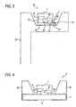
- Fig. 2 shows a flip chip type LED 2 using the light-emitting element 1.
- the LED 2 generally includes the light-emitting element 1, lead frames 30 and 31, a sub-mount board 50 as a support, and a sealing resin 35.
- Amode of mounting of the light-emitting element 1 will be described below with reference to an enlarged view (Fig. 3) of the neighborhood of a cup-like portion 33 in the lead frame 30.
- the light-emitting element 1 is mounted on the cup-like portion 33 of the lead frame 30 with interposition of the sub-mount board 50.
- the board 50 has a p-type region 51, and an n-type region 52.
- An electrically insulating film 60 of SiO 2 is formed on a surface of the board 50 except portions on which Au bumps 40 are formed.
- the p-side electrode film 20 is connected to the p-type region 51 of the board 50 through one of the Au bumps while the n-side electrode film 21 is likewise connected to the n-type region 52 of the board 50 through the other Au bump.
- the p-electrode 18 and the n-electrode 19 of the light-emitting element 1 are electrically connected to the p-type region 51 and the n-type region 52 of the board 50 respectively while the light-emitting element 1 is fixed to the board 50.
- the board 50 is bonded and fixed to the cup-like portion 33 of the lead frame 30 by silver paste 61 while a surface of the board 50 opposite to the surface on which the light-emitting element 1 is mounted is used as an adhesive surface.
- Fig. 4 shows another type light-emitting device (LED 3) formed by using the light-emitting element 1.
- the LED 3 is an SMD (Surface Mount Device) type LED. Incidentally, parts the same as those in the LED 2 are denoted by the same reference numerals.
- the LED 3 includes the light-emitting element 1, a board 70 as a support, and a reflecting member 80.
- the light-emitting element 1 is mounted on the board 70 while the electrode side of the light-emitting element 1 is used as a mount surface in the same manner as in the LED 2.
- Wiring patterns 71 are formed on surfaces of the board 70.
- the reflecting member 80 is disposed on the board 70 so that the light-emitting element 1 is surrounded by the reflecting member 80.
- the reflecting member 80 is made of a white resin, so that a surface of the reflecting member 80 can highly efficiently reflect light radiated from the light-emitting element 1.
Landscapes
- Led Devices (AREA)
- Led Device Packages (AREA)
Abstract
In a flip chip type Group III nitride compound
semiconductor light-emitting element, an Au layer is provided
on each of a surface of a p-side electrode and a surface of
an n-side electrode with interposition of a Ti layer.
Description
The present invention relates to a Group III nitride
compound semiconductor light-emitting element. Particularly
it relates to a Group III nitride compound semiconductor
light-emitting element having a p-side electrode and an n-side
electrode formed on one surface side and preferably used in
a flip chip type light-emitting device.
There is known a (flip chip type) light-emitting device
configured so that an element having a light-emitting layer
of Group III nitride compound semiconductor is mounted on a
support while a surface of the element on which a p-side electrode
and an n-side electrode are formed is used as a mount surface.
In this type light-emitting device, light emitted from the
light-emitting layer of the light-emitting element passes
through a light-transmissive substrate so as to be radiated
to the outside. The electrodes of the light-emitting element
are electrically connected to electrodes (an n layer and a p
layer or wiring patterns) of the support through electrically
conductive adhesive members respectively. High electric
conductivity is required of the electrically conductive
adhesive members. Generally, adhesive members of Au (Aubumps)
are used as the electrically conductive adhesive members. Al,
V, etc. can be used as the n-side electrode of the light-emitting
element. On the other hand, Rh, etc. low in contact resistance
and high in reflection efficiency can be used as the p-side
electrode.
When Rh is used as the p-side electrode, adhesion of Rh
to the Au bump is low. Therefore, a thick film of Au may be
formed on a surface of the p-side electrode in advance to enhance
adhesion of the p-side electrode to the Au bump. As a result,
bonding strength between the light-emitting element and the
support can be enhanced. When attention is paid to the n-side
electrode, the surface of the n-side electrode is however made
of Al etc. which is the material of the electrode. It cannot
be said that bonding strength between the n-side electrode and
the Au bump is sufficient. For this reason, there is still
room for improvement in preservative characteristic or
durability. There is also fear that a sufficient element
function cannot be exhibited because failure occurs in bonding
between the n-side electrode and the support. Furthermore,
it is undesirable from the point of view of corrosion resistance
that Al etc. which is the material of the electrode is exposed
at the surface of the n-side electrode. When the electrodes
one of which is made of Al while the other is made of Au have
to be soldered, there is a further problem in solderability
of the electrodes.
The invention is developed in consideration of the
aforementioned problems and an object of the invention is to
provide a Group III nitride compound semiconductor
light-emitting element which is excellent in preservative
characteristic or durability and which has a more stable element
function.
To achieve the foregoing object, the invention is
configured as follows. That is, according to the invention,
there is provided a Group III nitride compound semiconductor
light-emitting element having a p-side electrode and an n-side
electrode formed on one surface side, the Group III nitride
compound semiconductor light-emitting element further having:
a p-side electrode film containing Au and formed on a surface
of the p-side electrode; and an n-side electrode film containing
Au and formed on a surface of the n-side electrode.
In the aforementioned configuration, a film containing
a material (Au) of an adhesive member (Au bump) used for mounting
the light-emitting element on a support is formed on each of
a surface of the p-side electrode and a surface of the n-side
electrode to improve adhesion between each of the two electrode
surfaces and the adhesive member. As a result, when the
light-emitting element is mounted on the support, bonding
strength between the light-emitting element and the support
is improved. Accordingly, stabilization of the element
function is attained and preservative characteristic or
durability is improved.
Furthermore, because a film containing Au is formed on
each of the two electrode surfaces, corrosion resistance of
each of the two electrode surfaces is improved. It can be said
from this point of view that a Group III nitride compound
semiconductor light-emitting element high in.preservative
stability or durability is provided.
As described above, in accordance with the configuration
of the invention, a light-emitting element excellent in
preservative characteristic or durability and having a more
stable element function is provided.
Incidentally, in the aforementioned configuration,
because films the same in configuration are formed on the two
electrode surfaces, the color tones of the two electrode surfaces
can be matched with each other. Accordingly, there is also
provided an effect of attaining improvement in appearance
recognition of a surface of the light-emitting element on which
the two electrodes are formed, improvement in mount accuracy
at the time of mounting the support on the light-emitting element
having the surface used as a mount surface, improvement in
efficiency in the mounting process, etc.
A Group III nitride compound semiconductor
light-emitting element according to the invention is a flip
chip type light-emitting element having a p-side electrode and
an n-side electrode formed on one surface side. The flip chip
type light-emitting element means a light-emitting element used
in a flip chip type light-emitting device, that is, a
light-emitting element which is used to be mounted on a support
such as a board while the surface of the light-emitting element
on which the p-side electrode and the n-side electrode are formed
is used as a mount surface. Emitted light is radiated from
the board side, that is, from a side opposite to the surface
side on which the electrodes are formed.
The Group III nitride compound semiconductor
light-emitting element means a light-emitting element having
a light-emitting layer made of Group III nitride compound
semiconductor. Here, the Group III nitride compound
semiconductor is represented by the general formula
AlXGaYIn1-X-YN (0≤X≤1, 0≤Y≤1, 0≤X+Y≤1) which expresses quaternary
compounds but includes so-called binary compounds such as AlN,
GaN and InN, and so-called ternary compounds such as AlxGa1-xN,
AlxIn1-xN and GaxIn1-xN (0<x<1 in the above). The Group III
elements may be partially replaced by boron (B), thallium (Tl),
etc. The nitrogen (N) may be partially replaced by phosphorus
(P) , arsenic (As), antimony (Sb) , bismuth (Bi), etc. The Group
III nitride compound semiconductor layer may contain any
optional dopant. Si, Ge, Se, Te, C, etc. may be used as n-type
impurities. Mg, Zn, Be, Ca, Sr, Ba, etc. may be used as p-type
impurities.
The Group III nitride compound semiconductor layer can
be formed by a known method such as a metal organic chemical
vapordepositionmethod (MOCVDmethod), amolecularbeamepitaxy
method (MBE method) , a halide vapor phase epitaxy method (HVPE
method) , a sputtering method, anion-platingmethod, an electron
showering method, etc.
Incidentally, after doped with p-type impurities, the
Group III nitride compound semiconductor may be subjected to
electron beam irradiation, plasma irradiation or heating due
to a furnace. This is however not essential.
Respective members of the invention will be described
below in more detail.
A metal such as Rh, Au, Pt, Ag, Cu, Al, Ni, Co, Mg, Pd,
V, Mn, Bi, Sn, Re, etc. or its alloy can be used as a material
of the p-side electrode. Especially, Rh or Pt can be used as
a preferred material of the p-side electrode because it has
high reflection efficiency to the wavelength of light emitted
from the Group III nitride compound semiconductor
light-emitting element. The p-side electrode may be formed
as a two-layerormulti-layer structure inwhich layers different
in composition are laminated.
A p-side electrode film containing Au (gold) is formed
on a surface of the p-side electrode. The p-side electrode
film enhances adhesion of the p-side electrode to an adhesive
member of Au (hereinafter referred to as "Au bump") used at
the time of mounting the light-emitting element on the support
to consequently enhance bonding strength between the
light-emitting element and the support.
The p-side electrode film may be formed in any manner
if at least one part of the surface of the p-side electrode
can be covered with the p-side electrode film. Preferably,
the p-side electrode film is formed so that the surface of the
p-side electrode is entirely covered with the p-side electrode
film. As a result, the surface of the p-side electrode is
entirely covered with the film containing Au so that corrosion
resistance of the surface of the p-side electrode is improved.
In addition, improvement in adhesion to the Au bump can be
expected.
The p-side electrode film is preferably formed as a
laminate of a plurality of layers. For example, a two-layer
structure having a starting layer made of a metal selected from
the group consisting of Ti, Cr, W, Mo, Ta, Zr and V or an alloy
of the metal, and an upper layer made of Au or an Au alloy and
formed on the starting layer is preferably used as the p-side
electrode film. The starting layer mentioned here is used for
enhancing adhesion between the p-side electrode surface and
the upper layer (the layer made of Au or an Au alloy).
Particularly preferably, Ti, Cr or V is used as the material
of the starting layer because the starting layer can be formed
easily by vapor deposition or the like. The material of the
upper layer is preferably selected to be the same as the material
of the Au bump. This is for enhancing adhesion between the
two. Another layer may be formed between the starting layer
and the upper layer or on the upper layer.
The film thickness of the starting layer is preferably
selected to be smaller than the film thickness of the upper
layer. In other words, it is preferable that a thin starting
layer is formed on the surface of the p-side electrode and that
a thick-film upper layer is formed on the thin starting layer.
The formation of the thin starting layer suppresses increase
in electric resistance due to the starting layer. The formation
of the thick upper layer improves adhesion between the p-side
electrode film and the Au bump. The film thickness of the
starting layer is, for example, in a range of from 1 nm to 100
nm, preferably in a range of from 5 nm to 50 nm. The film thickness
of the upper layer is, for example, in a range of from 0.1 µm
to 50 µm, preferably in a range of from 0.3 µm to 3 µm.
A metal such as Al, V, Sn, Ti, Cr, Nb, Ta, Mo, W, Hf,
etc. or its alloy canbe used as amaterial of the n-side electrode.
The n-side electrode may be formed as a two-layer or multi-layer
structure in which layers different in composition are laminated.
For example, the n-side electrode may be formed as a two-layer
structure of V and Al.
An n-side electrode film containing Au (gold) is formed
on a surface of the n-side electrode, like the p-side electrode
surface.' The formation of the n-side electrode film enhances
adhesion (close contact) between the n-side electrode and the
Au bump at the time of mounting the light-emitting element on
the support by the Au bump to consequently improve bonding
strength between the light-emitting element and the support.
The n-side electrode film may be formed in any manner
if at least one part of the surface of the n-side electrode
can be covered with the n-side electrode film. Preferably,
the n-side electrode film is formed so that the surface of the
n-side electrode is entirely covered with the n-side electrode
film. As a result, the surface of the n-side electrode is
entirely covered with the film containing Au so that corrosion
resistance of the n-side electrode is improved. In addition,
improvement in adhesion to the Au bump can be expected.
The n-side electrode film is preferably formed as a
laminate of a plurality of layers. For example, a two-layer
structure having a starting layer made of a metal selected from
the group consisting of Ti, Cr, W, Mo, Ta, Zr and V or an alloy
of the metal, and an upper layer made of Au or an Au alloy and
formed on the starting layer is preferably used as the n-side
electrode film. The starting layer mentioned here is used for
enhancing adhesion between the n-side electrode surface and
the upper layer (the layer made of Au or an Au alloy).
Particularly preferably, Ti, Cr or V is used as the material
of the starting layer because the starting layer can be formed
easily by vapor deposition or the like. The material of the
upper layer is preferably selected to be the same as the material
of the Au bump. This is for enhancing adhesion between the
two. Another layer may be formed between the starting layer
and the upper layer or on the upper layer.
The film thickness of the starting layer is preferably
selected to be smaller than the film thickness of the upper
layer. In other words, it is preferable that a thin starting
layer is formed on the surface of the n-side electrode and that
a thick-film upper layer is formed on the thin starting layer.
The formation of the thin starting layer suppresses increase
in electric resistance due to the starting layer. The formation
of the thick upper layer improves adhesion between the n-side
electrode film and the Au bump. The film thickness of the
starting layer is, for example, in a range of from 1 nm to 100
nm, preferably in a range of from 5 nm to 50 nm. The film thickness
of the upper layer is, for example, in a range of from 0.1 µm
to 50 µm, preferably in a range of from 0.3 µm to 3 µm.
The configuration of the n-side electrode film is
preferably selected to the same as the configuration of the
p-side electrode film. In such a mode, the n-side electrode
film and the p-side electrode film can be formed simultaneously,
so that the production process can be simplified. For example,
each of the n-side electrode film and the p-side electrode film
is formed as a structure having a starting layer of Ti, and
an upper layer of Au laminated on the starting layer.
For example, the Group III nitride compound semiconductor
element light-emitting element according to the invention can
be produced as follows.
First, a substrate on which Group III nitride compound
semiconductor layers can be grown is prepared. A plurality
of semiconductor layers are laminated on the substrate so that
at least an n-type Group III nitride compound semiconductor
layer, a light-emitting layer of Group III nitride compound
semiconductor and a p-type Group III nitride compound
semiconductor layer are arranged in order. Sapphire, spinel,
silicon, silicon carbide, zinc oxide, gallium phosphide,
gallium arsenide, magnesium oxide, manganese oxide, Group III
nitride compound semiconductor single crystal, etc. can be used
as the substrate. When a sapphire substrate is used, a face
a of the substrate is preferably used.
Then, an etching process is applied to reveal a part of
the n-type semiconductor layer. Then, a p-side electrode and
an n-side electrode are formed on the p-type Group III nitride
compound semiconductor layer and on the n-type Group III nitride
compound semiconductor layer respectively. The p-side
electrode and the n-side electrode can be formed by a known
method such as vapor deposition, sputtering, etc. Then, a
surface of the sample is cleaned. Examples of the cleaning
method include heating, ultraviolet-ray irradiation, etc.
When the sample surface, especially a surface of the n-electrode
is cleaned, sufficient bonding strength can be kept between
the n-side electrode and an n-side electrode film. Then, a
p-side electrode film is formed on a surface of the p-side
electrode. Similarly, an n-side electrode film is formed on
a surface of the n-side electrode. Each of the p-side electrode
film and the n-side electrode film can be formed by a known
method such as vapor deposition, sputtering, etc. When the
p-side electrode film and the n-side electrode are selected
to be equal in configuration to each other, the p-side electrode
film and the n-side electrode film can be formed simultaneously.
The configuration of the invention will be described below
in more detail in connection with an embodiment of the invention.
Fig. 1 is a view typically showing the configuration of
a light-emitting element 1 as an embodiment. Specifications
of respective layers in the light-emitting element 1 are as
follows.
| Layer | Composition |
| p-type layer 15 | p-GaN: |
| Layer | |
| 14 containing a light-emitting layer | inclusive of InGaN layer |
| n-type layer 13 | n-GaN: |
| Buffer layer | |
| 12 | |
| Substrate | |
| 11 | sapphire |
Ann-type layer 13 of GaNdopedwith Si as n-type impurities
is formed on a substrate 11 with interposition of a buffer layer
12. Although sapphire is used as the substrate 11 here, the
substrate 11 is not limited thereto. Sapphire, spinel, silicon,
silicon carbide, zinc oxide, gallium phosphide, gallium
arsenide, magnesium oxide, manganese oxide, Group III nitride
compound semiconductor single crystal, etc. may be used.
Although the buffer layer is made of AlN by an MOCVD method,
the buffer layer is not limited thereto. GaN, InN, AlGaN, InGaN,
AlInGaN, etc. may be used as the material of the buffer layer.
A molecular beam epitaxy method (MBE method), a halide vapor
phase epitaxy method (HVPE method), a sputtering method, an
ion-plating method, an electron showering method, etc. may be
used as the method for producing the buffer layer. When Group
III nitride compound semiconductor is used as the substrate,
the buffer layer can be omitted.
Furthermore, after the semiconductor element is formed,
the substrate and the buffer layer may be removed as occasion
demands.
Although the n-type layer is made of GaN here, AlGaN,
InGaN or AlInGaN may be used.
Although the n-type layer is doped with Si as n-type
impurities, other n-type impurities such as Ge, Se, Te, C, etc.
may be used.
The n-type layer 13 may be of a two-layer structure having
an n- layer of low electron density on the light-emitting
layer-containing layer 14 side, and an n+ layer of high electron
density on the buffer layer 12 side.
The layer 14 containing a light-emitting layer may contain
a light-emitting layer of a quantum well structure. A single
hetero type structure, a double hetero type structure, a
homo-junction type structure, etc. maybe used as the structure
of the light-emitting element.
The layer 14 containing a light-emitting layer may contain
a Group III nitride compound semiconductor layer doped with
an acceptor such as magnesium etc. and formed on the p-type
layer 15 side so as to have a wide band gap. This is provided
for effectively preventing electrons injected into the layer
14 containing a light-emitting layer from diffusing into the
p-type layer 15.
Ap-type layer 15 of GaN doped with Mg as p-type impurities
is formed on the layer 14 containing a light-emitting layer.
The p-type layer may be made of AlGaN, InGaN or InAlGaN. Zn,
Be, Ca, Sr or Ba may be used as p-type impurities.
The p-type layer 15 may be of a two-layer structure having
a p- layer of low hole density on the layer 14 containing a
light-emitting layer side, and a p+ layer of high hole density
on the electrode side.
In the light-emitting diode configured as described above,
each Group III nitride compound semiconductor layermaybe formed
by MOCVD executed in a general condition or may be formed by
a method such as a molecular beam epitaxy method (MBE method) ,
a halide vapor phase epitaxy method (HVPE method), a sputtering
method, an ion-plating method, an electron showering method,
etc.
After the p-type layer 15 is formed, the p-type layer
15, the layer 14 containing a light-emitting layer and the n-type
layer 13 are partially removed by etching to reveal a part of
the n-type layer 13.
Then, a p-electrode 18 of Rh is formed on the p-type layer
15 by vapor deposition. An n-electrode 19, which is composed
of two layers of Al and V, is formed on the n-type layer 13
by vapor deposition. Then, alloying is performed by known
means.
Each of a p-side electrode film 20 and an n-side electrode
film 21 is composed of a starting layer 20a or 21a of Ti, and
an upper layer 20b or 21b of Au laminated on the starting layer
20a or 21a. Each of the p-side electrode film 20 and the n-side
electrode film 21 is formed by a lift-off method. In this
embodiment, the film thickness of each of the starting layers
20a and 21a is set at 10 nm, and the film thickness of each
of the upper layers 20b and 21b is set at 1 µm.
After the aforementionedprocess, aprocess of separation
into chips is carried out by using a scriber or the like.
Next, an example of a light-emitting device formed by
using the light-emitting element 1 will be described. Fig.
2 shows a flip chip type LED 2 using the light-emitting element
1. The LED 2 generally includes the light-emitting element
1, lead frames 30 and 31, a sub-mount board 50 as a support,
and a sealing resin 35. Amode of mounting of the light-emitting
element 1 will be described below with reference to an enlarged
view (Fig. 3) of the neighborhood of a cup-like portion 33 in
the lead frame 30.
The light-emitting element 1 is mounted on the cup-like
portion 33 of the lead frame 30 with interposition of the
sub-mount board 50. The board 50 has a p-type region 51, and
an n-type region 52. An electrically insulating film 60 of
SiO2 is formed on a surface of the board 50 except portions
on which Au bumps 40 are formed. As shown in the drawing, when
the light-emitting element 1 having its electrode side face
downward is sub-mounted on the board 50, the p-side electrode
film 20 is connected to the p-type region 51 of the board 50
through one of the Au bumps while the n-side electrode film
21 is likewise connected to the n-type region 52 of the board
50 through the other Au bump. As a result, the p-electrode
18 and the n-electrode 19 of the light-emitting element 1 are
electrically connected to the p-type region 51 and the n-type
region 52 of the board 50 respectively while the light-emitting
element 1 is fixed to the board 50. The board 50 is bonded
and fixed to the cup-like portion 33 of the lead frame 30 by
silver paste 61 while a surface of the board 50 opposite to
the surface on which the light-emitting element 1 is mounted
is used as an adhesive surface.
Fig. 4 shows another type light-emitting device (LED 3)
formed by using the light-emitting element 1. The LED 3 is
an SMD (Surface Mount Device) type LED. Incidentally, parts
the same as those in the LED 2 are denoted by the same reference
numerals.
The LED 3 includes the light-emitting element 1, a board
70 as a support, and a reflecting member 80. The light-emitting
element 1 is mounted on the board 70 while the electrode side
of the light-emitting element 1 is used as a mount surface in
the same manner as in the LED 2. Wiring patterns 71 are formed
on surfaces of the board 70. When the p-side electrode film
20 and the n-side electrode film 21 of the light-emitting element
1 are bonded to the wiring patterns through the Au bumps 40,
the two electrodes of the light-emitting element 1 are
electrically connected to the wiring patterns. The reflecting
member 80 is disposed on the board 70 so that the light-emitting
element 1 is surrounded by the reflecting member 80. The
reflecting member 80 is made of a white resin, so that a surface
of the reflecting member 80 can highly efficiently reflect light
radiated from the light-emitting element 1.
Although the invention has been described in detail and
with reference to a specific embodiment, it is obvious to those
skilled in the art that various changes or modifications may
be made without departing from the spirit and scope of the
invention.
This application is based on Japanese Patent Application
(Japanese Patent Application No. 2001-170908) filed on June
6, 2001. The contents thereof must be incorporated herein by
reference.
The invention is not limited to the description of mode
for carrying out the invention at all. Various modifications
that can be easily conceived by those skilled in the art are
also included in the invention without departing from the scope
of Claim.
The following items are disclosed.
- 21. A method of producing a flip chip type Group III nitride
compound semiconductor light-emitting element having a p-side
electrode and an n-side electrode formed on one surface side,
including the steps of:
- forming ap-side electrode film containing Au on the p-side electrode; and
- forming an n-side electrode film containing Au on the n-side electrode.
Claims (19)
- A Group III nitride compound semiconductor light-emitting element having a p-side electrode and an n-side electrode formed on one surface side, said Group III nitride compound semiconductor light-emitting element further having:a p-side electrode film containing Au and formed on a surface of said p-side electrode; andan n-side electrode film containing Au and formed on a surface of said n-side electrode.
- A Group III nitride compound semiconductor light-emitting element according to claim 1, wherein saidp-side electrode film is composed of a plurality of layers including a starting layer, and an upper layer formed on said starting layer, said starting layer being made of a metal selected from the group consisting of Ti, Cr, W, Mo, Ta, Zr and V or an alloy of said metal, said upper layer being made of Au or an Au alloy.
- A Group III nitride compound semiconductor light-emitting element according to claim 2, wherein said starting layer is made of Ti or a Ti alloy.
- A Group III nitride compound semiconductor light-emitting element according to claim 1, wherein saidn-side electrode film is composed of a plurality of layers including a starting layer, and an upper layer formed on said starting layer, said starting layer being made of a metal selected from the group consisting of Ti, Cr, W, Mo, Ta, Zr and V or an alloy of said metal, said upper layer being made of Au or an Au alloy.
- A Group III nitride compound semiconductor light-emitting element according to claim 4, wherein said starting layer is made of Ti or a Ti alloy.
- A Group III nitride compound semiconductor light-emitting element according to claim 1, wherein saidp-side electrode film and said n-side electrode film are the same in layer structure.
- A Group III nitride compound semiconductor light-emitting element according to claim 1, wherein saidp-side electrode film is formed so that a surface of said p-side electrode is entirely covered with said p-side electrode film.
- A Group III nitride compound semiconductor light-emitting element according to claim 1, wherein said n-side electrode film is formed so that a surface of said n-side electrode is entirely covered with said n-side electrode film.
- A light-emitting device comprising:a Group III nitride compound semiconductor light-emitting element having a p-side electrode and an n-side electrode formed on one surface side and further having a p-side electrode film containing Au and formed on a surface of said p-side electrode, and an n-side electrode film containing Au and formed on a surface of said n-side electrode; anda support on which said light-emitting element is mounted.
- A light-emitting device according to claim 9, wherein said light-emitting element is mounted on said support through Au bumps.
- A light-emitting device according to claim 9, wherein said support is a board having a p-side region connected to said p-side electrode, and an n-side region connected to said n-side electrode.
- A light-emitting device according to claim 9, wherein said support is a board having wiring patterns connected to said p-side electrode and said n-side electrode.
- A light-emitting device according to claim 9, wherein said p-side electrode film is composed of a plurality of layers including a starting layer, and an upper layer formed on said starting layer, said starting layer being made of a metal selected from the group consisting of Ti, Cr, W, Mo, Ta, Zr and V or an alloy of said metal, said upper layer being made of Au or an Au alloy.
- A Group III nitride compound semiconductor light-emitting device according to claim 13, wherein said starting layer is made of Ti or a Ti alloy.
- A light-emitting device according to claim 9, wherein said n-side electrode film is composed of a plurality of layers including a starting layer, and an upper layer formed on said starting layer, said starting layer being made of a metal selected from the group consisting of Ti, Cr, W, Mo, Ta, Zr and V or an alloy of said metal, said upper layer being made of Au or an Au alloy.
- A light-emitting device according to claim 15, wherein said starting layer is made of Ti or a Ti alloy.
- A light-emitting device according to claim 9, wherein said p-side electrode film and said n-side electrode film are the same in layer structure.
- A light-emitting device according to claim 9, wherein said p-side electrode film is formed so that a surface of said p-side electrode is entirely covered with said p-side electrode film.
- A light-emitting device according to claim 9, wherein said n-side electrode film is formed so that a surface of said n-side electrode is entirely covered with said n-side electrode film.
Applications Claiming Priority (3)
| Application Number | Priority Date | Filing Date | Title |
|---|---|---|---|
| JP2001170908A JP3912044B2 (en) | 2001-06-06 | 2001-06-06 | Method for manufacturing group III nitride compound semiconductor light emitting device |
| JP2001170908 | 2001-06-06 | ||
| PCT/JP2002/005430 WO2002101841A1 (en) | 2001-06-06 | 2002-06-03 | Iii group nitride based semiconductor luminescent element |
Publications (2)
| Publication Number | Publication Date |
|---|---|
| EP1406313A1 true EP1406313A1 (en) | 2004-04-07 |
| EP1406313A4 EP1406313A4 (en) | 2006-01-11 |
Family
ID=19012758
Family Applications (1)
| Application Number | Title | Priority Date | Filing Date |
|---|---|---|---|
| EP02730876A Withdrawn EP1406313A4 (en) | 2001-06-06 | 2002-06-03 | LUMINESCENT SEMICONDUCTOR ELEMENT BASED ON GROUP III NITRIDE |
Country Status (7)
| Country | Link |
|---|---|
| US (1) | US7005684B2 (en) |
| EP (1) | EP1406313A4 (en) |
| JP (1) | JP3912044B2 (en) |
| KR (1) | KR100594534B1 (en) |
| CN (1) | CN1309099C (en) |
| TW (1) | TW546856B (en) |
| WO (1) | WO2002101841A1 (en) |
Cited By (3)
| Publication number | Priority date | Publication date | Assignee | Title |
|---|---|---|---|---|
| WO2004010509A3 (en) * | 2002-07-22 | 2004-09-23 | Cree Inc | Light emitting diode including barrier layers and manufacturing methods therefor |
| EP2320484A1 (en) * | 2001-07-23 | 2011-05-11 | Cree, Inc. | Light emitting diode including barrier layers and manufacturing method therefore |
| US8269241B2 (en) | 2001-07-23 | 2012-09-18 | Cree, Inc. | Light emitting diodes including barrier layers/sublayers and manufacturing methods therefor |
Families Citing this family (35)
| Publication number | Priority date | Publication date | Assignee | Title |
|---|---|---|---|---|
| US6791119B2 (en) | 2001-02-01 | 2004-09-14 | Cree, Inc. | Light emitting diodes including modifications for light extraction |
| US20030090103A1 (en) * | 2001-11-09 | 2003-05-15 | Thomas Becker | Direct mailing device |
| DE10203809B4 (en) * | 2002-01-31 | 2010-05-27 | Osram Opto Semiconductors Gmbh | Radiation-emitting semiconductor component |
| JP4030534B2 (en) * | 2003-07-25 | 2008-01-09 | 昭和電工株式会社 | Compound semiconductor light emitting device and manufacturing method thereof |
| WO2005022654A2 (en) * | 2003-08-28 | 2005-03-10 | Matsushita Electric Industrial Co.,Ltd. | Semiconductor light emitting device, light emitting module, lighting apparatus, display element and manufacturing method of semiconductor light emitting device |
| KR100571816B1 (en) * | 2003-09-08 | 2006-04-17 | 삼성전자주식회사 | Nitride-based light emitting device and its manufacturing method |
| JP2005142545A (en) * | 2003-10-14 | 2005-06-02 | Showa Denko Kk | Gallium nitride compound semiconductor light emitting device, positive electrode thereof, light emitting diode using the same, and lamp using the same |
| TWI264833B (en) * | 2003-10-14 | 2006-10-21 | Showa Denko Kk | Gallium nitride-based compound semiconductor light-emitting device, positive electrode for the device, light-emitting diode and lamp using the device |
| TW200520240A (en) * | 2003-10-14 | 2005-06-16 | Showa Denko Kk | Gallium nitride-based compound semiconductor light-emitting device, positive electrode for the device, light-emitting diode and lamp using the device |
| JP2005142544A (en) * | 2003-10-14 | 2005-06-02 | Showa Denko Kk | Gallium nitride-based compound semiconductor light emitting element, its positive electrode, light emitting diode using it, and lamp using it |
| WO2005057642A1 (en) * | 2003-12-10 | 2005-06-23 | Showa Denko K.K. | Gallium nitride-based compound semiconductor light-emitting device and negative electrode thereof |
| US7518163B2 (en) | 2003-12-17 | 2009-04-14 | Showa Denko K.K. | Gallium nitride-based compound semiconductor light-emitting device and negative electrode thereof |
| KR100586948B1 (en) * | 2004-01-19 | 2006-06-07 | 삼성전기주식회사 | Nitride semiconductor light emitting device and manufacturing method |
| JP2005268275A (en) * | 2004-03-16 | 2005-09-29 | Sanyo Electric Co Ltd | Nitride based semiconductor light emitting diode element |
| US7417220B2 (en) * | 2004-09-09 | 2008-08-26 | Toyoda Gosei Co., Ltd. | Solid state device and light-emitting element |
| CN100353576C (en) * | 2004-11-19 | 2007-12-05 | 中国科学院半导体研究所 | Production of inverted gallium nitride base light emitting diode chip |
| JP2006156747A (en) * | 2004-11-30 | 2006-06-15 | Ngk Spark Plug Co Ltd | Wiring board |
| US20060124941A1 (en) * | 2004-12-13 | 2006-06-15 | Lee Jae S | Thin gallium nitride light emitting diode device |
| KR100631898B1 (en) * | 2005-01-19 | 2006-10-11 | 삼성전기주식회사 | Gallium nitride based light emitting device having ESD protection capability and method for manufacturing same |
| KR100675220B1 (en) * | 2005-05-18 | 2007-01-29 | 삼성전기주식회사 | Nitride semiconductor light emitting device |
| JP5138873B2 (en) | 2005-05-19 | 2013-02-06 | 日亜化学工業株式会社 | Nitride semiconductor device |
| JP2007158131A (en) * | 2005-12-06 | 2007-06-21 | Toyoda Gosei Co Ltd | Group III nitride compound semiconductor optical device |
| US7772604B2 (en) | 2006-01-05 | 2010-08-10 | Illumitex | Separate optical device for directing light from an LED |
| US9406505B2 (en) | 2006-02-23 | 2016-08-02 | Allos Semiconductors Gmbh | Nitride semiconductor component and process for its production |
| WO2008042351A2 (en) | 2006-10-02 | 2008-04-10 | Illumitex, Inc. | Led system and method |
| US20090275266A1 (en) * | 2006-10-02 | 2009-11-05 | Illumitex, Inc. | Optical device polishing |
| JP2011512037A (en) * | 2008-02-08 | 2011-04-14 | イルミテックス, インコーポレイテッド | System and method for emitter layer shaping |
| TW201034256A (en) * | 2008-12-11 | 2010-09-16 | Illumitex Inc | Systems and methods for packaging light-emitting diode devices |
| US8449128B2 (en) * | 2009-08-20 | 2013-05-28 | Illumitex, Inc. | System and method for a lens and phosphor layer |
| US8585253B2 (en) | 2009-08-20 | 2013-11-19 | Illumitex, Inc. | System and method for color mixing lens array |
| EP2628192B1 (en) * | 2010-10-12 | 2018-08-08 | Lumileds Holding B.V. | Light emitting device with reduced epi stress |
| KR20130024089A (en) * | 2011-08-30 | 2013-03-08 | 엘지이노텍 주식회사 | Light emitting device |
| KR102042258B1 (en) * | 2013-01-29 | 2019-11-07 | 엘지이노텍 주식회사 | Light emitting device |
| KR102075147B1 (en) * | 2013-06-05 | 2020-02-10 | 엘지이노텍 주식회사 | Light emitting device and light emitting device package |
| JP6698231B2 (en) * | 2018-02-01 | 2020-05-27 | パナソニック株式会社 | Semiconductor device and method of manufacturing semiconductor device |
Family Cites Families (27)
| Publication number | Priority date | Publication date | Assignee | Title |
|---|---|---|---|---|
| JP2704181B2 (en) * | 1989-02-13 | 1998-01-26 | 日本電信電話株式会社 | Method for growing compound semiconductor single crystal thin film |
| JPH03183173A (en) | 1989-12-13 | 1991-08-09 | Canon Inc | optical element |
| JP2666228B2 (en) | 1991-10-30 | 1997-10-22 | 豊田合成株式会社 | Gallium nitride based compound semiconductor light emitting device |
| EP0952617B1 (en) * | 1993-04-28 | 2004-07-28 | Nichia Corporation | Gallium nitride-based III-V group compound semiconductor device |
| US5889295A (en) * | 1996-02-26 | 1999-03-30 | Kabushiki Kaisha Toshiba | Semiconductor device |
| US6121127A (en) * | 1996-06-14 | 2000-09-19 | Toyoda Gosei Co., Ltd. | Methods and devices related to electrodes for p-type group III nitride compound semiconductors |
| JPH10125655A (en) * | 1996-10-23 | 1998-05-15 | Sony Corp | Manufacture of iii-v compound semiconductor element |
| JP3737226B2 (en) * | 1996-12-24 | 2006-01-18 | ローム株式会社 | Semiconductor light emitting device |
| EP2264794B1 (en) * | 1997-01-09 | 2014-11-19 | Nichia Corporation | Nitride semiconductor device |
| US6333522B1 (en) * | 1997-01-31 | 2001-12-25 | Matsushita Electric Industrial Co., Ltd. | Light-emitting element, semiconductor light-emitting device, and manufacturing methods therefor |
| JPH10247747A (en) * | 1997-03-05 | 1998-09-14 | Toshiba Corp | Semiconductor light emitting device and method of manufacturing the same |
| US6268618B1 (en) * | 1997-05-08 | 2001-07-31 | Showa Denko K.K. | Electrode for light-emitting semiconductor devices and method of producing the electrode |
| JP4119501B2 (en) * | 1997-07-10 | 2008-07-16 | ローム株式会社 | Semiconductor light emitting device |
| JP3462720B2 (en) * | 1997-07-16 | 2003-11-05 | 三洋電機株式会社 | N-type nitride semiconductor electrode, semiconductor element having the electrode, and method of manufacturing the same |
| JP3965610B2 (en) * | 1997-08-01 | 2007-08-29 | 富士通株式会社 | Semiconductor device and manufacturing method thereof |
| JP3457516B2 (en) * | 1997-08-27 | 2003-10-20 | 株式会社東芝 | Gallium nitride based compound semiconductor device |
| JP3822976B2 (en) * | 1998-03-06 | 2006-09-20 | ソニー株式会社 | Semiconductor device and manufacturing method thereof |
| JP4183299B2 (en) * | 1998-03-25 | 2008-11-19 | 株式会社東芝 | Gallium nitride compound semiconductor light emitting device |
| JP3625377B2 (en) * | 1998-05-25 | 2005-03-02 | ローム株式会社 | Semiconductor light emitting device |
| JP4352473B2 (en) * | 1998-06-26 | 2009-10-28 | ソニー株式会社 | Manufacturing method of semiconductor device |
| JP3739951B2 (en) | 1998-11-25 | 2006-01-25 | 東芝電子エンジニアリング株式会社 | Semiconductor light emitting device and manufacturing method thereof |
| JP2000252230A (en) * | 1998-12-28 | 2000-09-14 | Sanyo Electric Co Ltd | Semiconductor device and method of manufacturing the same |
| JP4296644B2 (en) * | 1999-01-29 | 2009-07-15 | 豊田合成株式会社 | Light emitting diode |
| ATE452445T1 (en) * | 1999-03-04 | 2010-01-15 | Nichia Corp | NITRIDE SEMICONDUCTOR LASER ELEMENT |
| JP3881473B2 (en) | 1999-04-30 | 2007-02-14 | ローム株式会社 | Manufacturing method of semiconductor light emitting device |
| JP3833848B2 (en) * | 1999-05-10 | 2006-10-18 | パイオニア株式会社 | Group 3 nitride semiconductor device manufacturing method |
| PL202938B1 (en) * | 2000-02-16 | 2009-08-31 | Nichia Corp | Nitride semiconductor laser device |
-
2001
- 2001-06-06 JP JP2001170908A patent/JP3912044B2/en not_active Expired - Fee Related
-
2002
- 2002-06-03 KR KR1020037016010A patent/KR100594534B1/en not_active Expired - Lifetime
- 2002-06-03 US US10/479,602 patent/US7005684B2/en not_active Expired - Lifetime
- 2002-06-03 WO PCT/JP2002/005430 patent/WO2002101841A1/en not_active Ceased
- 2002-06-03 CN CNB028111990A patent/CN1309099C/en not_active Expired - Lifetime
- 2002-06-03 EP EP02730876A patent/EP1406313A4/en not_active Withdrawn
- 2002-06-05 TW TW091112090A patent/TW546856B/en not_active IP Right Cessation
Cited By (5)
| Publication number | Priority date | Publication date | Assignee | Title |
|---|---|---|---|---|
| EP2320484A1 (en) * | 2001-07-23 | 2011-05-11 | Cree, Inc. | Light emitting diode including barrier layers and manufacturing method therefore |
| US8269241B2 (en) | 2001-07-23 | 2012-09-18 | Cree, Inc. | Light emitting diodes including barrier layers/sublayers and manufacturing methods therefor |
| US8604502B2 (en) | 2001-07-23 | 2013-12-10 | Cree, Inc. | Light emitting diodes including barrier sublayers |
| US8907366B2 (en) | 2001-07-23 | 2014-12-09 | Cree, Inc. | Light emitting diodes including current spreading layer and barrier sublayers |
| WO2004010509A3 (en) * | 2002-07-22 | 2004-09-23 | Cree Inc | Light emitting diode including barrier layers and manufacturing methods therefor |
Also Published As
| Publication number | Publication date |
|---|---|
| CN1309099C (en) | 2007-04-04 |
| US20040149999A1 (en) | 2004-08-05 |
| US7005684B2 (en) | 2006-02-28 |
| KR100594534B1 (en) | 2006-06-30 |
| CN1513212A (en) | 2004-07-14 |
| JP3912044B2 (en) | 2007-05-09 |
| EP1406313A4 (en) | 2006-01-11 |
| TW546856B (en) | 2003-08-11 |
| KR20040004700A (en) | 2004-01-13 |
| JP2002368271A (en) | 2002-12-20 |
| WO2002101841A1 (en) | 2002-12-19 |
Similar Documents
| Publication | Publication Date | Title |
|---|---|---|
| US7005684B2 (en) | Group III nitride based semiconductor luminescent element | |
| KR101327106B1 (en) | Semiconductor light emitting device | |
| US7291865B2 (en) | Light-emitting semiconductor device | |
| US6794690B2 (en) | Group III nitride compound semiconductor light-emitting element | |
| US7157294B2 (en) | Group III nitride compound semiconductor light-emitting element | |
| EP2763192B1 (en) | Nitride semiconductor element and method for producing same | |
| JP5162909B2 (en) | Semiconductor light emitting device | |
| KR100573346B1 (en) | Group III nitride compound semiconductor light emitting device | |
| JP5045336B2 (en) | Semiconductor light emitting device | |
| US6593597B2 (en) | Group III-V element-based LED having ESD protection capacity | |
| US9450017B2 (en) | Semiconductor light emitting device and method of fabricating the same | |
| US20090085052A1 (en) | Gan type light emitting diode device and method of manufacturing the same | |
| KR100895452B1 (en) | Positive electrode for semiconductor light-emitting device | |
| JP4572597B2 (en) | Nitride semiconductor device | |
| US20040201110A1 (en) | Flip-chip light emitting diode with indium-tin-oxide based reflecting contacts | |
| JP2000294837A (en) | Gallium nitride based compound semiconductor light emitting device | |
| US7687821B2 (en) | Gallium nitride based light emitting diode | |
| JP2006108161A (en) | Semiconductor light emitting device | |
| US20060261358A1 (en) | Flip chip light emitting diode and method of manufacturing the same | |
| JP4868821B2 (en) | Gallium nitride compound semiconductor and light emitting device | |
| US20060097283A1 (en) | Group III-nitride-based compound semiconductor device | |
| JP2006013034A (en) | Group iii nitride compound semiconductor light-emitting device and manufacturing method therefor | |
| JP2005019919A (en) | Light emitting device | |
| JP2006120731A (en) | Nitride semiconductor light emitting device |
Legal Events
| Date | Code | Title | Description |
|---|---|---|---|
| PUAI | Public reference made under article 153(3) epc to a published international application that has entered the european phase |
Free format text: ORIGINAL CODE: 0009012 |
|
| 17P | Request for examination filed |
Effective date: 20031205 |
|
| AK | Designated contracting states |
Kind code of ref document: A1 Designated state(s): AT BE CH CY DE DK ES FI FR GB GR IE IT LI LU MC NL PT SE TR |
|
| AX | Request for extension of the european patent |
Extension state: AL LT LV MK RO SI |
|
| A4 | Supplementary search report drawn up and despatched |
Effective date: 20051124 |
|
| 17Q | First examination report despatched |
Effective date: 20070419 |
|
| STAA | Information on the status of an ep patent application or granted ep patent |
Free format text: STATUS: THE APPLICATION IS DEEMED TO BE WITHDRAWN |
|
| 18D | Application deemed to be withdrawn |
Effective date: 20100105 |