EP1406287A1 - Plasma display - Google Patents
Plasma display Download PDFInfo
- Publication number
- EP1406287A1 EP1406287A1 EP03717633A EP03717633A EP1406287A1 EP 1406287 A1 EP1406287 A1 EP 1406287A1 EP 03717633 A EP03717633 A EP 03717633A EP 03717633 A EP03717633 A EP 03717633A EP 1406287 A1 EP1406287 A1 EP 1406287A1
- Authority
- EP
- European Patent Office
- Prior art keywords
- discharge
- recess
- electrodes
- plasma display
- display device
- Prior art date
- Legal status (The legal status is an assumption and is not a legal conclusion. Google has not performed a legal analysis and makes no representation as to the accuracy of the status listed.)
- Withdrawn
Links
Images






Classifications
-
- H—ELECTRICITY
- H01—ELECTRIC ELEMENTS
- H01J—ELECTRIC DISCHARGE TUBES OR DISCHARGE LAMPS
- H01J11/00—Gas-filled discharge tubes with alternating current induction of the discharge, e.g. alternating current plasma display panels [AC-PDP]; Gas-filled discharge tubes without any main electrode inside the vessel; Gas-filled discharge tubes with at least one main electrode outside the vessel
- H01J11/20—Constructional details
- H01J11/34—Vessels, containers or parts thereof, e.g. substrates
- H01J11/38—Dielectric or insulating layers
-
- H—ELECTRICITY
- H01—ELECTRIC ELEMENTS
- H01J—ELECTRIC DISCHARGE TUBES OR DISCHARGE LAMPS
- H01J11/00—Gas-filled discharge tubes with alternating current induction of the discharge, e.g. alternating current plasma display panels [AC-PDP]; Gas-filled discharge tubes without any main electrode inside the vessel; Gas-filled discharge tubes with at least one main electrode outside the vessel
- H01J11/10—AC-PDPs with at least one main electrode being out of contact with the plasma
- H01J11/12—AC-PDPs with at least one main electrode being out of contact with the plasma with main electrodes provided on both sides of the discharge space
-
- H—ELECTRICITY
- H01—ELECTRIC ELEMENTS
- H01J—ELECTRIC DISCHARGE TUBES OR DISCHARGE LAMPS
- H01J11/00—Gas-filled discharge tubes with alternating current induction of the discharge, e.g. alternating current plasma display panels [AC-PDP]; Gas-filled discharge tubes without any main electrode inside the vessel; Gas-filled discharge tubes with at least one main electrode outside the vessel
- H01J11/20—Constructional details
- H01J11/22—Electrodes, e.g. special shape, material or configuration
- H01J11/24—Sustain electrodes or scan electrodes
-
- H—ELECTRICITY
- H01—ELECTRIC ELEMENTS
- H01J—ELECTRIC DISCHARGE TUBES OR DISCHARGE LAMPS
- H01J2211/00—Plasma display panels with alternate current induction of the discharge, e.g. AC-PDPs
- H01J2211/20—Constructional details
- H01J2211/22—Electrodes
- H01J2211/24—Sustain electrodes or scan electrodes
- H01J2211/245—Shape, e.g. cross section or pattern
Definitions
- the present invention relates to plasma display devices known as display devices.
- PDP plasma display panel
- the driving schemes of PDP can be broadly divided into AC type and DC type.
- Thebacke two types of discharge schemes namely, surface discharge type and opposing discharge type.
- AC type and surface discharge type PDP's are dominant from the standpoints of achieving higher definition and larger shield, and simplicity of manufacturing.
- Fig. 20 shows an example of a conventional PDP panel structure. As illustrated in Fig. 20, the PDP is comprised of front panel 1 and back panel 2.
- Front panel 1 is comprised of transparent front substrate 3, a plurarity of display electrodes 6, dielectric layer 7, and protective film 8.
- Front substrate 3 is a glass substrate such as made from boron silicide sodium glass fabricated by the floating method.
- Display electrodes 6 consist of a pair of scan electrode 4 and sustain electrode 5, and a plurarity of pairs are laid out on front substrate 3 in a striped manner.
- Dielectric layer 7 is formed in a manner covering a group of display electrodes 6, and protective film 8 made from MgO is formed on dielectric layer 7.
- scan electrode 4 and sustain electrode 5 consist of transparent electrodes 4a, 5a that serve as discharge electrodes and bus electrodes 4b, 5b that are electrically connected with transparent electrodes 4a, 5a, respectively.
- Bus electrodes 4b, 5b are formed with such material as Cr/Cu/Cr, Ag or the like.
- Back panel 2 consists of back substrate 9, address electrodes 10, dielectric layer 11, a plurarity of stripe-shaped barrier ribs 12, and phosphor layers 13.
- Address electrodes 10 are formed on back substrate 9 that is disposed opposite front substrate 3 in the direction orthogonal to display electrodes 6.
- Dielectric layer 11 is formed in a manner covering address electrodes 10.
- Each ribs 12 are formed on dielectric layer 11 between address electrodes 10 and in parallel to address electrodes 10.
- Phosphor layer 13 is formed on the sides between ribs 12 and on the surface of dielectric layer 11.
- phosphor layer 13 normally consists of three sequentially disposed colors of red, green, and blue.
- front and back panels 1, 2 are opposed to each other across a minute discharge space with display electrodes 6 orthogonal to address electrodes 10, and their periphery is sealed with a sealing member.
- the discharge space is filled with discharge gas, which is made by mixing for example, neon (Ne) and xenon (Xe), at a pressure of about 66,500 Pa (500 Torr). In this way, the PDP is formed.
- the discharge space of this PDP is partitioned into a plurality of sections by barrier ribs 12, and a plurality of discharge cells or light-emitting pixel regions is each defined by barrier ribs 12 and display and address electrodes 6, 10 that are orthogonal to each other.
- scan and sustain electrodes 4, 5 of display electrode 6 are disposed with discharging gap 14 between these electrodes 4, 5.
- Light-emitting pixel region 15 is a region surrounded by this display electrode 6 and barrier ribs 12, and non-light-emitting pixel region 16 is an adjoining gap or region between adjacent display electrodes 6. Also, a black stripe is sometimes formed in non-light-emitting pixel region 16 for the purpose of improving the contrast.
- the plasma display device of the present invention includes a pair of front substrate and a back substrate that are opposingly disposed in a manner such that discharge spaces partitioned by ribs are formed between the substrates, a pair of display electrodes comprising discharge electrodes that are opposingly disposed on the front substrate for each display line with discharge gaps interposed in a manner such that discharge cells are formed between the ribs and bus electrodes for supplying power to the discharge electrodes, and a dielectric layer formed in a manner covering the display electrodes, where the dielectric layer has at least one recess formed on the surface on the side of the discharge space of each discharge cell, and the discharge electrodes are formed in a manner projecting out from the bus electrodes toward the discharge gap in a manner opposing to each other in the bottom region of the recess with the discharge gap interposed.
- Fig. 1 is a sectional perspective view of an example of panel structure of a plasma display panel as used in the plasma display device in Preferred Embodiment - 1 of the present invention.
- the PDP consists of front panel 21 and back panel 22.
- Front panel 21 consists of transparent front substrate 23, a plurarity of display electrodes 26, dielectric layer 27, and protective film 28.
- Front substrate 23 is a glass substrate made of boron silicate sodium glass prepared by a float prpcess, for example.
- a plurarity of display electrodes 26 are formed on front substrate 23 and consist of discharge electrodes 25a that are opposingly formed with discharge gap interposed and bus electrode 25b which is electrically connected to discharge electrode 25a for supplying power.
- Dielectric layer 27 is formed in a manner covering display electrodes 26, and protective film 28 made of magnesium oxide (MgO) is formed on dielectric layer 27.
- a plurarity of display electrodes 26 are formed as pairs of a scan electrode and a sustain electrode.
- Back panel 22 consists of back substrate 29, address electrodes 30, dielectric layer 31, a pluraruty of striped ribs 32, and phosphor layers 33.
- Address electrodes 30 are formed on back substrate 29 that is disposed facing front substrate 23.
- Dielectric layer 31 is formed in a manner covering address electrodes 30.
- a plurarity of striped ribs 32 are formed on dielectric layer 31 in between address electrodes 30 in parallel to them.
- Phosphor layers 33 are formed on the sides of ribs 32 and on the surface of dielectric layer 31.
- phosphor layers 33 normally consist of sequentially disposed red, green, and green phosphors.
- Front panel 21 and back panel 22 are opposingly disposed with a minute discharge space interposed in a manner such that display electrodes 26 and address electrodes 30 intersect at right angles, and the periphery is sealed with a sealing member.
- An discharge gas prepared by mixing xenon (Xe) and neon (Ne) or helium (He) is filled in at a pressure of about 66,500 Pa (500 Torr).
- This discharge space is divided by rib 32 into a plurarity of sections and an discharge cell, being a unitary light-emmitting region, is formed at the place where display electrodes 26 and address electrodes 30 intersect at right angles.
- black stripes may be formed between discharge cells for the purpose of improving contrast.
- Fig. 2 is a sectional perspective view of the front panel of a plasma display device in Preferred Embodiment - 1 of the present invention.
- recess 27a is formed for each discharge cell on the surface on the side of the discharge space of dielectric layer 27 that is formed on front substrate 23 in a manner covering display electrodes 26.
- Fig. 3 illustrates the positional relationship among recess 27a, display electrodes 26, and ribs 32. As shown in Fig. 3, recess 27a is formed between ribs 32.
- Display electrodes 26 consist of discharge electrode 25a made of a transparent electrode and bus electrode 25b for supplying power to discharge electrode 25a.
- Discharge electrodes 25a in a discharge cell are formed in a manner projecting out in the direction orthogonal to bus electrodes 25b so that they face each other with discharge gap 24 interposed in each display line A. That is, discharge electrodes 25a in a discharge cell are situated in the bottom region of recess 27a.
- the width, W25a, of that part of discharge electrodes 25a in a discharge cell which face each other with discharge gap 24 interposed is made equal to or less than the width, W27a, of recess 27a. In the example illustrated in Fig. 3, the width, W25a, of that parts of discharge electrodes 25a which face each other with discharge gap 24 interposed in an discharge cell is less than the width, W27a, of recess 27a.
- ribs 32 are negatively charged and positive ions are attracted to ribs 32.
- ribs 32 are etched by occurrence of recombination of electrons and ions and by ion bombardment of ribs 32.
- a portion of ribs 32 that are etched precipitates on phosphor 33 thus deteriorating the characteristic.
- recess 27a is formed for each individual discharge cell and recess 27a is located between adjacent ribs 32, or the width of recess 27a is smaller than the distance between adjacent ribs 32.
- discharge electrodes 25a in a discharge cell are situated in the bottom region of recess 27a and are formed in a manner projecting out in the direction orthogonal to bus electrodes 25b so that they face each other with discharge gap 24 interposed, discharge electrodes 25a in an discharge cell are at a distance from ribs 32.
- discharge electrodes 25a in an discharge cell are at a distance from ribs 32.
- discharge electrodes 25a are formed with transparent electrodes, the light emission from phosphor 33 can be efficiently taken out.
- discharge electrodes 25a are formed with opaque metal electrodes similar to bus electrodes 25b, a cost reduction can be achieved. In this case, however, the light emission from phosphor 33 is shielded by discharge electrodes 25a. It is possible, though, to improve the efficiency of taking out the light emission by making the area of discharge electrodes 25a in the discharge cell small without changing the dimension of discharge gap 24. Examples of such structures are illustrated in Fig. 4 and Fig. 5.
- Discharge electrodes 25a in a discharge cell as illustrated in Fig. 4 are divided into two or more sections such as rectangles.
- Discharge electrodes 25a in a discharge cell as illustrated in Fig. 5 have a hollow shape made by removing discharge electrodes 25a shown in Fig. 3. By making the area of discharge electrodes 25a in a discharge cell in this way, the above-mentioned efficiency can be improved while enabling a reduction in electric power consumption. Same thing applies to the case where transparent electrodes are employed as discharge electrodes 25a.
- Fig. 6 is a cross-sectional view of a schematic structure of the front panel for illustrating the discharging state of a plasma display device in Preferred Embodiment - 1.
- Fig. 7 is an illustration of the discharging state of a conventional plasma display device.
- recess 27a is formed for each discharge cell thereby to make the thickness of that part of dielectric layer 27 thin and to increase capacitance C.
- charges for discharge are collectively formed in the bottom region of recess 27a.
- the thickness of dielectric layer 27 of the part where recess 27a is formed is thinner than other parts, discharge starts to take place in the bottom region of recess 27a.
- dielectric layer 27a becomes thicker except the bottom region of recess 27a, the capacitance of that part becomes smaller. That is, the electric charges that exist in the thick part are fewer. Furthermore, as the thickness of dielectric layer 27 is thicker, the discharge voltage is higher.
- discharge A is restricted to the bottom region of recess 27a and the efficiency is improved. Also, by applying this principle, it is possible to arbitrarily control the amount of electric charges that are formed in recess 27a by changing the size of recess27a.
- a discharge gas that is a mixture of xenon (Xe), neon (Ne) and/or helium (He) is filled in the discharge space with the partial pressure of xenon (Xe) set to a range 5 to 30%.
- the partial pressure of xenon (Xe) set to a range 5 to 30%.
- the current is controlled by dielectric layer 27 only, high xenon (Xe) partial pressure can be used without calling for a change in the circuit or driving method.
- the shape of recess 27a is not limited to rectangles as shown in Fig. 3 and any shape is acceptable in so far as the width, W27a, is greater than the width, W25a, of the part that discharge electrodes 25a face each other with the discharge gap 24 interposed.
- Fig. 8A to Fig. 8C show examples of other shapes of recess 27a.
- the shape of recess 27a as shown in Fig. 8A is a rectangle with rounded corners.
- the shape of recess 27a as shown in Fig. 8B is a trapezoid.
- the shape of the recess as shown in Fig. 8C is a trapezoid with roundish sides.
- the shape includes oval or barrel-shaped shapes.
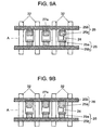
- Fig. 9A shows an example in which recess 27a is formed closer to the scan electrode relative to discharge gap 24 in order to increase the area in which recess 27a and display electrode 26 that serves as the scan electrode face each other.
- Fig. 9B shows an example in which recess 27a is formed in a manner such that a part of it is located on bus electrode 25b of the scan electrode in order to enhance the above-mentioned advantage.
- the shape of recess 27a may be as shown in Fig. 8A to Fig. 8C.
- the shape of recess 27a can be polygonal, circular, or oval and is not limited to what is described above so far as the above object can be achieved.
- Fig. 11 is a partial perspective view of a front panel of the plasma display panel in Preferred Embodiment - 2 of the present invention.
- two recesses 27c and 27d are formed in each discharge cell on the surface of a discharge space of dielectric layer 27 that covers display electrodes 26.
- Fig. 12 illustrates the positional relationship among recess 27c, recess 27d, display electrodes 26 and ribs 32. As illustrated in Fig. 12, recess 27c and recess 27d are formed in between ribs 32.
- Display electrodes 26 are comprised of discharge electrodes 25a consisting of transparent electrodes that are opposingly formed with discharge gap 24 interposed for each display line A and bus electrodes 25b for supplying power to discharge electrodes 25a.
- Discharge electrodes 25a in a discharge cell are formed in a manner projecting out in the direction orthogonal to bus electrodes 25b so that they face each other with discharge gap 24 interposed.
- One of discharge electrodes 25a in a discharge cell is situated in the bottom region of recess 27c while the other faces the bottom region of recess 27d.
- the width, W25a, of discharge electrodes 25a that face each other with discharge gap 24 interposed is made equal to or smaller than the width W27c of recess 27c and width W27d of recess 27d.
- Fig. 12 illustrates an example in which the width (W25a) of that part of discharge electrodes 25a which oppose each other with discharge gap 24 interposed is made smaller than the width (W27c, W27d) of recesses 27
- Fig. 13 is an illustration of the advantage of forming two recesses 27c, 27d on dielectric layer 27 in the plasma display panel of Preferred Embodiment - 2.
- solid line A represents a discharge.
- Discharge electrodes 25a in a discharge cell as illustrated in Fig. 14 represent a configuration in which they are divided into a plurarity of parts. Discharge electrodes 25a in a discharge cell shown in Fig. 15 are made hollow by gouging out discharge electrodes 25a as shown in Fig. 12. By decreasing the area of the discharge electrodes in this way, similar advantage as described in Preferred Embodiment - 1 in reference to Fig. 4 and Fig. 5 can be obtained.
- recess 27c and recess 27d are not limited to rectangles as shown in Fig. 12. In so far as the width of recess 27c and recess 27d is greater than the width of the part that faces discharge electrodes 25a with discharge gap 24 interposed, the shape does not matter.
- Fig. 16A and Fig 16B illustrate examples of other shapes of recess 27c and recess 27d.
- the shape of recess 27c and recess 27d as shown in Fig. 16A is a rectangle with rounded corners.
- Recess 27c and recess 27d as shown in Fig. 16B differ in size.
- Fig. 17A illustrates an example of a structure in which the area that recess 27c opposes the scan electrode is made greater by making the size of recess 27c greater than that of recess 27d. Also, Fig.
- FIG. 17B illustrates an example of a structure in which the overlapping area of recess 27c and discharge electrode 25a is made greater than the overlapping area of recess 27d and discharge electrode 25a by forming them closer to the scan electrode relative to discharge gap 24, although the sizes of recess 27c and recess 27d are the same.
- Fig. 17C illustrates an example of a structure in which a part of recess 27c is formed on bus electrode 25b of the scan electrode in order to enhance the above-described advantage.
- the shapes of recess 27c and recess 27d may be like those illustrated in Fig. 16A and Fig. 16B.
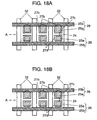
- Fig. 18A shows an example of partly extended recess 27b that has a curved protrusion. Also, in Fig. 18B, an example of partly extended recess 27b having a pointed shape is shown.
- FIG. 19A to Fig. 19C other embodiments of the recess are shown in Fig. 19A to Fig. 19C.
- at least one groove 27e is formed that connects recess 27c and recess 27d for each afore-described discharge cell. In this case, compatibility of a reduction in the discharge starting voltage and an increase in the discharge distance is obtained.
- two recesses 27c, 27d are formed parallel to each other in the direction orthogonal to bus electrodes 25b. In this case, the discharge starting voltage can be reduced.
- at least one groove 27e is formed that connects recess 27c and recess 27d shown in Fig. 19B.
- the shape of the recesses is not limited to what is described above.
- discharge can be controlled while the driving during the addressing period can be stabilized. Also, the efficiency improvement due to a high xenon (Xe) partial pressure can be effectively utilized enabling improvements in the panel efficiency and picture quality.
- Xe xenon
Landscapes
- Engineering & Computer Science (AREA)
- Physics & Mathematics (AREA)
- Plasma & Fusion (AREA)
- Chemical & Material Sciences (AREA)
- Materials Engineering (AREA)
- Gas-Filled Discharge Tubes (AREA)
Abstract
A recess (27a) is formed on the surface of each discharge cell of a dielectric layer which is covering display electrodes (26). Discharge electrodes (25a) are formed to project towards the discharge gap (24), and to face each other through the discharge gap.
Description
The present invention relates to plasma display devices
known as display devices.
In recent years, there has been an increasing expectation on
large-shield wall-hung television for use as bidirectional
information terminals. As display devices for this purpose, many
types of displays are available such as liquid crystal display panel,
field emission display and electroluminescent display. Among them,
plasma display panel (hereinafter referred to as PDP) is drawing
attention as a flat display device with good visibility because of
self-luminescence, ability to display beautiful pictures, and ease of
realizing larger shield sizes, and efforts are being made to achieve
higher definition and larger shield sizes.
The driving schemes of PDP can be broadly divided into AC
type and DC type. Thebacke two types of discharge schemes,
namely, surface discharge type and opposing discharge type.
Currently, AC type and surface discharge type PDP's are dominant
from the standpoints of achieving higher definition and larger shield,
and simplicity of manufacturing.
Fig. 20 shows an example of a conventional PDP panel
structure. As illustrated in Fig. 20, the PDP is comprised of front
panel 1 and back panel 2.
Here, scan electrode 4 and sustain electrode 5 consist of
transparent electrodes 4a, 5a that serve as discharge electrodes and
bus electrodes 4b, 5b that are electrically connected with
transparent electrodes 4a, 5a, respectively. Bus electrodes 4b, 5b
are formed with such material as Cr/Cu/Cr, Ag or the like.
front and
The discharge space of this PDP is partitioned into a plurality of
sections by barrier ribs 12, and a plurality of discharge cells or
light-emitting pixel regions is each defined by barrier ribs 12 and display
and address electrodes 6, 10 that are orthogonal to each other.
With this PDP, discharge is caused by periodic application of voltage
to address electrode 10 and display electrode 6, and ultraviolet rays
generated by this discharge are applied to phosphor layer 13, thereby being
converted into visible light. In this way, an image is displayed.
As shown in FIG. 14, scan and sustain electrodes 4, 5 of display
electrode 6 are disposed with discharging gap 14 between these electrodes 4,
5. Light-emitting pixel region 15 is a region surrounded by this display
electrode 6 and barrier ribs 12, and non-light-emitting pixel region 16 is an
adjoining gap or region between adjacent display electrodes 6. Also, a
black stripe is sometimes formed in non-light-emitting pixel region 16
for the purpose of improving the contrast.
For the development of PDP, further effort toward higher
luminance, higher efficiency, lower power consumption, and lower
cost are essential. In order to achieve a higher efficiency, it is
essential to control discharge in each region of light-emitting pixel.
Especially in the area of spread of discharge perpendicular to
display electrodes 6, as bus electrodes 4b, 5b shield the light
emitted by the phosphor, it is effective to control discharge from
spreading to the shielded area.
As an approach to efficiency improvement, a method is known,
as disclosed in Japanese Patent Laid-Open Application No.
H8-250029, for example, in which the discharge in the area shielded
by bus electrodes 4b, 5b is suppressed by increasing the thickness of
dielectric layer 7 on bus electrodes 4b, 5b.
However, in the conventional structure as described above,
although the discharge in the direction perpendicular to the display
electrodes is suppressed, the discharge in the direction parallel to
the display electrodes is not suppressed and spreads to the
neighborhood of barrier ribs. In this case, there is a possibility of
lowering of the electron temperature due to ribs and reduction in
the efficiency due to occurrence of recombination of electrons and
ions.
The plasma display device of the present invention includes a
pair of front substrate and a back substrate that are opposingly
disposed in a manner such that discharge spaces partitioned by ribs
are formed between the substrates, a pair of display electrodes
comprising discharge electrodes that are opposingly disposed on the
front substrate for each display line with discharge gaps interposed
in a manner such that discharge cells are formed between the ribs
and bus electrodes for supplying power to the discharge electrodes,
and a dielectric layer formed in a manner covering the display
electrodes, where the dielectric layer has at least one recess formed
on the surface on the side of the discharge space of each discharge
cell, and the discharge electrodes are formed in a manner projecting
out from the bus electrodes toward the discharge gap in a manner
opposing to each other in the bottom region of the recess with the
discharge gap interposed.
With this structure, luminous efficiency can be improved and
driving of the panel can be stabilized.
Referring to drawings, a description of the plasma display
devices in preferred embodiments of the present invention will now
be given below. In the drawings, similar structural components
have the same reference numerals.
Fig. 1 is a sectional perspective view of an example of panel
structure of a plasma display panel as used in the plasma display
device in Preferred Embodiment - 1 of the present invention.
As illustrated in Fig. 1, the PDP consists of front panel 21
and back panel 22.
This discharge space is divided by rib 32 into a plurarity of
sections and an discharge cell, being a unitary light-emmitting
region, is formed at the place where display electrodes 26 and
address electrodes 30 intersect at right angles.
Also, black stripes may be formed between discharge cells for
the purpose of improving contrast.
With this PDP, discharge is caused by periodic application of voltage
to address electrodes 30 and display electrodes 26, and ultraviolet rays
generated by this discharge are applied to phosphor layer 13, thereby being
converted into visible light. In this way, an image is displayed.
Fig. 2 is a sectional perspective view of the front panel of a
plasma display device in Preferred Embodiment - 1 of the present
invention. In Fig. 2, recess 27a is formed for each discharge cell on
the surface on the side of the discharge space of dielectric layer 27
that is formed on front substrate 23 in a manner covering display
electrodes 26.
Fig. 3 illustrates the positional relationship among recess 27a,
display electrodes 26, and ribs 32. As shown in Fig. 3, recess 27a is
formed between ribs 32.
Here, in order to achieve a higher efficiency of the PDP, it is
essential to control discharge in each region of light-emitting pixel.
Especially in the region in which discharge in the direction
perpendicular to display electrodes 26 spreads, as bus electrodes
25b shield the light from phosphor 33 thus making it useless, it is
effective to control the discharge from spreading to the region to be
shielded.
It is also effective for efficiency improvement to control not
only the discharge in the direction perpendicular to display
electrodes 26 but also the discharge in the parallel direction. This
is because, when the discharge spreads in the direction parallel to
display electrodes 26 up to the neighborhood of ribs 32, electron
temperature decreases near ribs 32 thus presenting a possibility of
a reduction in the efficiency.
Furthermore, when discharge takes place near ribs 32, ribs
32 are negatively charged and positive ions are attracted to ribs 32.
As a result, ribs 32 are etched by occurrence of recombination of
electrons and ions and by ion bombardment of ribs 32. There is a
possibility that a portion of ribs 32 that are etched precipitates on
phosphor 33 thus deteriorating the characteristic.
However, in this preferred embodiment, recess 27a is formed
for each individual discharge cell and recess 27a is located between
adjacent ribs 32, or the width of recess 27a is smaller than the
distance between adjacent ribs 32. By forming recess 27a in this
manner, discharge can be retained only in the bottom region of
recess 27a. That is, the discharge can be deterred from spreading
in the direction perpendicular to display electrodes 26 up to bus
electrodes 25b where the light from phosphor 33 is shielded or
spreading in the direction parallel to display electrodes 26 to the
neighborhood of ribs 32. Furthermore, as MgO is applied on the
sides of recess 27a, too, there is no possibility of the sides of recess
27a being etched. Still more, as discharge electrodes 25a in a
discharge cell are situated in the bottom region of recess 27a and
are formed in a manner projecting out in the direction orthogonal to
bus electrodes 25b so that they face each other with discharge gap
24 interposed, discharge electrodes 25a in an discharge cell are at a
distance from ribs 32. As a result, the accumulation of electric
charges in the neighborhood of ribs 32 is suppressed, and the
advantage of suppressing discharge in the neighborhood of ribs 32 is
further enhanced.
Here, when discharge electrodes 25a are formed with
transparent electrodes, the light emission from phosphor 33 can be
efficiently taken out.
On the contrary, when discharge electrodes 25a are formed
with opaque metal electrodes similar to bus electrodes 25b, a cost
reduction can be achieved. In this case, however, the light
emission from phosphor 33 is shielded by discharge electrodes 25a.
It is possible, though, to improve the efficiency of taking out the
light emission by making the area of discharge electrodes 25a in the
discharge cell small without changing the dimension of discharge
gap 24. Examples of such structures are illustrated in Fig. 4 and
Fig. 5.
Next, a description on the control of the discharge region will
be given in reference to Fig. 6 and Fig. 7. Fig. 6 is a cross-sectional
view of a schematic structure of the front panel for illustrating the
discharging state of a plasma display device in Preferred
Embodiment - 1. Fig. 7 is an illustration of the discharging state
of a conventional plasma display device.
In the conventional structure of Fig. 7 that does not have
recesses, as the thickness of the dielectric layer is uniform,
capacitance C is uniform over the surface of dielectric layer 27, and
discharge B spreads as shown in Fig. 7. Accordingly, the efficiency
decreases for the reason described above.
On the contrary, as shown in Fig. 6, recess 27a is formed for
each discharge cell thereby to make the thickness of that part of
dielectric layer 27 thin and to increase capacitance C. As a result,
charges for discharge are collectively formed in the bottom region of
recess 27a. Also, as the thickness of dielectric layer 27 of the part
where recess 27a is formed is thinner than other parts, discharge
starts to take place in the bottom region of recess 27a.
Conversely speaking, as the thickness of dielectric layer 27a
becomes thicker except the bottom region of recess 27a, the
capacitance of that part becomes smaller. That is, the electric
charges that exist in the thick part are fewer. Furthermore, as the
thickness of dielectric layer 27 is thicker, the discharge voltage is
higher.
In addition, by projecting out discharge electrodes 25a in a
discharge cell in adaptation to the shape of recess 27a and
separating them from ribs 32, the electric charges that accumulate
in the neighborhood of ribs 32 are also suppressed.
As a result of these advantages, discharge A is restricted to
the bottom region of recess 27a and the efficiency is improved. Also,
by applying this principle, it is possible to arbitrarily control the
amount of electric charges that are formed in recess 27a by
changing the size of recess27a.
Also, it is generally known to increase the partial pressure of
xenon (Xe) used as the discharge gas in order to achieve a higher
efficiency of a PDP. However, when the partial pressure of xenon
(Xe) is increased, not only the problem of increase in discharge
voltage occurs, but also the problem of causing easy saturation of
luminance occurs due to an increase in ultraviolet rays that are
produced. In order to avoid this, a method is known to decrease the
capacitance of the dielectric layer by increasing the thickness of the
dielectric layer so as to decrease the electric charges that are
generated by a single pulse. In this case, however, a problem of
efficiency reduction occurs as the transmissivity of the dielectric
layer itself decreases with increasing thickness of the dielectric
layer. Also, when the thickness is simply increased, a problem of
further increase in the discharge voltage occurs.
However, according to the present invention, a discharge gas
that is a mixture of xenon (Xe), neon (Ne) and/or helium (He) is
filled in the discharge space with the partial pressure of xenon (Xe)
set to a range 5 to 30%. And, by controlling the current with the
shape of recess 27a, prevention of luminance saturation that would
otherwise occur at high xenon (Xe) partial pressure is enabled.
Also, by changing the shape or size of recess 27a, the amount of
current can be limited to an arbitrary value. Furthermore, in this
preferred embodiment, as the current is controlled by dielectric
layer 27 only, high xenon (Xe) partial pressure can be used without
calling for a change in the circuit or driving method.
Here, the shape of recess 27a is not limited to rectangles as
shown in Fig. 3 and any shape is acceptable in so far as the width,
W27a, is greater than the width, W25a, of the part that discharge
electrodes 25a face each other with the discharge gap 24 interposed.
Fig. 8A to Fig. 8C show examples of other shapes of recess 27a.
The shape of recess 27a as shown in Fig. 8A is a rectangle with
rounded corners. The shape of recess 27a as shown in Fig. 8B is a
trapezoid. The shape of the recess as shown in Fig. 8C is a
trapezoid with roundish sides. The shape includes oval or
barrel-shaped shapes.
Also, by making the area of recess 27a on the side of the scan
electrode, being one of the display electrodes 26, larger, discharge
between the scan electrodes and address electrodes 30 is made easy
to take place thus making it possible to widen the driving margin of
the panel. Examples of such configurations are shown in Fig. 9A
and Fig. 9B. Fig. 9A shows an example in which recess 27a is
formed closer to the scan electrode relative to discharge gap 24 in
order to increase the area in which recess 27a and display electrode
26 that serves as the scan electrode face each other. Fig. 9B shows
an example in which recess 27a is formed in a manner such that a
part of it is located on bus electrode 25b of the scan electrode in
order to enhance the above-mentioned advantage. In these
structures, too, the shape of recess 27a may be as shown in Fig. 8A
to Fig. 8C.
Here, in the structure as shown in Fig. 9B, as the thickness
of dielectric layer 27 becomes smaller on the part of bus electrode
25b due to recess 27a, there is a possibility of the dielectric
breakdown strength of dielectric layer 27 being reduced on that part.
Accordingly, it is preferable to form the part of recess 27a that is
located on bus electrode 25b be as small as possible. In order to do
this, extended recess 27b made by protruding a part of recess 27a is
formed in a manner facing bus electrode 25b. For example, curved
extended recess 27b as illustrated in Fig. 10A is formed. Also,
pointed extended recess 27b is formed as illustrated in Fig. 10B.
In the above description, the shape of recess 27a can be
polygonal, circular, or oval and is not limited to what is described
above so far as the above object can be achieved.
Referring to drawings, a description of a plasma display
device in Preferred Embodiment - 2 of the present invention will be
given. The difference of structure from that of Preferred
Embodiment - 1 of the present invention lies in the configuration of
the recess. In the following, a detailed description of the difference
will be given. The same reference numerals are given to those
structural elements that are similar to those in Preferred
Embodiment - 1.
Fig. 11 is a partial perspective view of a front panel of the
plasma display panel in Preferred Embodiment - 2 of the present
invention. In Fig. 11, two recesses 27c and 27d are formed in each
discharge cell on the surface of a discharge space of dielectric layer
27 that covers display electrodes 26. Also, Fig. 12 illustrates the
positional relationship among recess 27c, recess 27d, display
electrodes 26 and ribs 32. As illustrated in Fig. 12, recess 27c and
recess 27d are formed in between ribs 32.
Fig. 13 is an illustration of the advantage of forming two
recesses 27c, 27d on dielectric layer 27 in the plasma display panel
of Preferred Embodiment - 2. In Fig. 13, solid line A represents a
discharge.
In Fig. 13, as the thickness of that part of dielectric layer 27
where two recesses 27c, 27d are formed is thin, capacitance C of
that part is large. As a result, charges for discharge are
collectively formed in the bottom regions of recess 27c and recess
27d thereby limiting the discharging region.
Furthermore, in this structure, two recesses 27c and 27d are
formed with discharge gap 24 interposed as shown in Fig. 13.
Discharge A takes place between the bottom region of recess 27c
and the bottom region of recess 27d with discharge gap 24
interposed. As a result, the discharge distance is extended, the
probability of exciting the discharge gas is increased, thus providing
the compatibility of control of discharge and high efficiency. This
effect is more pronounced when the partial pressure of xenon (Xe) in
the discharge gas is increased.
Here, the shapes of recess 27c and recess 27d are not limited
to rectangles as shown in Fig. 12. In so far as the width of recess
27c and recess 27d is greater than the width of the part that faces
discharge electrodes 25a with discharge gap 24 interposed, the
shape does not matter.
Fig. 16A and Fig 16B illustrate examples of other shapes of
recess 27c and recess 27d. The shape of recess 27c and recess 27d
as shown in Fig. 16A is a rectangle with rounded corners. Recess
27c and recess 27d as shown in Fig. 16B differ in size.
Also, by forming one of recess 27c and recess 27d that oppose
display electrode 26 to be used as a scan electrode in a manner such
that the opposing area is greater, discharge between the scan
electrode and address electrode 30 is made easy to take place during
addressing operation. That is, driving margin of the panel can be
widened. Examples of such structures are shown in Fig. 17A to Fig.
17C. Fig. 17A illustrates an example of a structure in which the
area that recess 27c opposes the scan electrode is made greater by
making the size of recess 27c greater than that of recess 27d. Also,
Fig. 17B illustrates an example of a structure in which the
overlapping area of recess 27c and discharge electrode 25a is made
greater than the overlapping area of recess 27d and discharge
electrode 25a by forming them closer to the scan electrode relative
to discharge gap 24, although the sizes of recess 27c and recess 27d
are the same. Also, Fig. 17C illustrates an example of a structure
in which a part of recess 27c is formed on bus electrode 25b of the
scan electrode in order to enhance the above-described advantage.
Here again, the shapes of recess 27c and recess 27d may be like
those illustrated in Fig. 16A and Fig. 16B.
Here, in the case of a structure as shown in Fig. 17C, the
thickness of dielectric layer 27 becomes thin because of that part of
recess 27c which overlaps bus electrode 25b. For this reason, there
is a possibility that the dielectric breakdown strength of dielectric
layer 27 of this part is reduced. Therefore, it is preferable to form
that part of recess 27c which overlaps bus electrode 25b to a
smallest possible size. For this purpose, recess 27c having partly
protruding extended recess 27b is formed and the bottom region of
partly extended recess 27b is situated on bus electrode 25b. To be
more specific, Fig. 18A shows an example of partly extended recess
27b that has a curved protrusion. Also, in Fig. 18B, an example of
partly extended recess 27b having a pointed shape is shown.
Also, other embodiments of the recess are shown in Fig. 19A
to Fig. 19C. In the example shown in Fig. 19A, at least one groove
27e is formed that connects recess 27c and recess 27d for each
afore-described discharge cell. In this case, compatibility of a
reduction in the discharge starting voltage and an increase in the
discharge distance is obtained. In the example shown in Fig. 19B,
two recesses 27c, 27d are formed parallel to each other in the
direction orthogonal to bus electrodes 25b. In this case, the
discharge starting voltage can be reduced. Furthermore, in the
example shown in Fig. 19C, at least one groove 27e is formed that
connects recess 27c and recess 27d shown in Fig. 19B.
In the above, although a description was made on an example
of forming two recesses 27c, 27d, more than two recesses may be
made and the shape of the recesses may be polygonal, circular, or
oval. In so far as the above object can be achieved, the shape of the
recess is not limited to what is described above.
With the plasma display device in accordance with the
present invention, discharge can be controlled while the driving
during the addressing period can be stabilized. Also, the efficiency
improvement due to a high xenon (Xe) partial pressure can be
effectively utilized enabling improvements in the panel efficiency
and picture quality.
Claims (14)
- A plasma display device comprising:a pair of a front substrate and a back substrate that are opposingly disposed in a manner such that an discharge space divided by ribs between the substrates is formed;a pair of display electrodes comprising discharge electrodes that are opposingly disposed on the front substrate for each displaying line with an discharge gap interposed and a bus electrode for supplying power to the discharge electrodes such that an discharge cell is formed between the ribs; anda dielectric layer formed in a manner covering the display electrodes; whereinat least one recess is formed on the dielectric layer on the surface on the side of the discharge space of each discharge cell, and the discharge electrodes are formed in a manner projecting out from the bus electrode toward the discharge gap in order that the discharge electrodes oppose each other in the bottom region of the recess with the discharge gap interposed.
- The plasma display device of claim 1, wherein the width of the discharge electrodes that oppose each other in the bottom region of the recess with the discharge gap interposed is equal to or smaller than the width of the recess.
- The plasma display device of claim 1, wherein the discharge electrodes that oppose each other in the bottom region of the recess with the discharge gap interposed is divided into plurarity.
- The plasma display device of claim 1, wherein the discharge electrodes that oppose each other in the bottom region of the recess with the discharge gap interposed is removed.
- The plasma display device of claim 1, wherein the discharge electrodes are transparent electrodes.
- The plasma display device of claim 1, wherein an discharge gas to be filled in the discharge space is a mixed gas containing xenon (Xe) and at least one of neon (Ne) and helium (He), and the partial pressure of Xe is in the range 5 to 30%.
- The plasma display device of claim 1, wherein the recess is asymmetrical with respect to the discharge gap.
- The plasma display device of claim 1, wherein the recess is formed in a manner such that the area of the part situated on one of the display electrodes is greater than the area of the part situated on the other of the display electrodes.
- The plasma display device of claim 1, wherein the recess is formed closer to one of the display electrodes with respect to the discharge gap.
- The plasma display device of claim 1, wherein the recess is formed in a manner such that the bottom region of the recess is situated on a bus electrode of one of the display electrodes.
- The plasma display device of claim 10, wherein the recess is formed in a manner such that an extended recess is formed on a part of the recess and a bottom region of the extended recess is situated on a bus electrode of one of the display electrodes.
- The plasma display device of claim 1, wherein two recesses are formed in a manner such that a bottom region of one of the recesses is situated on a bus electrode of one of the display electrodes.
- The plasma display device of claim 12, wherein one of the recesses has an extended recess formed on a part of the recess and a bottom region of the extended recess is situated on a bus electrode of one of the display electrodes.
- The plasma display device of claim 1, wherein two recesses are formed and the two recesses are connected by at least one groove.
Applications Claiming Priority (9)
| Application Number | Priority Date | Filing Date | Title |
|---|---|---|---|
| JP2002115857 | 2002-04-18 | ||
| JP2002115857 | 2002-04-18 | ||
| JP2002115855 | 2002-04-18 | ||
| JP2002115856A JP4134589B2 (en) | 2002-04-18 | 2002-04-18 | Plasma display device |
| JP2002115858A JP4178827B2 (en) | 2002-04-18 | 2002-04-18 | Plasma display device |
| JP2002115855A JP4134588B2 (en) | 2002-04-18 | 2002-04-18 | Plasma display device |
| JP2002115856 | 2002-04-18 | ||
| JP2002115858 | 2002-04-18 | ||
| PCT/JP2003/004899 WO2003088298A1 (en) | 2002-04-18 | 2003-04-17 | Plasma display |
Publications (2)
| Publication Number | Publication Date |
|---|---|
| EP1406287A1 true EP1406287A1 (en) | 2004-04-07 |
| EP1406287A4 EP1406287A4 (en) | 2008-09-10 |
Family
ID=29255484
Family Applications (1)
| Application Number | Title | Priority Date | Filing Date |
|---|---|---|---|
| EP03717633A Withdrawn EP1406287A4 (en) | 2002-04-18 | 2003-04-17 | PLASMA SCREEN |
Country Status (4)
| Country | Link |
|---|---|
| US (1) | US7071623B2 (en) |
| EP (1) | EP1406287A4 (en) |
| CN (1) | CN1301527C (en) |
| WO (1) | WO2003088298A1 (en) |
Cited By (1)
| Publication number | Priority date | Publication date | Assignee | Title |
|---|---|---|---|---|
| US7781972B2 (en) | 2005-05-11 | 2010-08-24 | Lg Electronics Inc. | Plasma display panel |
Families Citing this family (7)
| Publication number | Priority date | Publication date | Assignee | Title |
|---|---|---|---|---|
| KR20050028182A (en) * | 2003-09-17 | 2005-03-22 | 삼성에스디아이 주식회사 | Method of plasma discharge and plasma display using the same |
| KR100615210B1 (en) * | 2004-02-20 | 2006-08-25 | 삼성에스디아이 주식회사 | Plasma display panel |
| KR20050114059A (en) * | 2004-05-31 | 2005-12-05 | 삼성에스디아이 주식회사 | Plasma display panel |
| KR100673437B1 (en) * | 2004-12-31 | 2007-01-24 | 엘지전자 주식회사 | Plasma display panel |
| KR20070006103A (en) * | 2005-07-07 | 2007-01-11 | 삼성에스디아이 주식회사 | Plasma Display Panel With Field Concentrator |
| KR100719557B1 (en) * | 2005-08-13 | 2007-05-17 | 삼성에스디아이 주식회사 | Electrode terminal structure and plasma display panel having same |
| KR100719595B1 (en) * | 2005-12-30 | 2007-05-18 | 삼성에스디아이 주식회사 | Plasma display panel |
Family Cites Families (17)
| Publication number | Priority date | Publication date | Assignee | Title |
|---|---|---|---|---|
| JP3224486B2 (en) * | 1995-03-15 | 2001-10-29 | パイオニア株式会社 | Surface discharge type plasma display panel |
| USRE38357E1 (en) * | 1995-03-15 | 2003-12-23 | Pioneer Corporation | Surface discharge type plasma display panel |
| JP3655947B2 (en) * | 1995-07-19 | 2005-06-02 | パイオニア株式会社 | Surface discharge type plasma display panel |
| JP3547267B2 (en) * | 1996-09-13 | 2004-07-28 | パイオニア株式会社 | Surface discharge type plasma display panel |
| JP3106992B2 (en) * | 1997-02-20 | 2000-11-06 | 日本電気株式会社 | AC surface discharge type plasma display panel |
| US6433477B1 (en) * | 1997-10-23 | 2002-08-13 | Lg Electronics Inc. | Plasma display panel with varied thickness dielectric film |
| KR100252990B1 (en) * | 1997-10-24 | 2000-04-15 | 구자홍 | Color plasma display panel with arc discharge electrode |
| JPH11212515A (en) * | 1998-01-21 | 1999-08-06 | Hitachi Ltd | Plasma display device |
| TW423006B (en) * | 1998-03-31 | 2001-02-21 | Toshiba Corp | Discharge type flat display device |
| JP3688114B2 (en) * | 1998-04-14 | 2005-08-24 | パイオニア株式会社 | Plasma display panel |
| JP4205247B2 (en) * | 1999-03-30 | 2009-01-07 | 株式会社日立製作所 | Plasma display device |
| KR100432998B1 (en) * | 1999-07-09 | 2004-05-24 | 삼성에스디아이 주식회사 | plasma display panel |
| JP2001160361A (en) * | 1999-09-21 | 2001-06-12 | Mitsubishi Electric Corp | Plasma display panel substrate and plasma display panel |
| JP2001118520A (en) | 1999-10-19 | 2001-04-27 | Matsushita Electric Ind Co Ltd | Gas discharge panel |
| CN101090054B (en) * | 2000-01-26 | 2010-05-26 | 松下电器产业株式会社 | Surface discharge type display device with excellent power consumption suppression effect |
| EP1381071B1 (en) * | 2002-01-28 | 2010-04-28 | Panasonic Corporation | Plasma display device |
| FR2841378A1 (en) * | 2002-06-24 | 2003-12-26 | Thomson Plasma | COPLANAR DISCHARGE SLAB FOR PLASMA VIEWING PANEL PROVIDING AN ADAPTED SURFACE POTENTIAL DISTRIBUTION |
-
2003
- 2003-04-17 US US10/485,215 patent/US7071623B2/en not_active Expired - Fee Related
- 2003-04-17 EP EP03717633A patent/EP1406287A4/en not_active Withdrawn
- 2003-04-17 WO PCT/JP2003/004899 patent/WO2003088298A1/en not_active Ceased
- 2003-04-17 CN CNB038011077A patent/CN1301527C/en not_active Expired - Fee Related
Cited By (1)
| Publication number | Priority date | Publication date | Assignee | Title |
|---|---|---|---|---|
| US7781972B2 (en) | 2005-05-11 | 2010-08-24 | Lg Electronics Inc. | Plasma display panel |
Also Published As
| Publication number | Publication date |
|---|---|
| EP1406287A4 (en) | 2008-09-10 |
| US20040207324A1 (en) | 2004-10-21 |
| WO2003088298A1 (en) | 2003-10-23 |
| US7071623B2 (en) | 2006-07-04 |
| CN1301527C (en) | 2007-02-21 |
| CN1557010A (en) | 2004-12-22 |
Similar Documents
| Publication | Publication Date | Title |
|---|---|---|
| US7352129B2 (en) | Plasma display panel | |
| US7071623B2 (en) | Plasma display | |
| CN100483604C (en) | Plasma display device | |
| US7615927B2 (en) | Low address discharge voltage plasma display panel | |
| JP2005347250A (en) | Plasma display panel | |
| US7183711B2 (en) | Plasma display panel and video display system employing same | |
| KR20050051039A (en) | Plasma display panel | |
| JP3994626B2 (en) | Plasma display panel | |
| JP2004006307A (en) | Plasma display device | |
| US7538494B2 (en) | Plasma display panel | |
| JP4178827B2 (en) | Plasma display device | |
| JP3772747B2 (en) | Plasma display device | |
| EP1601000B1 (en) | Plasma display panel | |
| JP4134588B2 (en) | Plasma display device | |
| KR100586112B1 (en) | Plasma display device | |
| JP4395142B2 (en) | Plasma display panel | |
| US20070007890A1 (en) | Plasma display panel | |
| KR20020061795A (en) | The Plasma display panel | |
| KR19990077963A (en) | Improvements to AC Plasma Display Panels | |
| JP4134589B2 (en) | Plasma display device | |
| JP2003132798A (en) | Plasma display panel | |
| JP2001283737A (en) | Plasma display panel | |
| JP2001006564A (en) | Plasma display panel | |
| JP2006190678A (en) | Plasma display device | |
| JP2005197260A (en) | Plasma display panel |
Legal Events
| Date | Code | Title | Description |
|---|---|---|---|
| PUAI | Public reference made under article 153(3) epc to a published international application that has entered the european phase |
Free format text: ORIGINAL CODE: 0009012 |
|
| 17P | Request for examination filed |
Effective date: 20040114 |
|
| AK | Designated contracting states |
Kind code of ref document: A1 Designated state(s): AT BE BG CH CY CZ DE DK EE ES FI FR GB GR HU IE IT LI LU MC NL PT RO SE SI SK TR |
|
| A4 | Supplementary search report drawn up and despatched |
Effective date: 20080808 |
|
| RAP1 | Party data changed (applicant data changed or rights of an application transferred) |
Owner name: PANASONIC CORPORATION |
|
| 17Q | First examination report despatched |
Effective date: 20081119 |
|
| STAA | Information on the status of an ep patent application or granted ep patent |
Free format text: STATUS: THE APPLICATION IS DEEMED TO BE WITHDRAWN |
|
| 18D | Application deemed to be withdrawn |
Effective date: 20120320 |