EP1400850A1 - Method of forming thick resist pattern - Google Patents
Method of forming thick resist pattern Download PDFInfo
- Publication number
- EP1400850A1 EP1400850A1 EP02733301A EP02733301A EP1400850A1 EP 1400850 A1 EP1400850 A1 EP 1400850A1 EP 02733301 A EP02733301 A EP 02733301A EP 02733301 A EP02733301 A EP 02733301A EP 1400850 A1 EP1400850 A1 EP 1400850A1
- Authority
- EP
- European Patent Office
- Prior art keywords
- group
- radiation sensitive
- resist pattern
- resin composition
- thick film
- Prior art date
- Legal status (The legal status is an assumption and is not a legal conclusion. Google has not performed a legal analysis and makes no representation as to the accuracy of the status listed.)
- Withdrawn
Links
- 238000000034 method Methods 0.000 title claims description 22
- 229920005989 resin Polymers 0.000 claims abstract description 58
- 239000011347 resin Substances 0.000 claims abstract description 58
- 230000005855 radiation Effects 0.000 claims abstract description 51
- 239000011342 resin composition Substances 0.000 claims abstract description 48
- 239000000203 mixture Substances 0.000 claims abstract description 27
- 239000003504 photosensitizing agent Substances 0.000 claims abstract description 27
- 229920003986 novolac Polymers 0.000 claims abstract description 26
- WTQZSMDDRMKJRI-UHFFFAOYSA-N 4-diazoniophenolate Chemical group [O-]C1=CC=C([N+]#N)C=C1 WTQZSMDDRMKJRI-UHFFFAOYSA-N 0.000 claims abstract description 19
- 239000000178 monomer Substances 0.000 claims abstract description 18
- 229920001577 copolymer Polymers 0.000 claims abstract description 15
- 239000004793 Polystyrene Substances 0.000 claims abstract description 14
- 229920002223 polystyrene Polymers 0.000 claims abstract description 14
- 239000000463 material Substances 0.000 claims abstract description 12
- 125000003011 styrenyl group Chemical class [H]\C(*)=C(/[H])C1=C([H])C([H])=C([H])C([H])=C1[H] 0.000 claims abstract 3
- -1 acrylic ester Chemical class 0.000 claims description 36
- 150000002148 esters Chemical class 0.000 claims description 20
- 229920002120 photoresistant polymer Polymers 0.000 claims description 14
- JHPBZFOKBAGZBL-UHFFFAOYSA-N (3-hydroxy-2,2,4-trimethylpentyl) 2-methylprop-2-enoate Chemical compound CC(C)C(O)C(C)(C)COC(=O)C(C)=C JHPBZFOKBAGZBL-UHFFFAOYSA-N 0.000 claims description 13
- 230000032050 esterification Effects 0.000 claims description 7
- 238000005886 esterification reaction Methods 0.000 claims description 7
- ALVGSDOIXRPZFH-UHFFFAOYSA-N [(1-diazonioimino-3,4-dioxonaphthalen-2-ylidene)hydrazinylidene]azanide Chemical compound C1=CC=C2C(=N[N+]#N)C(=NN=[N-])C(=O)C(=O)C2=C1 ALVGSDOIXRPZFH-UHFFFAOYSA-N 0.000 claims description 4
- LYKRPDCJKSXAHS-UHFFFAOYSA-N phenyl-(2,3,4,5-tetrahydroxyphenyl)methanone Chemical compound OC1=C(O)C(O)=CC(C(=O)C=2C=CC=CC=2)=C1O LYKRPDCJKSXAHS-UHFFFAOYSA-N 0.000 claims description 4
- LSNNMFCWUKXFEE-UHFFFAOYSA-M Bisulfite Chemical compound OS([O-])=O LSNNMFCWUKXFEE-UHFFFAOYSA-M 0.000 claims 2
- 230000035945 sensitivity Effects 0.000 abstract description 17
- 125000002887 hydroxy group Chemical group [H]O* 0.000 abstract description 14
- 150000001875 compounds Chemical class 0.000 abstract description 10
- ISWSIDIOOBJBQZ-UHFFFAOYSA-N phenol group Chemical group C1(=CC=CC=C1)O ISWSIDIOOBJBQZ-UHFFFAOYSA-N 0.000 abstract description 9
- 238000004090 dissolution Methods 0.000 abstract description 8
- 239000000758 substrate Substances 0.000 abstract description 5
- NIXOWILDQLNWCW-UHFFFAOYSA-M Acrylate Chemical compound [O-]C(=O)C=C NIXOWILDQLNWCW-UHFFFAOYSA-M 0.000 abstract 1
- CERQOIWHTDAKMF-UHFFFAOYSA-M Methacrylate Chemical compound CC(=C)C([O-])=O CERQOIWHTDAKMF-UHFFFAOYSA-M 0.000 abstract 1
- 239000003795 chemical substances by application Substances 0.000 abstract 1
- 229920000058 polyacrylate Polymers 0.000 abstract 1
- 229920000193 polymethacrylate Polymers 0.000 abstract 1
- 150000003440 styrenes Chemical class 0.000 description 11
- WGTYBPLFGIVFAS-UHFFFAOYSA-M tetramethylammonium hydroxide Chemical compound [OH-].C[N+](C)(C)C WGTYBPLFGIVFAS-UHFFFAOYSA-M 0.000 description 8
- 238000004519 manufacturing process Methods 0.000 description 6
- 150000007524 organic acids Chemical class 0.000 description 6
- 230000000052 comparative effect Effects 0.000 description 5
- 239000004065 semiconductor Substances 0.000 description 5
- 239000004094 surface-active agent Substances 0.000 description 5
- KJCVRFUGPWSIIH-UHFFFAOYSA-N 1-naphthol Chemical compound C1=CC=C2C(O)=CC=CC2=C1 KJCVRFUGPWSIIH-UHFFFAOYSA-N 0.000 description 4
- NKTOLZVEWDHZMU-UHFFFAOYSA-N 2,5-xylenol Chemical compound CC1=CC=C(C)C(O)=C1 NKTOLZVEWDHZMU-UHFFFAOYSA-N 0.000 description 4
- NXXYKOUNUYWIHA-UHFFFAOYSA-N 2,6-Dimethylphenol Chemical compound CC1=CC=CC(C)=C1O NXXYKOUNUYWIHA-UHFFFAOYSA-N 0.000 description 4
- WSFSSNUMVMOOMR-UHFFFAOYSA-N Formaldehyde Chemical compound O=C WSFSSNUMVMOOMR-UHFFFAOYSA-N 0.000 description 4
- MWPLVEDNUUSJAV-UHFFFAOYSA-N anthracene Chemical compound C1=CC=CC2=CC3=CC=CC=C3C=C21 MWPLVEDNUUSJAV-UHFFFAOYSA-N 0.000 description 4
- 238000010586 diagram Methods 0.000 description 4
- 230000000694 effects Effects 0.000 description 4
- LYCAIKOWRPUZTN-UHFFFAOYSA-N ethylene glycol Natural products OCCO LYCAIKOWRPUZTN-UHFFFAOYSA-N 0.000 description 4
- RLSSMJSEOOYNOY-UHFFFAOYSA-N m-cresol Chemical compound CC1=CC=CC(O)=C1 RLSSMJSEOOYNOY-UHFFFAOYSA-N 0.000 description 4
- DNIAPMSPPWPWGF-UHFFFAOYSA-N monopropylene glycol Natural products CC(O)CO DNIAPMSPPWPWGF-UHFFFAOYSA-N 0.000 description 4
- QWVGKYWNOKOFNN-UHFFFAOYSA-N o-cresol Chemical compound CC1=CC=CC=C1O QWVGKYWNOKOFNN-UHFFFAOYSA-N 0.000 description 4
- IWDCLRJOBJJRNH-UHFFFAOYSA-N p-cresol Chemical compound CC1=CC=C(O)C=C1 IWDCLRJOBJJRNH-UHFFFAOYSA-N 0.000 description 4
- GHMLBKRAJCXXBS-UHFFFAOYSA-N resorcinol Chemical compound OC1=CC=CC(O)=C1 GHMLBKRAJCXXBS-UHFFFAOYSA-N 0.000 description 4
- 239000002904 solvent Substances 0.000 description 4
- 239000000126 substance Substances 0.000 description 4
- BDHFUVZGWQCTTF-UHFFFAOYSA-N sulfonic acid Chemical compound OS(=O)=O BDHFUVZGWQCTTF-UHFFFAOYSA-N 0.000 description 4
- ZRDYULMDEGRWRC-UHFFFAOYSA-N (4-hydroxyphenyl)-(2,3,4-trihydroxyphenyl)methanone Chemical compound C1=CC(O)=CC=C1C(=O)C1=CC=C(O)C(O)=C1O ZRDYULMDEGRWRC-UHFFFAOYSA-N 0.000 description 3
- ZWEHNKRNPOVVGH-UHFFFAOYSA-N 2-Butanone Chemical compound CCC(C)=O ZWEHNKRNPOVVGH-UHFFFAOYSA-N 0.000 description 3
- OGRAOKJKVGDSFR-UHFFFAOYSA-N 6-Oxy-pseudocumol Natural products CC1=CC(C)=C(C)C(O)=C1 OGRAOKJKVGDSFR-UHFFFAOYSA-N 0.000 description 3
- HEMHJVSKTPXQMS-UHFFFAOYSA-M Sodium hydroxide Chemical compound [OH-].[Na+] HEMHJVSKTPXQMS-UHFFFAOYSA-M 0.000 description 3
- YXFVVABEGXRONW-UHFFFAOYSA-N Toluene Chemical compound CC1=CC=CC=C1 YXFVVABEGXRONW-UHFFFAOYSA-N 0.000 description 3
- 239000002253 acid Substances 0.000 description 3
- 239000007864 aqueous solution Substances 0.000 description 3
- 230000006866 deterioration Effects 0.000 description 3
- ZUOUZKKEUPVFJK-UHFFFAOYSA-N diphenyl Chemical compound C1=CC=CC=C1C1=CC=CC=C1 ZUOUZKKEUPVFJK-UHFFFAOYSA-N 0.000 description 3
- 239000000243 solution Substances 0.000 description 3
- 125000004178 (C1-C4) alkyl group Chemical group 0.000 description 2
- KETQAJRQOHHATG-UHFFFAOYSA-N 1,2-naphthoquinone Chemical compound C1=CC=C2C(=O)C(=O)C=CC2=C1 KETQAJRQOHHATG-UHFFFAOYSA-N 0.000 description 2
- 229940105324 1,2-naphthoquinone Drugs 0.000 description 2
- XJKSTNDFUHDPQJ-UHFFFAOYSA-N 1,4-diphenylbenzene Chemical group C1=CC=CC=C1C1=CC=C(C=2C=CC=CC=2)C=C1 XJKSTNDFUHDPQJ-UHFFFAOYSA-N 0.000 description 2
- VJIFNNRQWNILPY-UHFFFAOYSA-N 1-methyl-4-(2-phenylphenyl)benzene Chemical group C1=CC(C)=CC=C1C1=CC=CC=C1C1=CC=CC=C1 VJIFNNRQWNILPY-UHFFFAOYSA-N 0.000 description 2
- QPUYECUOLPXSFR-UHFFFAOYSA-N 1-methylnaphthalene Chemical compound C1=CC=C2C(C)=CC=CC2=C1 QPUYECUOLPXSFR-UHFFFAOYSA-N 0.000 description 2
- RUFPHBVGCFYCNW-UHFFFAOYSA-N 1-naphthylamine Chemical compound C1=CC=C2C(N)=CC=CC2=C1 RUFPHBVGCFYCNW-UHFFFAOYSA-N 0.000 description 2
- WWGUMAYGTYQSGA-UHFFFAOYSA-N 2,3-dimethylnaphthalene Chemical compound C1=CC=C2C=C(C)C(C)=CC2=C1 WWGUMAYGTYQSGA-UHFFFAOYSA-N 0.000 description 2
- QWBBPBRQALCEIZ-UHFFFAOYSA-N 2,3-dimethylphenol Chemical compound CC1=CC=CC(O)=C1C QWBBPBRQALCEIZ-UHFFFAOYSA-N 0.000 description 2
- VXSCPERJHPWROZ-UHFFFAOYSA-N 2,4,5-trimethylphenol Chemical compound CC1=CC(C)=C(O)C=C1C VXSCPERJHPWROZ-UHFFFAOYSA-N 0.000 description 2
- CPEXFJVZFNYXGU-UHFFFAOYSA-N 2,4,6-trihydroxybenzophenone Chemical compound OC1=CC(O)=CC(O)=C1C(=O)C1=CC=CC=C1 CPEXFJVZFNYXGU-UHFFFAOYSA-N 0.000 description 2
- KUFFULVDNCHOFZ-UHFFFAOYSA-N 2,4-xylenol Chemical compound CC1=CC=C(O)C(C)=C1 KUFFULVDNCHOFZ-UHFFFAOYSA-N 0.000 description 2
- JWAZRIHNYRIHIV-UHFFFAOYSA-N 2-naphthol Chemical compound C1=CC=CC2=CC(O)=CC=C21 JWAZRIHNYRIHIV-UHFFFAOYSA-N 0.000 description 2
- OSOLELDZBFOFHO-UHFFFAOYSA-N 2-phenylphenanthrene Chemical compound C1=CC=CC=C1C1=CC=C2C3=CC=CC=C3C=CC2=C1 OSOLELDZBFOFHO-UHFFFAOYSA-N 0.000 description 2
- FDQQNNZKEJIHMS-UHFFFAOYSA-N 3,4,5-trimethylphenol Chemical compound CC1=CC(O)=CC(C)=C1C FDQQNNZKEJIHMS-UHFFFAOYSA-N 0.000 description 2
- YCOXTKKNXUZSKD-UHFFFAOYSA-N 3,4-xylenol Chemical compound CC1=CC=C(O)C=C1C YCOXTKKNXUZSKD-UHFFFAOYSA-N 0.000 description 2
- TUAMRELNJMMDMT-UHFFFAOYSA-N 3,5-xylenol Chemical compound CC1=CC(C)=CC(O)=C1 TUAMRELNJMMDMT-UHFFFAOYSA-N 0.000 description 2
- HMNKTRSOROOSPP-UHFFFAOYSA-N 3-Ethylphenol Chemical compound CCC1=CC=CC(O)=C1 HMNKTRSOROOSPP-UHFFFAOYSA-N 0.000 description 2
- ASHGTJPOSUFTGB-UHFFFAOYSA-N 3-methoxyphenol Chemical compound COC1=CC=CC(O)=C1 ASHGTJPOSUFTGB-UHFFFAOYSA-N 0.000 description 2
- MBGGFXOXUIDRJD-UHFFFAOYSA-N 4-Butoxyphenol Chemical compound CCCCOC1=CC=C(O)C=C1 MBGGFXOXUIDRJD-UHFFFAOYSA-N 0.000 description 2
- YEJRWHAVMIAJKC-UHFFFAOYSA-N 4-Butyrolactone Chemical compound O=C1CCCO1 YEJRWHAVMIAJKC-UHFFFAOYSA-N 0.000 description 2
- WXYSZTISEJBRHW-UHFFFAOYSA-N 4-[2-[4-[1,1-bis(4-hydroxyphenyl)ethyl]phenyl]propan-2-yl]phenol Chemical compound C=1C=C(C(C)(C=2C=CC(O)=CC=2)C=2C=CC(O)=CC=2)C=CC=1C(C)(C)C1=CC=C(O)C=C1 WXYSZTISEJBRHW-UHFFFAOYSA-N 0.000 description 2
- HXDOZKJGKXYMEW-UHFFFAOYSA-N 4-ethylphenol Chemical compound CCC1=CC=C(O)C=C1 HXDOZKJGKXYMEW-UHFFFAOYSA-N 0.000 description 2
- YQUQWHNMBPIWGK-UHFFFAOYSA-N 4-isopropylphenol Chemical compound CC(C)C1=CC=C(O)C=C1 YQUQWHNMBPIWGK-UHFFFAOYSA-N 0.000 description 2
- FNYDIAAMUCQQDE-UHFFFAOYSA-N 4-methylbenzene-1,3-diol Chemical compound CC1=CC=C(O)C=C1O FNYDIAAMUCQQDE-UHFFFAOYSA-N 0.000 description 2
- UJOBWOGCFQCDNV-UHFFFAOYSA-N 9H-carbazole Chemical compound C1=CC=C2C3=CC=CC=C3NC2=C1 UJOBWOGCFQCDNV-UHFFFAOYSA-N 0.000 description 2
- HKMTVMBEALTRRR-UHFFFAOYSA-N Benzo[a]fluorene Chemical compound C1=CC=CC2=C3CC4=CC=CC=C4C3=CC=C21 HKMTVMBEALTRRR-UHFFFAOYSA-N 0.000 description 2
- SOGAXMICEFXMKE-UHFFFAOYSA-N Butylmethacrylate Chemical compound CCCCOC(=O)C(C)=C SOGAXMICEFXMKE-UHFFFAOYSA-N 0.000 description 2
- FERIUCNNQQJTOY-UHFFFAOYSA-N Butyric acid Chemical compound CCCC(O)=O FERIUCNNQQJTOY-UHFFFAOYSA-N 0.000 description 2
- 239000004593 Epoxy Substances 0.000 description 2
- YCKRFDGAMUMZLT-UHFFFAOYSA-N Fluorine atom Chemical compound [F] YCKRFDGAMUMZLT-UHFFFAOYSA-N 0.000 description 2
- QIGBRXMKCJKVMJ-UHFFFAOYSA-N Hydroquinone Chemical compound OC1=CC=C(O)C=C1 QIGBRXMKCJKVMJ-UHFFFAOYSA-N 0.000 description 2
- SIKJAQJRHWYJAI-UHFFFAOYSA-N Indole Chemical compound C1=CC=C2NC=CC2=C1 SIKJAQJRHWYJAI-UHFFFAOYSA-N 0.000 description 2
- BAPJBEWLBFYGME-UHFFFAOYSA-N Methyl acrylate Chemical compound COC(=O)C=C BAPJBEWLBFYGME-UHFFFAOYSA-N 0.000 description 2
- UFWIBTONFRDIAS-UHFFFAOYSA-N Naphthalene Chemical compound C1=CC=CC2=CC=CC=C21 UFWIBTONFRDIAS-UHFFFAOYSA-N 0.000 description 2
- BLRPTPMANUNPDV-UHFFFAOYSA-N Silane Chemical compound [SiH4] BLRPTPMANUNPDV-UHFFFAOYSA-N 0.000 description 2
- PPBRXRYQALVLMV-UHFFFAOYSA-N Styrene Chemical compound C=CC1=CC=CC=C1 PPBRXRYQALVLMV-UHFFFAOYSA-N 0.000 description 2
- DZBUGLKDJFMEHC-UHFFFAOYSA-N acridine Chemical compound C1=CC=CC2=CC3=CC=CC=C3N=C21 DZBUGLKDJFMEHC-UHFFFAOYSA-N 0.000 description 2
- 239000000853 adhesive Substances 0.000 description 2
- 230000001070 adhesive effect Effects 0.000 description 2
- 150000001299 aldehydes Chemical class 0.000 description 2
- 125000003545 alkoxy group Chemical group 0.000 description 2
- HUMNYLRZRPPJDN-UHFFFAOYSA-N benzaldehyde Chemical compound O=CC1=CC=CC=C1 HUMNYLRZRPPJDN-UHFFFAOYSA-N 0.000 description 2
- AOJOEFVRHOZDFN-UHFFFAOYSA-N benzyl 2-methylprop-2-enoate Chemical compound CC(=C)C(=O)OCC1=CC=CC=C1 AOJOEFVRHOZDFN-UHFFFAOYSA-N 0.000 description 2
- IISBACLAFKSPIT-UHFFFAOYSA-N bisphenol A Chemical compound C=1C=C(O)C=CC=1C(C)(C)C1=CC=C(O)C=C1 IISBACLAFKSPIT-UHFFFAOYSA-N 0.000 description 2
- YCIMNLLNPGFGHC-UHFFFAOYSA-N catechol Chemical compound OC1=CC=CC=C1O YCIMNLLNPGFGHC-UHFFFAOYSA-N 0.000 description 2
- WDECIBYCCFPHNR-UHFFFAOYSA-N chrysene Chemical compound C1=CC=CC2=CC=C3C4=CC=CC=C4C=CC3=C21 WDECIBYCCFPHNR-UHFFFAOYSA-N 0.000 description 2
- JHIVVAPYMSGYDF-UHFFFAOYSA-N cyclohexanone Chemical compound O=C1CCCCC1 JHIVVAPYMSGYDF-UHFFFAOYSA-N 0.000 description 2
- 125000000113 cyclohexyl group Chemical group [H]C1([H])C([H])([H])C([H])([H])C([H])(*)C([H])([H])C1([H])[H] 0.000 description 2
- LZCLXQDLBQLTDK-UHFFFAOYSA-N ethyl 2-hydroxypropanoate Chemical compound CCOC(=O)C(C)O LZCLXQDLBQLTDK-UHFFFAOYSA-N 0.000 description 2
- XLLIQLLCWZCATF-UHFFFAOYSA-N ethylene glycol monomethyl ether acetate Natural products COCCOC(C)=O XLLIQLLCWZCATF-UHFFFAOYSA-N 0.000 description 2
- NIHNNTQXNPWCJQ-UHFFFAOYSA-N fluorene Chemical compound C1=CC=C2CC3=CC=CC=C3C2=C1 NIHNNTQXNPWCJQ-UHFFFAOYSA-N 0.000 description 2
- 239000011737 fluorine Substances 0.000 description 2
- 229910052731 fluorine Inorganic materials 0.000 description 2
- 125000000524 functional group Chemical group 0.000 description 2
- 150000004820 halides Chemical class 0.000 description 2
- CATSNJVOTSVZJV-UHFFFAOYSA-N heptan-2-one Chemical compound CCCCCC(C)=O CATSNJVOTSVZJV-UHFFFAOYSA-N 0.000 description 2
- 230000005764 inhibitory process Effects 0.000 description 2
- 125000002496 methyl group Chemical group [H]C([H])([H])* 0.000 description 2
- HDBWAWNLGGMZRQ-UHFFFAOYSA-N p-Vinylbiphenyl Chemical compound C1=CC(C=C)=CC=C1C1=CC=CC=C1 HDBWAWNLGGMZRQ-UHFFFAOYSA-N 0.000 description 2
- GPRIERYVMZVKTC-UHFFFAOYSA-N p-quaterphenyl Chemical group C1=CC=CC=C1C1=CC=C(C=2C=CC(=CC=2)C=2C=CC=CC=2)C=C1 GPRIERYVMZVKTC-UHFFFAOYSA-N 0.000 description 2
- 125000002080 perylenyl group Chemical group C1(=CC=C2C=CC=C3C4=CC=CC5=CC=CC(C1=C23)=C45)* 0.000 description 2
- YNPNZTXNASCQKK-UHFFFAOYSA-N phenanthrene Chemical compound C1=CC=C2C3=CC=CC=C3C=CC2=C1 YNPNZTXNASCQKK-UHFFFAOYSA-N 0.000 description 2
- 125000001997 phenyl group Chemical group [H]C1=C([H])C([H])=C(*)C([H])=C1[H] 0.000 description 2
- 238000000206 photolithography Methods 0.000 description 2
- 229920000642 polymer Polymers 0.000 description 2
- LLHKCFNBLRBOGN-UHFFFAOYSA-N propylene glycol methyl ether acetate Chemical compound COCC(C)OC(C)=O LLHKCFNBLRBOGN-UHFFFAOYSA-N 0.000 description 2
- BBEAQIROQSPTKN-UHFFFAOYSA-N pyrene Chemical compound C1=CC=C2C=CC3=CC=CC4=CC=C1C2=C43 BBEAQIROQSPTKN-UHFFFAOYSA-N 0.000 description 2
- 229910000077 silane Inorganic materials 0.000 description 2
- AYYISYPLHCSQGL-UHFFFAOYSA-N (2,3,4,5,6-pentachlorophenyl) 2-methylprop-2-enoate Chemical compound CC(=C)C(=O)OC1=C(Cl)C(Cl)=C(Cl)C(Cl)=C1Cl AYYISYPLHCSQGL-UHFFFAOYSA-N 0.000 description 1
- OKJFKPFBSPZTAH-UHFFFAOYSA-N (2,4-dihydroxyphenyl)-(4-hydroxyphenyl)methanone Chemical compound C1=CC(O)=CC=C1C(=O)C1=CC=C(O)C=C1O OKJFKPFBSPZTAH-UHFFFAOYSA-N 0.000 description 1
- ZDROXNKXVHPNBJ-UHFFFAOYSA-N (2,6-dihydroxyphenyl)-(2,3,4-trihydroxyphenyl)methanone Chemical compound OC1=C(O)C(O)=CC=C1C(=O)C1=C(O)C=CC=C1O ZDROXNKXVHPNBJ-UHFFFAOYSA-N 0.000 description 1
- HCNHNBLSNVSJTJ-UHFFFAOYSA-N 1,1-Bis(4-hydroxyphenyl)ethane Chemical compound C=1C=C(O)C=CC=1C(C)C1=CC=C(O)C=C1 HCNHNBLSNVSJTJ-UHFFFAOYSA-N 0.000 description 1
- OWEYKIWAZBBXJK-UHFFFAOYSA-N 1,1-Dichloro-2,2-bis(4-hydroxyphenyl)ethylene Chemical compound C1=CC(O)=CC=C1C(=C(Cl)Cl)C1=CC=C(O)C=C1 OWEYKIWAZBBXJK-UHFFFAOYSA-N 0.000 description 1
- WBBHDQPSURWWTH-UHFFFAOYSA-N 1,2,3,4,5-pentamethyl-6-(2,3,4-trimethylphenyl)benzene Chemical group CC1=C(C)C(C)=CC=C1C1=C(C)C(C)=C(C)C(C)=C1C WBBHDQPSURWWTH-UHFFFAOYSA-N 0.000 description 1
- JGPKOHSNRGXCSD-UHFFFAOYSA-N 1,2,3,4-tetramethyl-5-[4-(4-phenylphenyl)phenyl]benzene Chemical group CC1=C(C)C(C)=CC(C=2C=CC(=CC=2)C=2C=CC(=CC=2)C=2C=CC=CC=2)=C1C JGPKOHSNRGXCSD-UHFFFAOYSA-N 0.000 description 1
- JIVZDILUJCSVMN-UHFFFAOYSA-N 1,2-bis(3-methylphenyl)benzene Chemical group CC1=CC=CC(C=2C(=CC=CC=2)C=2C=C(C)C=CC=2)=C1 JIVZDILUJCSVMN-UHFFFAOYSA-N 0.000 description 1
- BRIKLJCDBBFRAE-UHFFFAOYSA-N 1,2-diphenylindole Chemical compound C=1C=CC=CC=1N1C2=CC=CC=C2C=C1C1=CC=CC=C1 BRIKLJCDBBFRAE-UHFFFAOYSA-N 0.000 description 1
- SIJHJHYRYHIWFW-UHFFFAOYSA-N 1,3,6,8-tetraphenylpyrene Chemical compound C1=CC=CC=C1C(C1=CC=C23)=CC(C=4C=CC=CC=4)=C(C=C4)C1=C2C4=C(C=1C=CC=CC=1)C=C3C1=CC=CC=C1 SIJHJHYRYHIWFW-UHFFFAOYSA-N 0.000 description 1
- IVSZLXZYQVIEFR-UHFFFAOYSA-N 1,3-Dimethylbenzene Natural products CC1=CC=CC(C)=C1 IVSZLXZYQVIEFR-UHFFFAOYSA-N 0.000 description 1
- GQHLUGQTYDTQDG-UHFFFAOYSA-N 1,7-diphenylnaphthalene Chemical compound C1=CC=CC=C1C1=CC=C(C=CC=C2C=3C=CC=CC=3)C2=C1 GQHLUGQTYDTQDG-UHFFFAOYSA-N 0.000 description 1
- IANWNOQGCKVJBO-UHFFFAOYSA-N 1-(3,3-dimethylbutoxy)-4-(4-phenylphenyl)benzene Chemical group C1=CC(OCCC(C)(C)C)=CC=C1C1=CC=C(C=2C=CC=CC=2)C=C1 IANWNOQGCKVJBO-UHFFFAOYSA-N 0.000 description 1
- OSABXVDAKFIHPK-UHFFFAOYSA-N 1-(3-methylpentoxy)-4-[4-(4-phenylphenyl)phenyl]benzene Chemical group C1=CC(OCCC(C)CC)=CC=C1C1=CC=C(C=2C=CC(=CC=2)C=2C=CC=CC=2)C=C1 OSABXVDAKFIHPK-UHFFFAOYSA-N 0.000 description 1
- HDXVSRDSYNPSAE-UHFFFAOYSA-N 1-(4-ethenylphenyl)ethanone Chemical compound CC(=O)C1=CC=C(C=C)C=C1 HDXVSRDSYNPSAE-UHFFFAOYSA-N 0.000 description 1
- AUBIKQOPRLRIHL-UHFFFAOYSA-N 1-(butoxymethyl)-4-ethenylbenzene Chemical compound CCCCOCC1=CC=C(C=C)C=C1 AUBIKQOPRLRIHL-UHFFFAOYSA-N 0.000 description 1
- GKEUODMJRFDLJY-UHFFFAOYSA-N 1-Methylfluorene Chemical compound C12=CC=CC=C2CC2=C1C=CC=C2C GKEUODMJRFDLJY-UHFFFAOYSA-N 0.000 description 1
- AGPLQTQFIZBOLI-UHFFFAOYSA-N 1-benzyl-4-phenylbenzene Chemical group C=1C=C(C=2C=CC=CC=2)C=CC=1CC1=CC=CC=C1 AGPLQTQFIZBOLI-UHFFFAOYSA-N 0.000 description 1
- WGGLDBIZIQMEGH-UHFFFAOYSA-N 1-bromo-4-ethenylbenzene Chemical compound BrC1=CC=C(C=C)C=C1 WGGLDBIZIQMEGH-UHFFFAOYSA-N 0.000 description 1
- QOVCUELHTLHMEN-UHFFFAOYSA-N 1-butyl-4-ethenylbenzene Chemical compound CCCCC1=CC=C(C=C)C=C1 QOVCUELHTLHMEN-UHFFFAOYSA-N 0.000 description 1
- SVGCCRAIYFQZQM-UHFFFAOYSA-N 1-ethenyl-2,4,5-trimethylbenzene Chemical compound CC1=CC(C)=C(C=C)C=C1C SVGCCRAIYFQZQM-UHFFFAOYSA-N 0.000 description 1
- IZYHZMFAUFITLK-UHFFFAOYSA-N 1-ethenyl-2,4-difluorobenzene Chemical compound FC1=CC=C(C=C)C(F)=C1 IZYHZMFAUFITLK-UHFFFAOYSA-N 0.000 description 1
- OEVVKKAVYQFQNV-UHFFFAOYSA-N 1-ethenyl-2,4-dimethylbenzene Chemical compound CC1=CC=C(C=C)C(C)=C1 OEVVKKAVYQFQNV-UHFFFAOYSA-N 0.000 description 1
- WHFHDVDXYKOSKI-UHFFFAOYSA-N 1-ethenyl-4-ethylbenzene Chemical compound CCC1=CC=C(C=C)C=C1 WHFHDVDXYKOSKI-UHFFFAOYSA-N 0.000 description 1
- JWVTWJNGILGLAT-UHFFFAOYSA-N 1-ethenyl-4-fluorobenzene Chemical compound FC1=CC=C(C=C)C=C1 JWVTWJNGILGLAT-UHFFFAOYSA-N 0.000 description 1
- LCNAQVGAHQVWIN-UHFFFAOYSA-N 1-ethenyl-4-hexylbenzene Chemical compound CCCCCCC1=CC=C(C=C)C=C1 LCNAQVGAHQVWIN-UHFFFAOYSA-N 0.000 description 1
- UAJRSHJHFRVGMG-UHFFFAOYSA-N 1-ethenyl-4-methoxybenzene Chemical compound COC1=CC=C(C=C)C=C1 UAJRSHJHFRVGMG-UHFFFAOYSA-N 0.000 description 1
- QQHQTCGEZWTSEJ-UHFFFAOYSA-N 1-ethenyl-4-propan-2-ylbenzene Chemical compound CC(C)C1=CC=C(C=C)C=C1 QQHQTCGEZWTSEJ-UHFFFAOYSA-N 0.000 description 1
- HYKOKFYURVJHKT-UHFFFAOYSA-N 1-ethenyl-4-propoxybenzene Chemical compound CCCOC1=CC=C(C=C)C=C1 HYKOKFYURVJHKT-UHFFFAOYSA-N 0.000 description 1
- JOLQKTGDSGKSKJ-UHFFFAOYSA-N 1-ethoxypropan-2-ol Chemical compound CCOCC(C)O JOLQKTGDSGKSKJ-UHFFFAOYSA-N 0.000 description 1
- LIPRQQHINVWJCH-UHFFFAOYSA-N 1-ethoxypropan-2-yl acetate Chemical compound CCOCC(C)OC(C)=O LIPRQQHINVWJCH-UHFFFAOYSA-N 0.000 description 1
- UIMPAOAAAYDUKQ-UHFFFAOYSA-N 1-methoxy-4-(4-methoxyphenyl)benzene Chemical group C1=CC(OC)=CC=C1C1=CC=C(OC)C=C1 UIMPAOAAAYDUKQ-UHFFFAOYSA-N 0.000 description 1
- RHDYQUZYHZWTCI-UHFFFAOYSA-N 1-methoxy-4-phenylbenzene Chemical group C1=CC(OC)=CC=C1C1=CC=CC=C1 RHDYQUZYHZWTCI-UHFFFAOYSA-N 0.000 description 1
- ARXJGSRGQADJSQ-UHFFFAOYSA-N 1-methoxypropan-2-ol Chemical compound COCC(C)O ARXJGSRGQADJSQ-UHFFFAOYSA-N 0.000 description 1
- KSCKDOYDPGLDKS-UHFFFAOYSA-N 1-methyl-2-(4-phenylphenyl)benzene Chemical group CC1=CC=CC=C1C1=CC=C(C=2C=CC=CC=2)C=C1 KSCKDOYDPGLDKS-UHFFFAOYSA-N 0.000 description 1
- SFWZZSXCWQTORH-UHFFFAOYSA-N 1-methyl-2-phenylindole Chemical compound C=1C2=CC=CC=C2N(C)C=1C1=CC=CC=C1 SFWZZSXCWQTORH-UHFFFAOYSA-N 0.000 description 1
- GVEDOIATHPCYGS-UHFFFAOYSA-N 1-methyl-3-(3-methylphenyl)benzene Chemical group CC1=CC=CC(C=2C=C(C)C=CC=2)=C1 GVEDOIATHPCYGS-UHFFFAOYSA-N 0.000 description 1
- MEZMDBPPHQGSGO-UHFFFAOYSA-N 1-methyl-3-[4-[4-(3-methylphenyl)phenyl]phenyl]benzene Chemical group CC1=CC=CC(C=2C=CC(=CC=2)C=2C=CC(=CC=2)C=2C=C(C)C=CC=2)=C1 MEZMDBPPHQGSGO-UHFFFAOYSA-N 0.000 description 1
- BQMWZHUIGYNOAL-UHFFFAOYSA-N 1-phenylethyl 2-methylprop-2-enoate Chemical compound CC(=C)C(=O)OC(C)C1=CC=CC=C1 BQMWZHUIGYNOAL-UHFFFAOYSA-N 0.000 description 1
- ODHVRMYJIOFUAK-UHFFFAOYSA-N 11-methylbenzo[a]carbazole Chemical compound C1=CC=CC2=C3N(C)C4=CC=CC=C4C3=CC=C21 ODHVRMYJIOFUAK-UHFFFAOYSA-N 0.000 description 1
- MQCPOLNSJCWPGT-UHFFFAOYSA-N 2,2'-Bisphenol F Chemical compound OC1=CC=CC=C1CC1=CC=CC=C1O MQCPOLNSJCWPGT-UHFFFAOYSA-N 0.000 description 1
- HTQNYBBTZSBWKL-UHFFFAOYSA-N 2,3,4-trihydroxbenzophenone Chemical compound OC1=C(O)C(O)=CC=C1C(=O)C1=CC=CC=C1 HTQNYBBTZSBWKL-UHFFFAOYSA-N 0.000 description 1
- XRUGBBIQLIVCSI-UHFFFAOYSA-N 2,3,4-trimethylphenol Chemical compound CC1=CC=C(O)C(C)=C1C XRUGBBIQLIVCSI-UHFFFAOYSA-N 0.000 description 1
- UMPSXRYVXUPCOS-UHFFFAOYSA-N 2,3-dichlorophenol Chemical compound OC1=CC=CC(Cl)=C1Cl UMPSXRYVXUPCOS-UHFFFAOYSA-N 0.000 description 1
- RLEWTHFVGOXXTN-UHFFFAOYSA-N 2,3-diethylphenol Chemical compound CCC1=CC=CC(O)=C1CC RLEWTHFVGOXXTN-UHFFFAOYSA-N 0.000 description 1
- UVGWILQZMJFWSY-UHFFFAOYSA-N 2,4,6-tris[(2-hydroxy-3,5-dimethylphenyl)methyl]benzene-1,3-diol Chemical compound CC1=CC(C)=C(O)C(CC=2C(=C(CC=3C(=C(C)C=C(C)C=3)O)C(O)=C(CC=3C(=C(C)C=C(C)C=3)O)C=2)O)=C1 UVGWILQZMJFWSY-UHFFFAOYSA-N 0.000 description 1
- BQFYXDSYGKDRNG-UHFFFAOYSA-N 2,4,6-tris[(4-hydroxy-3,5-dimethylphenyl)methyl]benzene-1,3-diol Chemical compound CC1=C(O)C(C)=CC(CC=2C(=C(CC=3C=C(C)C(O)=C(C)C=3)C(O)=C(CC=3C=C(C)C(O)=C(C)C=3)C=2)O)=C1 BQFYXDSYGKDRNG-UHFFFAOYSA-N 0.000 description 1
- ZXDDPOHVAMWLBH-UHFFFAOYSA-N 2,4-Dihydroxybenzophenone Chemical compound OC1=CC(O)=CC=C1C(=O)C1=CC=CC=C1 ZXDDPOHVAMWLBH-UHFFFAOYSA-N 0.000 description 1
- AQFCDVGUEQOTAC-UHFFFAOYSA-N 2,5-diethylphenol Chemical compound CCC1=CC=C(CC)C(O)=C1 AQFCDVGUEQOTAC-UHFFFAOYSA-N 0.000 description 1
- MAQOZOILPAMFSW-UHFFFAOYSA-N 2,6-bis[(2-hydroxy-5-methylphenyl)methyl]-4-methylphenol Chemical compound CC1=CC=C(O)C(CC=2C(=C(CC=3C(=CC=C(C)C=3)O)C=C(C)C=2)O)=C1 MAQOZOILPAMFSW-UHFFFAOYSA-N 0.000 description 1
- BRLVZIYXQOFFAW-UHFFFAOYSA-N 2-(1-prop-2-enoyloxypropan-2-yloxycarbonyl)benzoic acid Chemical compound C=CC(=O)OCC(C)OC(=O)C1=CC=CC=C1C(O)=O BRLVZIYXQOFFAW-UHFFFAOYSA-N 0.000 description 1
- SMZOUWXMTYCWNB-UHFFFAOYSA-N 2-(2-methoxy-5-methylphenyl)ethanamine Chemical compound COC1=CC=C(C)C=C1CCN SMZOUWXMTYCWNB-UHFFFAOYSA-N 0.000 description 1
- JAHNSTQSQJOJLO-UHFFFAOYSA-N 2-(3-fluorophenyl)-1h-imidazole Chemical compound FC1=CC=CC(C=2NC=CN=2)=C1 JAHNSTQSQJOJLO-UHFFFAOYSA-N 0.000 description 1
- IXQGCWUGDFDQMF-UHFFFAOYSA-N 2-Ethylphenol Chemical compound CCC1=CC=CC=C1O IXQGCWUGDFDQMF-UHFFFAOYSA-N 0.000 description 1
- XNWFRZJHXBZDAG-UHFFFAOYSA-N 2-METHOXYETHANOL Chemical compound COCCO XNWFRZJHXBZDAG-UHFFFAOYSA-N 0.000 description 1
- NIXOWILDQLNWCW-UHFFFAOYSA-N 2-Propenoic acid Natural products OC(=O)C=C NIXOWILDQLNWCW-UHFFFAOYSA-N 0.000 description 1
- OUFBXQDOWIOHMD-UHFFFAOYSA-N 2-[(2-hydroxy-4,6-dimethylphenyl)-(2-hydroxyphenyl)methyl]-3,5-dimethylphenol Chemical compound OC1=CC(C)=CC(C)=C1C(C=1C(=CC(C)=CC=1C)O)C1=CC=CC=C1O OUFBXQDOWIOHMD-UHFFFAOYSA-N 0.000 description 1
- NXMFPYRNSNUSNW-UHFFFAOYSA-N 2-[(2-hydroxy-4,6-dimethylphenyl)-(4-hydroxyphenyl)methyl]-3,5-dimethylphenol Chemical compound OC1=CC(C)=CC(C)=C1C(C=1C(=CC(C)=CC=1C)O)C1=CC=C(O)C=C1 NXMFPYRNSNUSNW-UHFFFAOYSA-N 0.000 description 1
- XZXYQEHISUMZAT-UHFFFAOYSA-N 2-[(2-hydroxy-5-methylphenyl)methyl]-4-methylphenol Chemical compound CC1=CC=C(O)C(CC=2C(=CC=C(C)C=2)O)=C1 XZXYQEHISUMZAT-UHFFFAOYSA-N 0.000 description 1
- QSKPIOLLBIHNAC-UHFFFAOYSA-N 2-chloro-acetaldehyde Chemical compound ClCC=O QSKPIOLLBIHNAC-UHFFFAOYSA-N 0.000 description 1
- WHBAYNMEIXUTJV-UHFFFAOYSA-N 2-chloroethyl prop-2-enoate Chemical compound ClCCOC(=O)C=C WHBAYNMEIXUTJV-UHFFFAOYSA-N 0.000 description 1
- CGYGETOMCSJHJU-UHFFFAOYSA-N 2-chloronaphthalene Chemical compound C1=CC=CC2=CC(Cl)=CC=C21 CGYGETOMCSJHJU-UHFFFAOYSA-N 0.000 description 1
- ISPYQTSUDJAMAB-UHFFFAOYSA-N 2-chlorophenol Chemical compound OC1=CC=CC=C1Cl ISPYQTSUDJAMAB-UHFFFAOYSA-N 0.000 description 1
- ISRGONDNXBCDBM-UHFFFAOYSA-N 2-chlorostyrene Chemical compound ClC1=CC=CC=C1C=C ISRGONDNXBCDBM-UHFFFAOYSA-N 0.000 description 1
- DSIWLDCXHHMNQL-UHFFFAOYSA-N 2-ethenyl-1,4-difluorobenzene Chemical compound FC1=CC=C(F)C(C=C)=C1 DSIWLDCXHHMNQL-UHFFFAOYSA-N 0.000 description 1
- DBWWINQJTZYDFK-UHFFFAOYSA-N 2-ethenyl-1,4-dimethylbenzene Chemical compound CC1=CC=C(C)C(C=C)=C1 DBWWINQJTZYDFK-UHFFFAOYSA-N 0.000 description 1
- ZNQVEEAIQZEUHB-UHFFFAOYSA-N 2-ethoxyethanol Chemical compound CCOCCO ZNQVEEAIQZEUHB-UHFFFAOYSA-N 0.000 description 1
- SVONRAPFKPVNKG-UHFFFAOYSA-N 2-ethoxyethyl acetate Chemical compound CCOCCOC(C)=O SVONRAPFKPVNKG-UHFFFAOYSA-N 0.000 description 1
- BAGQBTMEEISJLK-UHFFFAOYSA-N 2-fluoronaphthalene Chemical compound C1=CC=CC2=CC(F)=CC=C21 BAGQBTMEEISJLK-UHFFFAOYSA-N 0.000 description 1
- ZTMADXFOCUXMJE-UHFFFAOYSA-N 2-methylbenzene-1,3-diol Chemical compound CC1=C(O)C=CC=C1O ZTMADXFOCUXMJE-UHFFFAOYSA-N 0.000 description 1
- RUMACXVDVNRZJZ-UHFFFAOYSA-N 2-methylpropyl 2-methylprop-2-enoate Chemical compound CC(C)COC(=O)C(C)=C RUMACXVDVNRZJZ-UHFFFAOYSA-N 0.000 description 1
- CFVWNXQPGQOHRJ-UHFFFAOYSA-N 2-methylpropyl prop-2-enoate Chemical compound CC(C)COC(=O)C=C CFVWNXQPGQOHRJ-UHFFFAOYSA-N 0.000 description 1
- KLLLJCACIRKBDT-UHFFFAOYSA-N 2-phenyl-1H-indole Chemical compound N1C2=CC=CC=C2C=C1C1=CC=CC=C1 KLLLJCACIRKBDT-UHFFFAOYSA-N 0.000 description 1
- MHVNUMRNTNTZJH-UHFFFAOYSA-N 2-phenyl-9h-fluorene Chemical group C1=C2CC3=CC=CC=C3C2=CC=C1C1=CC=CC=C1 MHVNUMRNTNTZJH-UHFFFAOYSA-N 0.000 description 1
- ILZXXGLGJZQLTR-UHFFFAOYSA-N 2-phenylethyl 2-methylprop-2-enoate Chemical compound CC(=C)C(=O)OCCC1=CC=CC=C1 ILZXXGLGJZQLTR-UHFFFAOYSA-N 0.000 description 1
- QQOMQLYQAXGHSU-UHFFFAOYSA-N 236TMPh Natural products CC1=CC=C(C)C(O)=C1C QQOMQLYQAXGHSU-UHFFFAOYSA-N 0.000 description 1
- HORNXRXVQWOLPJ-UHFFFAOYSA-N 3-chlorophenol Chemical compound OC1=CC=CC(Cl)=C1 HORNXRXVQWOLPJ-UHFFFAOYSA-N 0.000 description 1
- JEKBXKBRBLABQJ-UHFFFAOYSA-N 4,6-bis[(4-hydroxy-3,5-dimethylphenyl)methyl]benzene-1,2,3-triol Chemical compound CC1=C(O)C(C)=CC(CC=2C(=C(O)C(O)=C(CC=3C=C(C)C(O)=C(C)C=3)C=2)O)=C1 JEKBXKBRBLABQJ-UHFFFAOYSA-N 0.000 description 1
- JLBJTVDPSNHSKJ-UHFFFAOYSA-N 4-Methylstyrene Chemical compound CC1=CC=C(C=C)C=C1 JLBJTVDPSNHSKJ-UHFFFAOYSA-N 0.000 description 1
- HKZMZQQZDDNTIS-UHFFFAOYSA-N 4-[(4-hydroxy-2,3-dimethylphenyl)-(2-hydroxyphenyl)methyl]-2,3-dimethylphenol Chemical compound CC1=C(O)C=CC(C(C=2C(=CC=CC=2)O)C=2C(=C(C)C(O)=CC=2)C)=C1C HKZMZQQZDDNTIS-UHFFFAOYSA-N 0.000 description 1
- DZYOPRUWTOQPPW-UHFFFAOYSA-N 4-[(4-hydroxy-2-methylphenyl)-(2-hydroxyphenyl)methyl]-3-methylphenol Chemical compound CC1=CC(O)=CC=C1C(C=1C(=CC=CC=1)O)C1=CC=C(O)C=C1C DZYOPRUWTOQPPW-UHFFFAOYSA-N 0.000 description 1
- WHKJCZQKHJHUBB-UHFFFAOYSA-N 4-[(4-hydroxy-3,5-dimethylphenyl)-(3-hydroxyphenyl)methyl]-2,6-dimethylphenol Chemical compound CC1=C(O)C(C)=CC(C(C=2C=C(O)C=CC=2)C=2C=C(C)C(O)=C(C)C=2)=C1 WHKJCZQKHJHUBB-UHFFFAOYSA-N 0.000 description 1
- OHKTUDSKDILFJC-UHFFFAOYSA-N 4-[(4-hydroxy-3,5-dimethylphenyl)-(4-hydroxyphenyl)methyl]-2,6-dimethylphenol Chemical compound CC1=C(O)C(C)=CC(C(C=2C=CC(O)=CC=2)C=2C=C(C)C(O)=C(C)C=2)=C1 OHKTUDSKDILFJC-UHFFFAOYSA-N 0.000 description 1
- IJWIRZQYWANBMP-UHFFFAOYSA-N 4-[2-(4-hydroxy-3-propan-2-ylphenyl)propan-2-yl]-2-propan-2-ylphenol Chemical compound C1=C(O)C(C(C)C)=CC(C(C)(C)C=2C=C(C(O)=CC=2)C(C)C)=C1 IJWIRZQYWANBMP-UHFFFAOYSA-N 0.000 description 1
- GNAJJNNIQUTVBL-UHFFFAOYSA-N 4-[bis(4-hydroxy-2,3,5-trimethylphenyl)methyl]benzene-1,2-diol Chemical compound CC1=C(O)C(C)=CC(C(C=2C=C(O)C(O)=CC=2)C=2C(=C(C)C(O)=C(C)C=2)C)=C1C GNAJJNNIQUTVBL-UHFFFAOYSA-N 0.000 description 1
- XKDBWDVWKVZQIQ-UHFFFAOYSA-N 4-[bis(4-hydroxyphenyl)methyl]-2-ethoxyphenol Chemical compound C1=C(O)C(OCC)=CC(C(C=2C=CC(O)=CC=2)C=2C=CC(O)=CC=2)=C1 XKDBWDVWKVZQIQ-UHFFFAOYSA-N 0.000 description 1
- XHHCPUPIFYYPCN-UHFFFAOYSA-N 4-[bis(5-cyclohexyl-4-hydroxy-2-methylphenyl)methyl]benzene-1,2-diol Chemical compound CC1=CC(O)=C(C2CCCCC2)C=C1C(C=1C(=CC(O)=C(C2CCCCC2)C=1)C)C1=CC=C(O)C(O)=C1 XHHCPUPIFYYPCN-UHFFFAOYSA-N 0.000 description 1
- WXNZTHHGJRFXKQ-UHFFFAOYSA-N 4-chlorophenol Chemical compound OC1=CC=C(Cl)C=C1 WXNZTHHGJRFXKQ-UHFFFAOYSA-N 0.000 description 1
- RGHHSNMVTDWUBI-UHFFFAOYSA-N 4-hydroxybenzaldehyde Chemical compound OC1=CC=C(C=O)C=C1 RGHHSNMVTDWUBI-UHFFFAOYSA-N 0.000 description 1
- MNVMYTVDDOXZLS-UHFFFAOYSA-N 4-methoxyguaiacol Natural products COC1=CC=C(O)C(OC)=C1 MNVMYTVDDOXZLS-UHFFFAOYSA-N 0.000 description 1
- LPEKGGXMPWTOCB-UHFFFAOYSA-N 8beta-(2,3-epoxy-2-methylbutyryloxy)-14-acetoxytithifolin Natural products COC(=O)C(C)O LPEKGGXMPWTOCB-UHFFFAOYSA-N 0.000 description 1
- FKDIWXZNKAZCBY-UHFFFAOYSA-N 9,10-dichloroanthracene Chemical compound C1=CC=C2C(Cl)=C(C=CC=C3)C3=C(Cl)C2=C1 FKDIWXZNKAZCBY-UHFFFAOYSA-N 0.000 description 1
- JTGMTYWYUZDRBK-UHFFFAOYSA-N 9,10-dimethylanthracene Chemical compound C1=CC=C2C(C)=C(C=CC=C3)C3=C(C)C2=C1 JTGMTYWYUZDRBK-UHFFFAOYSA-N 0.000 description 1
- GWNJZSGBZMLRBW-UHFFFAOYSA-N 9,10-dinaphthalen-1-ylanthracene Chemical compound C12=CC=CC=C2C(C=2C3=CC=CC=C3C=CC=2)=C(C=CC=C2)C2=C1C1=CC=CC2=CC=CC=C12 GWNJZSGBZMLRBW-UHFFFAOYSA-N 0.000 description 1
- FCNCGHJSNVOIKE-UHFFFAOYSA-N 9,10-diphenylanthracene Chemical compound C1=CC=CC=C1C(C1=CC=CC=C11)=C(C=CC=C2)C2=C1C1=CC=CC=C1 FCNCGHJSNVOIKE-UHFFFAOYSA-N 0.000 description 1
- QKRLGIQCCLRQQJ-UHFFFAOYSA-N 9-(4-ethenylphenyl)-10-phenylanthracene Chemical compound C1=CC(C=C)=CC=C1C(C1=CC=CC=C11)=C(C=CC=C2)C2=C1C1=CC=CC=C1 QKRLGIQCCLRQQJ-UHFFFAOYSA-N 0.000 description 1
- OGOYZCQQQFAGRI-UHFFFAOYSA-N 9-ethenylanthracene Chemical compound C1=CC=C2C(C=C)=C(C=CC=C3)C3=CC2=C1 OGOYZCQQQFAGRI-UHFFFAOYSA-N 0.000 description 1
- CPGPAVAKSZHMBP-UHFFFAOYSA-N 9-methylanthracene Chemical compound C1=CC=C2C(C)=C(C=CC=C3)C3=CC2=C1 CPGPAVAKSZHMBP-UHFFFAOYSA-N 0.000 description 1
- SDFLTYHTFPTIGX-UHFFFAOYSA-N 9-methylcarbazole Chemical compound C1=CC=C2N(C)C3=CC=CC=C3C2=C1 SDFLTYHTFPTIGX-UHFFFAOYSA-N 0.000 description 1
- LUBXLGUQZVKOFP-UHFFFAOYSA-N 9-phenylanthracene Chemical compound C1=CC=CC=C1C1=C(C=CC=C2)C2=CC2=CC=CC=C12 LUBXLGUQZVKOFP-UHFFFAOYSA-N 0.000 description 1
- VIJYEGDOKCKUOL-UHFFFAOYSA-N 9-phenylcarbazole Chemical compound C1=CC=CC=C1N1C2=CC=CC=C2C2=CC=CC=C21 VIJYEGDOKCKUOL-UHFFFAOYSA-N 0.000 description 1
- HTVITOHKHWFJKO-UHFFFAOYSA-N Bisphenol B Chemical compound C=1C=C(O)C=CC=1C(C)(CC)C1=CC=C(O)C=C1 HTVITOHKHWFJKO-UHFFFAOYSA-N 0.000 description 1
- JIGUQPWFLRLWPJ-UHFFFAOYSA-N Ethyl acrylate Chemical compound CCOC(=O)C=C JIGUQPWFLRLWPJ-UHFFFAOYSA-N 0.000 description 1
- SXQBHARYMNFBPS-UHFFFAOYSA-N Indeno[1,2,3-cd]pyrene Chemical compound C=1C(C2=CC=CC=C22)=C3C2=CC=C(C=C2)C3=C3C2=CC=CC3=1 SXQBHARYMNFBPS-UHFFFAOYSA-N 0.000 description 1
- CERQOIWHTDAKMF-UHFFFAOYSA-N Methacrylic acid Chemical compound CC(=C)C(O)=O CERQOIWHTDAKMF-UHFFFAOYSA-N 0.000 description 1
- VVQNEPGJFQJSBK-UHFFFAOYSA-N Methyl methacrylate Chemical compound COC(=O)C(C)=C VVQNEPGJFQJSBK-UHFFFAOYSA-N 0.000 description 1
- FXHOOIRPVKKKFG-UHFFFAOYSA-N N,N-Dimethylacetamide Chemical compound CN(C)C(C)=O FXHOOIRPVKKKFG-UHFFFAOYSA-N 0.000 description 1
- SECXISVLQFMRJM-UHFFFAOYSA-N N-Methylpyrrolidone Chemical compound CN1CCCC1=O SECXISVLQFMRJM-UHFFFAOYSA-N 0.000 description 1
- CTQNGGLPUBDAKN-UHFFFAOYSA-N O-Xylene Chemical compound CC1=CC=CC=C1C CTQNGGLPUBDAKN-UHFFFAOYSA-N 0.000 description 1
- 229930040373 Paraformaldehyde Natural products 0.000 description 1
- XUIMIQQOPSSXEZ-UHFFFAOYSA-N Silicon Chemical compound [Si] XUIMIQQOPSSXEZ-UHFFFAOYSA-N 0.000 description 1
- LEEBETSNAGEFCY-UHFFFAOYSA-N [N-]=[N+]=[N-].[N-]=[N+]=[N-].O=C1C=CC(=O)C=C1 Chemical compound [N-]=[N+]=[N-].[N-]=[N+]=[N-].O=C1C=CC(=O)C=C1 LEEBETSNAGEFCY-UHFFFAOYSA-N 0.000 description 1
- 238000010521 absorption reaction Methods 0.000 description 1
- IKHGUXGNUITLKF-XPULMUKRSA-N acetaldehyde Chemical compound [14CH]([14CH3])=O IKHGUXGNUITLKF-XPULMUKRSA-N 0.000 description 1
- 239000000654 additive Substances 0.000 description 1
- 239000003513 alkali Substances 0.000 description 1
- 125000000217 alkyl group Chemical group 0.000 description 1
- 150000001408 amides Chemical class 0.000 description 1
- 150000001412 amines Chemical class 0.000 description 1
- 125000003277 amino group Chemical group 0.000 description 1
- YUENFNPLGJCNRB-UHFFFAOYSA-N anthracen-1-amine Chemical compound C1=CC=C2C=C3C(N)=CC=CC3=CC2=C1 YUENFNPLGJCNRB-UHFFFAOYSA-N 0.000 description 1
- KEQZHLAEKAVZLY-UHFFFAOYSA-N anthracene-9-carbonitrile Chemical compound C1=CC=C2C(C#N)=C(C=CC=C3)C3=CC2=C1 KEQZHLAEKAVZLY-UHFFFAOYSA-N 0.000 description 1
- 150000001454 anthracenes Chemical class 0.000 description 1
- 229940054051 antipsychotic indole derivative Drugs 0.000 description 1
- 150000004945 aromatic hydrocarbons Chemical class 0.000 description 1
- AVXYPAZKABBYHD-UHFFFAOYSA-N benzhydryl 2-methylprop-2-enoate Chemical compound C=1C=CC=CC=1C(OC(=O)C(=C)C)C1=CC=CC=C1 AVXYPAZKABBYHD-UHFFFAOYSA-N 0.000 description 1
- JDPBLCQVGZLACA-UHFFFAOYSA-N benzo[a]perylene Chemical group C1=CC(C=2C3=CC=CC=C3C=C3C=2C2=CC=C3)=C3C2=CC=CC3=C1 JDPBLCQVGZLACA-UHFFFAOYSA-N 0.000 description 1
- GCTPMLUUWLLESL-UHFFFAOYSA-N benzyl prop-2-enoate Chemical compound C=CC(=O)OCC1=CC=CC=C1 GCTPMLUUWLLESL-UHFFFAOYSA-N 0.000 description 1
- 235000010290 biphenyl Nutrition 0.000 description 1
- 239000004305 biphenyl Substances 0.000 description 1
- VCCBEIPGXKNHFW-UHFFFAOYSA-N biphenyl-4,4'-diol Chemical group C1=CC(O)=CC=C1C1=CC=C(O)C=C1 VCCBEIPGXKNHFW-UHFFFAOYSA-N 0.000 description 1
- WXNRYSGJLQFHBR-UHFFFAOYSA-N bis(2,4-dihydroxyphenyl)methanone Chemical compound OC1=CC(O)=CC=C1C(=O)C1=CC=C(O)C=C1O WXNRYSGJLQFHBR-UHFFFAOYSA-N 0.000 description 1
- PXKLMJQFEQBVLD-UHFFFAOYSA-N bisphenol F Chemical compound C1=CC(O)=CC=C1CC1=CC=C(O)C=C1 PXKLMJQFEQBVLD-UHFFFAOYSA-N 0.000 description 1
- QXRUSZKJUVYKLM-UHFFFAOYSA-N butyl 4-ethenylbenzoate Chemical compound CCCCOC(=O)C1=CC=C(C=C)C=C1 QXRUSZKJUVYKLM-UHFFFAOYSA-N 0.000 description 1
- CQEYYJKEWSMYFG-UHFFFAOYSA-N butyl acrylate Chemical compound CCCCOC(=O)C=C CQEYYJKEWSMYFG-UHFFFAOYSA-N 0.000 description 1
- 150000001716 carbazoles Chemical class 0.000 description 1
- 238000006243 chemical reaction Methods 0.000 description 1
- 239000011248 coating agent Substances 0.000 description 1
- 238000000576 coating method Methods 0.000 description 1
- 239000000470 constituent Substances 0.000 description 1
- 238000005536 corrosion prevention Methods 0.000 description 1
- 239000013078 crystal Substances 0.000 description 1
- ZXJXZNDDNMQXFV-UHFFFAOYSA-M crystal violet Chemical compound [Cl-].C1=CC(N(C)C)=CC=C1[C+](C=1C=CC(=CC=1)N(C)C)C1=CC=C(N(C)C)C=C1 ZXJXZNDDNMQXFV-UHFFFAOYSA-M 0.000 description 1
- OIWOHHBRDFKZNC-UHFFFAOYSA-N cyclohexyl 2-methylprop-2-enoate Chemical compound CC(=C)C(=O)OC1CCCCC1 OIWOHHBRDFKZNC-UHFFFAOYSA-N 0.000 description 1
- KBLWLMPSVYBVDK-UHFFFAOYSA-N cyclohexyl prop-2-enoate Chemical compound C=CC(=O)OC1CCCCC1 KBLWLMPSVYBVDK-UHFFFAOYSA-N 0.000 description 1
- 238000003618 dip coating Methods 0.000 description 1
- 238000009826 distribution Methods 0.000 description 1
- ODQWQRRAPPTVAG-GZTJUZNOSA-N doxepin Chemical compound C1OC2=CC=CC=C2C(=C/CCN(C)C)/C2=CC=CC=C21 ODQWQRRAPPTVAG-GZTJUZNOSA-N 0.000 description 1
- 238000010894 electron beam technology Methods 0.000 description 1
- SUPCQIBBMFXVTL-UHFFFAOYSA-N ethyl 2-methylprop-2-enoate Chemical compound CCOC(=O)C(C)=C SUPCQIBBMFXVTL-UHFFFAOYSA-N 0.000 description 1
- 229940116333 ethyl lactate Drugs 0.000 description 1
- 125000000219 ethylidene group Chemical group [H]C(=[*])C([H])([H])[H] 0.000 description 1
- GVEPBJHOBDJJJI-UHFFFAOYSA-N fluoranthrene Natural products C1=CC(C2=CC=CC=C22)=C3C2=CC=CC3=C1 GVEPBJHOBDJJJI-UHFFFAOYSA-N 0.000 description 1
- 150000002220 fluorenes Chemical class 0.000 description 1
- 238000009472 formulation Methods 0.000 description 1
- 238000005194 fractionation Methods 0.000 description 1
- DWXAVNJYFLGAEF-UHFFFAOYSA-N furan-2-ylmethyl 2-methylprop-2-enoate Chemical compound CC(=C)C(=O)OCC1=CC=CO1 DWXAVNJYFLGAEF-UHFFFAOYSA-N 0.000 description 1
- 239000011521 glass Substances 0.000 description 1
- LHGVFZTZFXWLCP-UHFFFAOYSA-N guaiacol Chemical compound COC1=CC=CC=C1O LHGVFZTZFXWLCP-UHFFFAOYSA-N 0.000 description 1
- LNCPIMCVTKXXOY-UHFFFAOYSA-N hexyl 2-methylprop-2-enoate Chemical compound CCCCCCOC(=O)C(C)=C LNCPIMCVTKXXOY-UHFFFAOYSA-N 0.000 description 1
- LNMQRPPRQDGUDR-UHFFFAOYSA-N hexyl prop-2-enoate Chemical compound CCCCCCOC(=O)C=C LNMQRPPRQDGUDR-UHFFFAOYSA-N 0.000 description 1
- 239000012535 impurity Substances 0.000 description 1
- 238000010348 incorporation Methods 0.000 description 1
- PZOUSPYUWWUPPK-UHFFFAOYSA-N indole Natural products CC1=CC=CC2=C1C=CN2 PZOUSPYUWWUPPK-UHFFFAOYSA-N 0.000 description 1
- RKJUIXBNRJVNHR-UHFFFAOYSA-N indolenine Natural products C1=CC=C2CC=NC2=C1 RKJUIXBNRJVNHR-UHFFFAOYSA-N 0.000 description 1
- 150000002475 indoles Chemical class 0.000 description 1
- 150000002576 ketones Chemical class 0.000 description 1
- 150000003903 lactic acid esters Chemical class 0.000 description 1
- 150000002596 lactones Chemical class 0.000 description 1
- 150000002605 large molecules Chemical class 0.000 description 1
- 229940107698 malachite green Drugs 0.000 description 1
- FDZZZRQASAIRJF-UHFFFAOYSA-M malachite green Chemical compound [Cl-].C1=CC(N(C)C)=CC=C1C(C=1C=CC=CC=1)=C1C=CC(=[N+](C)C)C=C1 FDZZZRQASAIRJF-UHFFFAOYSA-M 0.000 description 1
- FPYJFEHAWHCUMM-UHFFFAOYSA-N maleic anhydride Chemical compound O=C1OC(=O)C=C1 FPYJFEHAWHCUMM-UHFFFAOYSA-N 0.000 description 1
- QSHDDOUJBYECFT-UHFFFAOYSA-N mercury Chemical compound [Hg] QSHDDOUJBYECFT-UHFFFAOYSA-N 0.000 description 1
- 229910052753 mercury Inorganic materials 0.000 description 1
- VSQYNPJPULBZKU-UHFFFAOYSA-N mercury xenon Chemical compound [Xe].[Hg] VSQYNPJPULBZKU-UHFFFAOYSA-N 0.000 description 1
- 229910001507 metal halide Inorganic materials 0.000 description 1
- 150000005309 metal halides Chemical class 0.000 description 1
- 229910000000 metal hydroxide Inorganic materials 0.000 description 1
- 150000004692 metal hydroxides Chemical class 0.000 description 1
- AWJZTPWDQYFQPQ-UHFFFAOYSA-N methyl 2-chloroprop-2-enoate Chemical compound COC(=O)C(Cl)=C AWJZTPWDQYFQPQ-UHFFFAOYSA-N 0.000 description 1
- 229940057867 methyl lactate Drugs 0.000 description 1
- LVHBHZANLOWSRM-UHFFFAOYSA-N methylenebutanedioic acid Natural products OC(=O)CC(=C)C(O)=O LVHBHZANLOWSRM-UHFFFAOYSA-N 0.000 description 1
- 238000002156 mixing Methods 0.000 description 1
- KKFHAJHLJHVUDM-UHFFFAOYSA-N n-vinylcarbazole Chemical compound C1=CC=C2N(C=C)C3=CC=CC=C3C2=C1 KKFHAJHLJHVUDM-UHFFFAOYSA-N 0.000 description 1
- HVYCQBKSRWZZGX-UHFFFAOYSA-N naphthalen-1-yl 2-methylprop-2-enoate Chemical compound C1=CC=C2C(OC(=O)C(=C)C)=CC=CC2=C1 HVYCQBKSRWZZGX-UHFFFAOYSA-N 0.000 description 1
- QVEIBLDXZNGPHR-UHFFFAOYSA-N naphthalene-1,4-dione;diazide Chemical compound [N-]=[N+]=[N-].[N-]=[N+]=[N-].C1=CC=C2C(=O)C=CC(=O)C2=C1 QVEIBLDXZNGPHR-UHFFFAOYSA-N 0.000 description 1
- 150000002790 naphthalenes Chemical class 0.000 description 1
- 239000002736 nonionic surfactant Substances 0.000 description 1
- 125000005375 organosiloxane group Chemical group 0.000 description 1
- 229930184652 p-Terphenyl Natural products 0.000 description 1
- NWVVVBRKAWDGAB-UHFFFAOYSA-N p-methoxyphenol Chemical compound COC1=CC=C(O)C=C1 NWVVVBRKAWDGAB-UHFFFAOYSA-N 0.000 description 1
- QNGNSVIICDLXHT-UHFFFAOYSA-N para-ethylbenzaldehyde Natural products CCC1=CC=C(C=O)C=C1 QNGNSVIICDLXHT-UHFFFAOYSA-N 0.000 description 1
- 229920002866 paraformaldehyde Polymers 0.000 description 1
- PNJWIWWMYCMZRO-UHFFFAOYSA-N pent‐4‐en‐2‐one Natural products CC(=O)CC=C PNJWIWWMYCMZRO-UHFFFAOYSA-N 0.000 description 1
- CSHWQDPOILHKBI-UHFFFAOYSA-N peryrene Natural products C1=CC(C2=CC=CC=3C2=C2C=CC=3)=C3C2=CC=CC3=C1 CSHWQDPOILHKBI-UHFFFAOYSA-N 0.000 description 1
- 150000002987 phenanthrenes Chemical class 0.000 description 1
- 150000002989 phenols Chemical class 0.000 description 1
- QIWKUEJZZCOPFV-UHFFFAOYSA-N phenyl 2-methylprop-2-enoate Chemical compound CC(=C)C(=O)OC1=CC=CC=C1 QIWKUEJZZCOPFV-UHFFFAOYSA-N 0.000 description 1
- 230000000704 physical effect Effects 0.000 description 1
- 229920002432 poly(vinyl methyl ether) polymer Polymers 0.000 description 1
- 238000006068 polycondensation reaction Methods 0.000 description 1
- 229920000151 polyglycol Polymers 0.000 description 1
- 239000010695 polyglycol Substances 0.000 description 1
- 229920000259 polyoxyethylene lauryl ether Polymers 0.000 description 1
- 229920001451 polypropylene glycol Polymers 0.000 description 1
- 238000001556 precipitation Methods 0.000 description 1
- BOQSSGDQNWEFSX-UHFFFAOYSA-N propan-2-yl 2-methylprop-2-enoate Chemical compound CC(C)OC(=O)C(C)=C BOQSSGDQNWEFSX-UHFFFAOYSA-N 0.000 description 1
- LYBIZMNPXTXVMV-UHFFFAOYSA-N propan-2-yl prop-2-enoate Chemical compound CC(C)OC(=O)C=C LYBIZMNPXTXVMV-UHFFFAOYSA-N 0.000 description 1
- NHARPDSAXCBDDR-UHFFFAOYSA-N propyl 2-methylprop-2-enoate Chemical compound CCCOC(=O)C(C)=C NHARPDSAXCBDDR-UHFFFAOYSA-N 0.000 description 1
- PNXMTCDJUBJHQJ-UHFFFAOYSA-N propyl prop-2-enoate Chemical compound CCCOC(=O)C=C PNXMTCDJUBJHQJ-UHFFFAOYSA-N 0.000 description 1
- 150000003220 pyrenes Chemical class 0.000 description 1
- 150000003242 quaternary ammonium salts Chemical class 0.000 description 1
- 239000010703 silicon Substances 0.000 description 1
- 229910052710 silicon Inorganic materials 0.000 description 1
- 150000003384 small molecules Chemical class 0.000 description 1
- 239000007787 solid Substances 0.000 description 1
- 241000894007 species Species 0.000 description 1
- 238000004528 spin coating Methods 0.000 description 1
- 238000005507 spraying Methods 0.000 description 1
- SJMYWORNLPSJQO-UHFFFAOYSA-N tert-butyl 2-methylprop-2-enoate Chemical compound CC(=C)C(=O)OC(C)(C)C SJMYWORNLPSJQO-UHFFFAOYSA-N 0.000 description 1
- 125000000999 tert-butyl group Chemical group [H]C([H])([H])C(*)(C([H])([H])[H])C([H])([H])[H] 0.000 description 1
- ISXSCDLOGDJUNJ-UHFFFAOYSA-N tert-butyl prop-2-enoate Chemical compound CC(C)(C)OC(=O)C=C ISXSCDLOGDJUNJ-UHFFFAOYSA-N 0.000 description 1
- IFLREYGFSNHWGE-UHFFFAOYSA-N tetracene Chemical compound C1=CC=CC2=CC3=CC4=CC=CC=C4C=C3C=C21 IFLREYGFSNHWGE-UHFFFAOYSA-N 0.000 description 1
- 238000002834 transmittance Methods 0.000 description 1
- 229910052724 xenon Inorganic materials 0.000 description 1
- FHNFHKCVQCLJFQ-UHFFFAOYSA-N xenon atom Chemical compound [Xe] FHNFHKCVQCLJFQ-UHFFFAOYSA-N 0.000 description 1
- 239000008096 xylene Substances 0.000 description 1
Images

Classifications
-
- G—PHYSICS
- G03—PHOTOGRAPHY; CINEMATOGRAPHY; ANALOGOUS TECHNIQUES USING WAVES OTHER THAN OPTICAL WAVES; ELECTROGRAPHY; HOLOGRAPHY
- G03F—PHOTOMECHANICAL PRODUCTION OF TEXTURED OR PATTERNED SURFACES, e.g. FOR PRINTING, FOR PROCESSING OF SEMICONDUCTOR DEVICES; MATERIALS THEREFOR; ORIGINALS THEREFOR; APPARATUS SPECIALLY ADAPTED THEREFOR
- G03F7/00—Photomechanical, e.g. photolithographic, production of textured or patterned surfaces, e.g. printing surfaces; Materials therefor, e.g. comprising photoresists; Apparatus specially adapted therefor
- G03F7/004—Photosensitive materials
- G03F7/022—Quinonediazides
-
- G—PHYSICS
- G03—PHOTOGRAPHY; CINEMATOGRAPHY; ANALOGOUS TECHNIQUES USING WAVES OTHER THAN OPTICAL WAVES; ELECTROGRAPHY; HOLOGRAPHY
- G03F—PHOTOMECHANICAL PRODUCTION OF TEXTURED OR PATTERNED SURFACES, e.g. FOR PRINTING, FOR PROCESSING OF SEMICONDUCTOR DEVICES; MATERIALS THEREFOR; ORIGINALS THEREFOR; APPARATUS SPECIALLY ADAPTED THEREFOR
- G03F7/00—Photomechanical, e.g. photolithographic, production of textured or patterned surfaces, e.g. printing surfaces; Materials therefor, e.g. comprising photoresists; Apparatus specially adapted therefor
- G03F7/004—Photosensitive materials
- G03F7/022—Quinonediazides
- G03F7/023—Macromolecular quinonediazides; Macromolecular additives, e.g. binders
- G03F7/0233—Macromolecular quinonediazides; Macromolecular additives, e.g. binders characterised by the polymeric binders or the macromolecular additives other than the macromolecular quinonediazides
Definitions
- the present invention relates to a pattern forming method for resist with thick film thickness used for a manufacturing of a semiconductor device, a magnetic head, a micro machine, etc. favorably and a radiation sensitive resin composition used therefor, more in details, the present invention relates to a pattern forming method for resist with thick film thickness which can maintain higher sensitivity than a radiation sensitive resin composition so far being used and is suitable for corrosion-prevention of a substrate as the development time can be shortened upon forming a thick film resist pattern using photoresist having the film thickness of 2.0 ⁇ m or more and to a radiation sensitive resin composition used therefor.
- photolithography technique In the wide field such as manufacturing semiconductor integrated circuits such as LSI, manufacturing a circuit substrate for thermal head etc., and like use, photolithography technique has so far been employed for forming microelements or conducting fine processing.
- a positive or negative-working radiation sensitive resin composition is used for forming a resist pattern.
- these radiation sensitive resin compositions those compositions comprising an alkali-soluble resin and a radiation sensitive material of quinone diazide compound are popularly used as the positive-working radiation sensitive resin compositions.
- compositions there are described compositions having different formulations as, for example, 'novolak resin/quinone diazide compound' in many documents such as Japanese Examined Patent Publication No. Sho 54-23570 (US Patent No. 3,666,473), Japanese Examined Patent Publication No. Sho 56-30850 (US Patent No. 4,115,128), Japanese Unexamined Patent Publication Nos. Sho 55-73045 and Sho 61-205933, etc.
- compositions comprising a novolak resin and a quinone diazide compound have so far been studied and developed with respect to both novolak resins and radiation sensitive materials.
- novolak resins there have been developed novel resins.
- radiation sensitive resin compositions having excellent properties have also been obtained by improving physical properties of conventionally known resins.
- techniques providing a radiation sensitive resin composition having excellent properties by using a novolak resin with a particular molecular weight distribution in Japanese Unexamined Patent Publication Nos. Sho 60-140235 and Hei 01-105243 and by using a novolak resin from which low-molecular-weight components of the resin has been removed by fractionation in Japanese Unexamined Patent Publication Nos. Sho 60-97347 and Sho 60-189739 and Japanese Patent Publication No.2590342.
- a resist with thick film thickness used for a manufacturing of semiconductor device, magnetic head, micro machine, etc. favorably, one having high sensitivity and high resolution is required more and more and it is becoming more necessary to form the resist pattern having higher aspect ratio.
- transmittance of photoresist high so far and therefore the way to reduce the amount of photosensitizing agent in a radiation sensitive resin composition is being taken as one method.
- this method has a problem that film remaining ratio is lowered, particularly it is problematic as a pattern forming method for resist with thick film thickness.
- an object of the present invention is to provide a pattern forming method for resist with thick film thickness without causing deterioration of a sensitivity and a film remaining ratio but to form a good pattern having high resolution but without tailing etc. and a radiation sensitive resin composition for forming a thick film resist pattern using therefor.
- a radiation sensitive resin composition comprising an alkali-soluble resin and a quinone diazide group-containing photosensitizer wherein the alkali-soluble resin is a mixture of a novolak resin and one or more resins selected from the group consisting of (i) a polyacrylic ester, (ii) a polymethacrylic ester, (iii) a polystyrene derivative, and (iv) a copolymer comprising two or more monomer units selected from the group of an acrylic ester, a methacrylic ester and a styrene derivative upon forming a thick film resist pattern using photoresist having a film thickness of 2.0 ⁇ m or more and the present inventor reached to the present invention.
- a radiation sensitive resin composition comprises an alkali-soluble resin and a photosensitizer containing a quinone diazide group, wherein said alkali-soluble resin is a mixture of a novolak resin and one or more resins selected from the group consisting of (i) a polyacrylic ester, (ii) a polymethacrylic ester, (iii) a polystyrene derivative, and (iv) a copolymer comprising two or more monomer units selected from the group of an acrylic ester, a methacrylic ester and a styrene derivative.
- the present invention relates to a radiation sensitive resin composition for forming a thick film resist pattern which is characterized in that in a radiation sensitive resin composition comprising an alkali-soluble resin and a photosensitizer containing a quinone diazide group, said alkali-soluble resin is a mixture of a novolak resin and one or more resins selected form the group consisting of (i) a polyacrylic ester, (ii) a polymethacrylic ester, (iii) a polystyrene derivative, and (iv) a copolymer comprising two or more monomer units selected from the group of an acrylic ester, a methacrylic ester and a styrene derivative.
- a radiation sensitive resin composition comprising an alkali-soluble resin and a photosensitizer containing a quinone diazide group
- said alkali-soluble resin is a mixture of a novolak resin and one or more resins selected form the group consisting of (
- the thickness of a photoresist film is 2.0 ⁇ m or more and as a radiation sensitive resin composition an alkali-soluble resin and a quinone diazide group-containing photosensitizer is used, wherein said alkali-soluble resin is a mixture of a novolak resin and one or more resins selected from the group consisting of (i) a polyacrylic ester, (ii) a polymethacrylic ester, (iii) a polystyrene derivative, and (iv) a copolymer comprising two or more monomer units selected from the group of an acrylic ester, a methacrylic ester and a styrene derivative.
- a radiation sensitive resin composition an alkali-soluble resin and a quinone diazide group-containing photosensitizer is used, wherein said alkali-soluble resin is a mixture of a novolak resin and one or more resins selected from the group consisting of (i) a polyacrylic ester,
- a novolak resin preferably used in a radiation sensitive resin composition for forming a thick film resist pattern of the present invention may be the novolak resin used in the radiation sensitive resin composition so far known containing alkaline-soluble resin and photosensitizer containing a quinone diazide group and is not limited particularly.
- a novolak resin preferably used in the present invention is obtained by polycondensation between a various kind of phenol species, singly or a mixture thereof and aldehydes such as formalin.
- phenols to be used for preparing the novolak resin there may be illustrated, for example, phenol, p-cresol, m-cresol, o-cresol, 2,3-dimethylphenol, 2,4-dimethylphenol, 2,5-dimethylphenol, 2,6-dimethylphenol, 3,4-dimethylphenol, 3,5-dimethylphenol, 2,3,4-trimethylphenol, 2,3,5-trimethylphenol, 3,4,5-trimethylphenol, 2,4,5-trimethylphenol, methylene-bisphenol, methylene-bis-p-cresol, resorcinol, catechol, 2-methylresorcinol, 4-methylresorcinol, o-chlorophenol, m-chlorophenol, p-chlorophenol, 2,3-dichlorophenol; m-methoxyphenol, p-methoxyphenol, o-methoxyphenol, p-butoxyphenol, o-ethylphenol, m-ethylphenol, p-ethylphenol
- aldehydes there may be illustrated paraformaldehyde, acetaldehyde, benzaldehyde, hydroxybenzaldehyde, chloroacetaldehyde, etc. as well as formalin. These are used singly or in a mixture of two or more kinds thereof.
- the weight average molecular weight of the novolak resin used in the radiation sensitive resin composition of the present invention is preferably 2,000 to 50,000, more preferably 3,000 to 40,000.
- a polyacrylic ester (i), a polymethacrylic ester (ii), a polystyrene derivative (iii), and a copolymer comprising two or more monomer units selected from the group of an acrylic ester, a methacrylic ester and a styrene derivative (iv) which are used with novolak resin in the radiation sensitive resin composition for forming a thick film resist pattern of the present invention
- acrylic ester, methacrylic ester and styrene derivatives are preferably raised.
- organic acid monomer can be used as a copolymer component for the above described each polymer or copolymer.
- the preferable organic acid monomer can be illustrated below.
- Acrylic acid methacrylic acid, itaconic acid, maleic anhydride, 2-acryloyl hydrogenphthalate, 2-acryloyl oxypropyl hydrogenphthalate, etc.
- weight average molecular weight of a polyacrylic ester, a polymethacrylic ester, a polystyrene derivative and a copolymer comprising two or more of monomer unit selected from the group consisting of an acrylic ester, a methacrylic ester and a styrene derivative is preferably 2,000 to 80,000 as determined by polystyrene standards and is more preferably 5,000 to 40,000.
- the content of a polyacrylic ester, a polymethacrylic ester, a polystyrene derivative and a copolymer comprising two or more of monomer units selected from the group consisting of an acrylic ester, a methacrylic ester, a styrene derivative is preferably 0.1 to 10.0 parts by weight relative to 100 parts by weight of novolak resin and is more preferably 0.5 to 5.0 parts by weight.
- any publicly known photosensitizer containing a quinone diazide group can be used and particularly one obtained by the reaction between quinone diazide sulfonic acid halide such as naphthoquinone diazide sulfonic acid chloride or benzoquinone diazide sulfonic acid chloride and low or high molecular weight compounds containing functional groups which can be condensed with these acid halide is preferred.
- a hydroxyl group or an amino group can be exemplified and particularly a hydroxyl group is suitable.
- the low molecular compounds containing hydroxyl groups for example, hydroquinone, resorcinol, 2,4-dihydroxybenzophenone, 2,3,4-trihydroxybenzophenone, 2,4,6-trihydroxybenzophenone, 2,4,4'-trihydroxybenzophenone, 2,3,4,4'-tetrahydroxybenzophenone, 2,2',4,4'-tetrahydroxybenzophenone, 2,2',3,4,6'-pentahydroxybenzophenone, etc. are exemplified.
- the high molecular compounds containing hydroxyl groups include novolak resin, polyhydroxystyrene, etc.
- Either a single compound or a mixture of two or more photosensitizers may be used as a photosensitizer containing a quinone diazide group in the present invention.
- the esterified compound between tetrahydroxy benzophenone and 1,2-naphthoquinone diazide sulphonic acid is raised preferably and the mixture of esterified compounds between tetrahydroxy benzophenone and 1,2-naphthoquinone diazide sulphonic acid having two or more of different average esterification rates are particularly preferred.
- the content of a photosensitizer containing a quinone diazide group is preferred to be 10 to 30 parts by weight, more preferably 15 to 25 parts by weight relative to 100 parts by weight of resin component of the radiation sensitive resin composition.
- the film remaining ratio tends to decrease or the process margin such as development time dependency tends to be deteriorated drastically.
- more than 30 parts by weight it could cause a practical problem due to too low sensitivity and causing the precipitation of a photosensitizer.
- R 1 , R 2 , R 3 , R 4 , R 5 , R 6 and R 7 independently represent H, a C 1 -C 4 alkyl group, a C 1 -C 4 alkoxyl group, a cyclohexyl group, or a group represented by the formula: wherein R 8 represents H, a C 1 -C 4 alkyl group, a C 1 -C 4 alkoxyl group or a cyclohexyl group; m and n each are 0, 1 or 2; a, b, c, d, e, f, g and h are integers of 0 or 1 to 5 satisfying a + b ⁇ 5, c + d ⁇ 5, e + f ⁇ 5, and g + h ⁇ 5; and i is 0, 1 or 2.
- the low molecular compounds having the phenolic hydroxyl group or groups represented by the general formula (I) are preferably used to control a dissolution rate usually as a dissolution promoter or to improve or control the sensitivity of the radiation sensitive resin composition.
- the low-molecular compound having phenolic hydroxyl group or groups represented by the above general formula (I) there are illustrated, for example, o-cresol, m-cresol, p-cresol, 2,4-xylenol, 2,5-xylenol, 2,6-xylenol, bisphenol A, B, C, E, F, or G, 4,4',4"-methylidinetrisphenol, 2,6-bis[(2-hydroxy-5-methylphenyl)methyl]-4-methylphenol, 4,4'-[1-[4-[1-(4-hydroxyphenyl)-1-methylethyl]phenyl]ethylidene]bisphenol, 4,4',4"-ethylidinetrisphenol, 4-[bis(4-hydroxyphenyl)methyl]-2-ethoxyphenol, 4,4'-[(2-hydroxyphenyl)methylene]bis[2,3-dimethylphenol], 4,4'-[(3-hydroxyphenyl)methylene]bis[2,6-
- a fluorescent material can be added into the radiation sensitive resin composition of the present invention.
- the fluorescent material which is used in the radiation sensitive resin composition of the present invention include naphthalene and naphthalene derivatives, e.g., 1-hydroxynaphthalene, 1-methylnaphthalene, 2,3-dimethylnaphthalene, 1-aminonaphthalene, 2-fluoronaphthalene, 2-chloronaphthalene, 1,7-diphenylnaphthalene, and the like; anthracene and anthracene derivatives, e.g., 9-methylanthracene, 9,10-dimethylanthracene, 9-cyanoanthracene, 1-aminoanthracene, 9-phenylanthracene, 9,10-diphenylanthracene, 9,10-dichloroanthracene, 9,10-dinaphthylanthracene, 9-vinylanthracene, 9-
- these fluorescent materials are selected by taking into account the absorption wavelength range of the photosensitizer to be combined and then these fluorescent materials may be used singly or in a mixture of two or more kinds thereof.
- the amount of the fluorescent material to be incorporated is 0.0001 to 1.0 parts by weight, preferably 0.0005 to 0.5 parts by weight relative to 100 parts by weight of the photosensitive material. The incorporation of these fluorescent materials can improve the sensitivity of the radiation sensitive resin composition.
- the solvents for dissolving an alkali-soluble resin, a photosensitizer and the dissolution promoter represented by the general formula (I) of the present invention include ethylene glycol monoalkyl ethers such as ethylene glycol monomethyl ether and ethylene glycol monoethyl ether; ethylene glycol monoalkyl ether acetates such as ethylene glycol monomethyl ether acetate and ethylene glycol monoethyl ether acetate; propylene glycol monoalkyl ethers such as propylene glycol monomethyl ether and propylene glycol monoethyl ether; propylene glycol monoalkyl ether acetates such as propylene glycol monomethyl ether acetate and propylene glycol monoethyl ether acetate; lactates such as methyl lactate and ethyl lactate; aromatic hydrocarbons such as toluene and xylene; ketones such as methyl ethyl ketone, 2-hept
- dyestuffs may be incorporated as necessary into the radiation sensitive resin composition of the present invention.
- the dyestuffs include e.g. Methyl Violet, Crystal Violet, Malachite Green, etc.
- the adhesive aids include e.g. alkyl imidazoline, butyric acid, alkyl acid, polyhydroxystyrene, polyvinylmethyl ether, t-butyl novolak, epoxy silane, epoxy polymer, silane, etc.
- the surfactants include e.g.
- nonionic surfactants such as polyglycols and derivatives thereof, that is, polypropylene glycol or polyoxyethylene lauryl ether, fluorine-containing surfactants such as Fluorad (trade name; manufactured by Sumitomo 3M Ltd.), Megafac (trade name; manufactured by Dainippon Ink & Chemicals, Inc.), Sulflon (trade name; manufactured by Asahi Glass Co., Ltd.) or organosiloxane surface active agents such as KP341 (trade name; Shin-Etsu Chemical Co., Ltd.).
- fluorine-containing surfactants such as Fluorad (trade name; manufactured by Sumitomo 3M Ltd.), Megafac (trade name; manufactured by Dainippon Ink & Chemicals, Inc.), Sulflon (trade name; manufactured by Asahi Glass Co., Ltd.) or organosiloxane surface active agents such as KP341 (trade name; Shin-Etsu Chemical Co.,
- the pattern forming method for resist with thick film thickness of the present invention may be the same as any pattern forming method for thick film resist so far known excluding using a radiation sensitive resin composition comprising an alkali-soluble resin and a quinone diazide group-containing photosensitizer wherein the alkali-soluble resin is a mixture of a novolak resin and one or more resins selected from the group consisting of (i) a polyacrylic ester, (ii) a polymethacrylic ester, (iii) a polystyrene derivative, and (iv) a copolymer comprising two or more monomer units selected from the group of an acrylic ester, a methacrylic ester and a styrene derivative.
- a radiation sensitive resin composition comprising an alkali-soluble resin and a quinone diazide group-containing photosensitizer wherein the alkali-soluble resin is a mixture of a novolak resin and one or more resins selected from the group
- an alkali-soluble resin, a photosensitizer containing a quinone diazide group and other additives which are optionally used are dissolved in a solvent.
- the solution thereof is optionally filtrated by a filter in order to remove insoluble substances or impurities to obtain a radiation sensitive resin composition.
- This composition is applied on a substrate etc. by the proper method so far known such as spin coating, roll coating, dip coating, spray coating to form a photoresist film having film thickness of 2.0 ⁇ m or more.
- the prebake is conducted after applying a radiation sensitive resin composition if necessary.
- This photoresist film is usually pattern-wise exposed to light through a photo mask, developed and is made a thick film resist pattern.
- the exposure to light of photoresist film is generally conducted by visible light, ultra-violet light, deep ultra-violet light by using mercury lamp, metal halide lamp, xenon lamp, mercury xenon lamp, KrF excimer laser, ArF excimer laser, KrCl excimer laser, Xe excimer laser, XeCl excimer laser, etc.
- the exposure light source or wavelength range of light used for exposure is selected in accordance with the radiation sensitive wavelength region of a radiation sensitive resin composition. Exposure can be also conducted if necessary by X ray or electron beam.
- any developer which is used for a development of photoresist film, any developer can be used which is used for a development of a radiation sensitive resin composition containing an alkali-soluble resin and a photosensitizer containing a quinone diazide group so far being used.
- TMAH tetramethylammonium hydroxide
- organic amine organic amine
- metal hydroxide such as sodium hydroxide
- the concentration of alkali developer, development time and development temperature may be chosen within the limit so far known.
- developer concentration is usually 1 to 5 weight %, preferably 2 to 3 weight %
- development time is usually 5 to 300 seconds, preferably 10 to 120 seconds
- development time is usually 15 to 30°C, preferably 20 to 25°C.
- a radiation sensitive resin composition of the present invention After adding thereto 300 ppm of a fluorine-containing surfactant, Megafac (manufactured by Dainippon Ink & Chemicals, Inc.) to the total solid content, the solution was stirred and filtered through a 0.2- ⁇ m filter to prepare a radiation sensitive resin composition of the present invention.
- This composition was spin-coated on a 4-inch silicon wafer and a 4-inch glass wafer, and baked on a hot plate at 100°C for 90 seconds to obtain resist films having film thickness of 2.0 ⁇ m, 2.4 ⁇ m, 4.0 ⁇ m and 8.0 ⁇ m, each. These resist films were each exposed by the stepper manufactured by Nikon Co., Ltd.
- Example 1 The same manner was taken as Example 1 except for adding anthracene that is a fluorescent substance, 2.1X10 -5 parts by weight (0.005 parts by weight to a photosensitizer) and the results of Table-1 were obtained.
- the film remaining ratios of these cases were 95 to 100 % and pattern shapes were all rectangular and good.
- Example 1 The same manner was taken as Example 1 except for not using poly(methylmethacrylate-co-n-butylmethacrylate) and putting the photosensitizer dose 25 parts by weight and the results of Table-1 were obtained.
- the film remaining ratios of these cases were 93 to 100 % and pattern shapes were all rectangular and good.
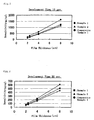
- Table-1 The results of Table-1 are shown as diagrams of each development times in Fig.-1 to Fig.-3 when putting film thickness in ⁇ m as horizontal axis and sensitivity in mJ/cm 2 as vertical axis.
- a thick film resist pattern which is used when manufacturing a semiconductor device, a magnetic head, a micro machine, etc. can be formed in higher sensitivity than the case using the radiation sensitive resin composition so far applied, without causing deterioration of film remaining ratio and with high resolution.
- the thick film resist pattern obtained by the present invention has no tailing and a good pattern shape.
- the radiation sensitive resin composition of the present invention can be applied for a photoresist for forming a resist pattern with thick film thickness and can be properly used for manufacturing semiconductor devices, a magnetic head, a micro machine, etc.
Landscapes
- Physics & Mathematics (AREA)
- Spectroscopy & Molecular Physics (AREA)
- General Physics & Mathematics (AREA)
- Materials For Photolithography (AREA)
- Exposure And Positioning Against Photoresist Photosensitive Materials (AREA)
Abstract
Description


| Eth in each condition (unit: mJ/cm2) | ||||
| Film thickness (µm) | | |||
| 10 | 30 | 60 sec | ||
| Example 1 | 2.0 | 154 | 63 | 34 |
| 2.4 | 214 | 87 | 47 | |
| 4.0 | 485 | 198 | 106 | |
| 8.0 | 1250 | 511 | 275 | |
| Example 2 | 2.0 | 142 | 56 | 30 |
| 2.4 | 198 | 78 | 43 | |
| 4.0 | 435 | 171 | 92 | |
| 8.0 | 1150 | 453 | 243 | |
| Comparative Example 1 | 2.0 | 205 | 72 | 38 |
| 2.4 | 322 | 115 | 64 | |
| 4.0 | 630 | 233 | 142 | |
| 8.0 | 1650 | 611 | 341 |
Claims (6)
- A method of forming a thick film resist pattern using a photoresist film having a film thickness of 2.0 µm or more, wherein a radiation sensitive resin composition comprises an alkali-soluble resin and a photosensitizer containing a quinone diazide group, and said alkali-soluble resin is a mixture of a novolak resin and one or more resins selected from the group consisting of (i) a polyacrylic ester, (ii) a polymethacrylic ester, (iii) a polystyrene derivative, and (iv) a copolymer comprising two or more monomer units selected from the group of an acrylic ester, a methacrylic ester and a styrene derivative.
- The method of forming a thick film resist pattern according to claim 1, wherein the photosensitizer containing a quinone diazide group is a mixture of two or more of esterified products having different esterification rate, which are produced by esterifying 1,2-naphthoquinone diazide sulfonic acid with tetrahydroxy benzophenone.
- The method of forming a thick film resist pattern according to claim 1 or 2, wherein the radiation sensitive resin composition contains a fluorescent material in an amount of 0.0001 to 1.0 part by weight relative to 100 parts by weight of the photosensitizer containing a quinone diazide group.
- A radiation sensitive resin composition for forming a thick film resist pattern comprising an alkali-soluble resin and a photosensitizer containing a quinone diazide group for use in the method of forming a thick film resist pattern according to claim 1, wherein said alkali-soluble resin is a mixture of a novolak resin and one or more resins selected from the group consisting of (i) a polyacrylic ester, (ii) a polymethacrylic ester, (iii) a polystyrene derivative, and (iv) a copolymer comprising two or more monomer units selected from the group of an acrylic ester, a methacrylic ester and a styrene derivative.
- The radiation sensitive resin composition for forming a thick film resist pattern according to claim 4, wherein the photosensitizer containing a quinone diazide group is a mixture of two or more of esterified products having different esterification rate, which are produced by esterifying 1,2-naphthoquinone diazide sulfonic acid with tetrahydroxy benzophenone.
- The radiation sensitive resin composition for forming a thick film resist pattern according to claim 4 or 5, which contains a fluorescent material in an amount of 0.0001 to 1.0 part by weight relative to 100 parts by weight of the photosensitizer containing a quinone diazide group.
Applications Claiming Priority (3)
| Application Number | Priority Date | Filing Date | Title |
|---|---|---|---|
| JP2001177561 | 2001-06-12 | ||
| JP2001177561A JP4213366B2 (en) | 2001-06-12 | 2001-06-12 | Method for forming thick film resist pattern |
| PCT/JP2002/005523 WO2002101467A1 (en) | 2001-06-12 | 2002-06-05 | Method of forming thick resist pattern |
Publications (2)
| Publication Number | Publication Date |
|---|---|
| EP1400850A1 true EP1400850A1 (en) | 2004-03-24 |
| EP1400850A4 EP1400850A4 (en) | 2006-06-07 |
Family
ID=19018387
Family Applications (1)
| Application Number | Title | Priority Date | Filing Date |
|---|---|---|---|
| EP02733301A Withdrawn EP1400850A4 (en) | 2001-06-12 | 2002-06-05 | Method of forming thick resist pattern |
Country Status (7)
| Country | Link |
|---|---|
| US (1) | US20040170917A1 (en) |
| EP (1) | EP1400850A4 (en) |
| JP (1) | JP4213366B2 (en) |
| KR (1) | KR100894802B1 (en) |
| CN (1) | CN1320406C (en) |
| TW (1) | TWI296354B (en) |
| WO (1) | WO2002101467A1 (en) |
Cited By (1)
| Publication number | Priority date | Publication date | Assignee | Title |
|---|---|---|---|---|
| US20130344249A1 (en) * | 2012-06-21 | 2013-12-26 | Jsr Corporation | Directed self-assembly composition for pattern formation and pattern-forming method |
Families Citing this family (14)
| Publication number | Priority date | Publication date | Assignee | Title |
|---|---|---|---|---|
| JP4101670B2 (en) | 2003-01-31 | 2008-06-18 | 東京応化工業株式会社 | Positive photoresist composition for LCD production and method for forming resist pattern |
| JP3842750B2 (en) * | 2003-03-25 | 2006-11-08 | Azエレクトロニックマテリアルズ株式会社 | Photosensitive resin composition |
| JP4440600B2 (en) * | 2003-10-31 | 2010-03-24 | Azエレクトロニックマテリアルズ株式会社 | Chemically amplified photosensitive resin composition for thick and ultra-thick films |
| JP4499591B2 (en) * | 2005-03-23 | 2010-07-07 | 東京応化工業株式会社 | Chemically amplified positive photoresist composition for thick film formation |
| JP2007053318A (en) * | 2005-08-19 | 2007-03-01 | Matsushita Electric Ind Co Ltd | Solid-state imaging device and manufacturing method thereof |
| TW200739265A (en) * | 2005-12-06 | 2007-10-16 | Tokyo Ohka Kogyo Co Ltd | Positive photoresist composition and method of forming photoresist pattern using the same |
| JP4813193B2 (en) * | 2006-01-31 | 2011-11-09 | Azエレクトロニックマテリアルズ株式会社 | Photosensitive resin composition suitable for spinless and slit coating |
| CN102393605B (en) * | 2006-12-27 | 2014-06-11 | 日立化成株式会社 | Photosensitive resin composition, photosensitive element, method for resist pattern formation, and method for manufacturing printed wiring board |
| TWI502031B (en) * | 2012-03-01 | 2015-10-01 | Eternal Materials Co Ltd | Anti-etching composition and its application |
| CN103357346B (en) * | 2013-06-27 | 2015-01-28 | 京东方科技集团股份有限公司 | Pigment dispersing agent, pigment dispersion liquid, colorized photoresist, and preparation and application thereof |
| KR102212674B1 (en) * | 2014-07-09 | 2021-02-05 | 동우 화인켐 주식회사 | Thick film pattern structure and Method for fabricating the same |
| WO2018029142A1 (en) * | 2016-08-09 | 2018-02-15 | AZ Electronic Materials (Luxembourg) S.à.r.l. | Enviromentally stable, thick film, chemically amplified resist |
| JP6702251B2 (en) * | 2017-04-17 | 2020-05-27 | 信越化学工業株式会社 | Positive resist film laminate and pattern forming method |
| CN107146774A (en) * | 2017-04-19 | 2017-09-08 | 深圳市环基实业有限公司 | A kind of IC package support plate and its packaging technology |
Family Cites Families (22)
| Publication number | Priority date | Publication date | Assignee | Title |
|---|---|---|---|---|
| US3666473A (en) * | 1970-10-06 | 1972-05-30 | Ibm | Positive photoresists for projection exposure |
| JPS5114042B2 (en) * | 1972-06-12 | 1976-05-06 | ||
| DE2236941C3 (en) | 1972-07-27 | 1982-03-25 | Hoechst Ag, 6000 Frankfurt | Photosensitive recording material |
| JPS5280022A (en) * | 1975-12-26 | 1977-07-05 | Fuji Photo Film Co Ltd | Light solubilizable composition |
| DE2847878A1 (en) * | 1978-11-04 | 1980-05-22 | Hoechst Ag | LIGHT SENSITIVE MIXTURE |
| DE3022473A1 (en) | 1980-06-14 | 1981-12-24 | Hoechst Ag, 6000 Frankfurt | LIGHT-SENSITIVE COPYING MATERIAL AND METHOD FOR THE PRODUCTION THEREOF |
| DE3442756A1 (en) * | 1984-11-23 | 1986-05-28 | Hoechst Ag, 6230 Frankfurt | RADIATION-SENSITIVE MIXTURE, RECORDING MATERIAL MADE THEREOF, AND METHOD FOR THE PRODUCTION OF HEAT-RESISTANT RELIEF RECORDINGS |
| JP2590342B2 (en) * | 1986-11-08 | 1997-03-12 | 住友化学工業株式会社 | Novolak resin for positive photoresist and positive photoresist composition containing the same |
| DE3827567A1 (en) * | 1988-08-13 | 1990-02-22 | Basf Ag | WAITER DEVELOPER SOLUTION FOR POSITIVELY WORKING PHOTORE RESTS |
| US5650261A (en) * | 1989-10-27 | 1997-07-22 | Rohm And Haas Company | Positive acting photoresist comprising a photoacid, a photobase and a film forming acid-hardening resin system |
| JP3424341B2 (en) * | 1994-04-11 | 2003-07-07 | 住友化学工業株式会社 | Photosensitive resin composition |
| US5561194A (en) * | 1995-03-29 | 1996-10-01 | International Business Machines Corporation | Photoresist composition including polyalkylmethacrylate co-polymer of polyhydroxystyrene |
| JPH08272089A (en) * | 1995-03-31 | 1996-10-18 | Toppan Printing Co Ltd | Positive photoresist composition and method for adjusting dissolution rate thereof |
| US5672459A (en) * | 1995-03-31 | 1997-09-30 | Japan Synthetic Rubber Co., Ltd. | Radiation sensitive resin composition containing quinone diazide ester having two hindered phenol groups |
| JP3784096B2 (en) * | 1995-12-19 | 2006-06-07 | ローム・アンド・ハース・エレクトロニック・マテリアルズ,エル.エル.シー. | Radiation sensitive coating composition and semiconductor manufacturing method using the same |
| US5641595A (en) * | 1996-01-16 | 1997-06-24 | Industrial Technology Research Institute | Manufacture of color filters by incremental exposure method |
| JP3633179B2 (en) * | 1997-01-27 | 2005-03-30 | Jsr株式会社 | Positive photoresist composition |
| EP1087260A4 (en) * | 1999-02-15 | 2002-01-16 | Clariant Finance Bvi Ltd | PHOTOSENSITIVE RESIN COMPOSITION |
| JP4204700B2 (en) * | 1999-06-08 | 2009-01-07 | Azエレクトロニックマテリアルズ株式会社 | Photosensitive resin composition and method for improving dry etching resistance of photosensitive resin composition |
| KR20010112227A (en) * | 1999-10-07 | 2001-12-20 | 데머 얀, 당코 제니아 떼. | Photosensitive composition |
| TW554250B (en) * | 2000-12-14 | 2003-09-21 | Clariant Int Ltd | Resist with high resolution to i ray and process for forming pattern |
| JP3710717B2 (en) * | 2001-03-06 | 2005-10-26 | 東京応化工業株式会社 | Positive photoresist composition for thick film, photoresist film, and bump forming method using the same |
-
2001
- 2001-06-12 JP JP2001177561A patent/JP4213366B2/en not_active Expired - Fee Related
-
2002
- 2002-05-16 TW TW091110220A patent/TWI296354B/en not_active IP Right Cessation
- 2002-06-05 EP EP02733301A patent/EP1400850A4/en not_active Withdrawn
- 2002-06-05 WO PCT/JP2002/005523 patent/WO2002101467A1/en not_active Ceased
- 2002-06-05 CN CNB028116186A patent/CN1320406C/en not_active Expired - Fee Related
- 2002-06-05 KR KR1020037016299A patent/KR100894802B1/en not_active Expired - Fee Related
- 2002-06-05 US US10/480,342 patent/US20040170917A1/en not_active Abandoned
Cited By (2)
| Publication number | Priority date | Publication date | Assignee | Title |
|---|---|---|---|---|
| US20130344249A1 (en) * | 2012-06-21 | 2013-12-26 | Jsr Corporation | Directed self-assembly composition for pattern formation and pattern-forming method |
| US9718950B2 (en) * | 2012-06-21 | 2017-08-01 | Jsr Corporation | Directed self-assembly composition for pattern formation and pattern-forming method |
Also Published As
| Publication number | Publication date |
|---|---|
| JP4213366B2 (en) | 2009-01-21 |
| US20040170917A1 (en) | 2004-09-02 |
| CN1320406C (en) | 2007-06-06 |
| KR100894802B1 (en) | 2009-04-24 |
| JP2002365799A (en) | 2002-12-18 |
| TWI296354B (en) | 2008-05-01 |
| EP1400850A4 (en) | 2006-06-07 |
| CN1518685A (en) | 2004-08-04 |
| KR20040030673A (en) | 2004-04-09 |
| WO2002101467A1 (en) | 2002-12-19 |
Similar Documents
| Publication | Publication Date | Title |
|---|---|---|
| US6475693B1 (en) | Positively photosensitive resin composition | |
| US6806019B2 (en) | High-resolution photosensitive resin composition usable with i-line and method of forming pattern | |
| JPH03155554A (en) | Radiation sensitive resin composition | |
| US20040170917A1 (en) | Method of forming thick resist pattern | |
| EP0539778B1 (en) | Positive type radiation-sensitive resist composition | |
| EP1143298A1 (en) | Photosensitive composition | |
| JPH03294861A (en) | Positive photoresist composition | |
| JPS62153950A (en) | Positive type radiation sensitive resin composition | |
| US6391513B1 (en) | Positively photosensitive resin composition | |
| JP2625883B2 (en) | Positive resist composition | |
| JP2536600B2 (en) | Method for removing low-nuclear body in novolak resin | |
| JP2629271B2 (en) | Composition for positive resist | |
| EP0416544B1 (en) | Radiation-sensitive positive resist composition | |
| EP0848291B1 (en) | Radiation-sensitive resin composition | |
| JPH09197667A (en) | Positive photo-resist composition | |
| JP3478378B2 (en) | Alkali-soluble novolak resin | |
| JP4312946B2 (en) | Photosensitive resin composition | |
| JP2000029209A (en) | Positive resist composition and method for producing the same | |
| JP4026220B2 (en) | Radiation sensitive resin composition | |
| JPH06138651A (en) | Negative radiation-sensitive resin composition | |
| JP2000075477A (en) | Positive resist composition | |
| JPH08328244A (en) | Positive photoresit composition | |
| JPH10133369A (en) | Radiation-sensitive resin composition | |
| JPWO2000034829A1 (en) | Positive photosensitive resin composition | |
| JPH11153862A (en) | Forming method of positive resist coating film |
Legal Events
| Date | Code | Title | Description |
|---|---|---|---|
| PUAI | Public reference made under article 153(3) epc to a published international application that has entered the european phase |
Free format text: ORIGINAL CODE: 0009012 |
|
| 17P | Request for examination filed |
Effective date: 20040112 |
|
| AK | Designated contracting states |
Kind code of ref document: A1 Designated state(s): AT BE CH CY DE DK ES FI FR GB GR IE IT LI LU MC NL PT SE TR |
|
| RAP1 | Party data changed (applicant data changed or rights of an application transferred) |
Owner name: CLARIANT FINANCE (BVI) LIMITED |
|
| RAP1 | Party data changed (applicant data changed or rights of an application transferred) |
Owner name: AZ ELECTRONIC MATERIALS USA CORP. |
|
| A4 | Supplementary search report drawn up and despatched |
Effective date: 20060425 |
|
| STAA | Information on the status of an ep patent application or granted ep patent |
Free format text: STATUS: THE APPLICATION IS DEEMED TO BE WITHDRAWN |
|
| 18D | Application deemed to be withdrawn |
Effective date: 20080102 |