EP1400804A1 - Method and device for measuring thermoelectric characteristics of combinatorial specimen - Google Patents
Method and device for measuring thermoelectric characteristics of combinatorial specimen Download PDFInfo
- Publication number
- EP1400804A1 EP1400804A1 EP02705181A EP02705181A EP1400804A1 EP 1400804 A1 EP1400804 A1 EP 1400804A1 EP 02705181 A EP02705181 A EP 02705181A EP 02705181 A EP02705181 A EP 02705181A EP 1400804 A1 EP1400804 A1 EP 1400804A1
- Authority
- EP
- European Patent Office
- Prior art keywords
- sample
- combinatorial
- measuring
- thermoelectric
- temperature gradient
- Prior art date
- Legal status (The legal status is an assumption and is not a legal conclusion. Google has not performed a legal analysis and makes no representation as to the accuracy of the status listed.)
- Granted
Links
Images


Classifications
-
- G—PHYSICS
- G01—MEASURING; TESTING
- G01K—MEASURING TEMPERATURE; MEASURING QUANTITY OF HEAT; THERMALLY-SENSITIVE ELEMENTS NOT OTHERWISE PROVIDED FOR
- G01K7/00—Measuring temperature based on the use of electric or magnetic elements directly sensitive to heat ; Power supply therefor, e.g. using thermoelectric elements
- G01K7/02—Measuring temperature based on the use of electric or magnetic elements directly sensitive to heat ; Power supply therefor, e.g. using thermoelectric elements using thermoelectric elements, e.g. thermocouples
-
- H—ELECTRICITY
- H10—SEMICONDUCTOR DEVICES; ELECTRIC SOLID-STATE DEVICES NOT OTHERWISE PROVIDED FOR
- H10N—ELECTRIC SOLID-STATE DEVICES NOT OTHERWISE PROVIDED FOR
- H10N10/00—Thermoelectric devices comprising a junction of dissimilar materials, i.e. devices exhibiting Seebeck or Peltier effects
-
- G—PHYSICS
- G01—MEASURING; TESTING
- G01R—MEASURING ELECTRIC VARIABLES; MEASURING MAGNETIC VARIABLES
- G01R31/00—Arrangements for testing electric properties; Arrangements for locating electric faults; Arrangements for electrical testing characterised by what is being tested not provided for elsewhere
- G01R31/26—Testing of individual semiconductor devices
Definitions
- the present invention relates to a method and device for measuring thermoelectric characteristics of a combinatorial sample.
- thermoelectric materials can be used for converting waste heat into electrical energy, electrical energy can be efficiently generated with conventional electric power-generating systems including such thermoelectric materials. Therefore, it is expected that new thermoelectric materials having higher efficiency are developed. Since a junction is cooled by the Peltier effect when a current is applied to a thermoelectric material, such a material is used for cooling systems. Therefore, demands have been made on new thermoelectric materials having higher efficiency.
- the following new semiconductors have been recently developed at a feverish pace: wide-gap semiconductors, transparent semiconductors, and organic semiconductors.
- Carrier control is the key to use such semiconductors for devices.
- Various devices such as transistors, FETs, diodes, and solar cells, laser oscillators can be manufactured using, for example, junctions (pn junctions) consisting of p-type semiconductors, in which the major carriers are holes, and n-type semiconductors, in which the major carriers are electrons. Therefore, the carrier type is particularly a critical property parameter.
- Carrier control is usually performed in such a manner that an undoped sample is subjected to impurity substitution or is heat-treated in an impurity gas atmosphere.
- the dose is very small, the control is not easy and therefore such treatment is performed by trial and error in many cases.
- the wide-gap semiconductors are treated, either a p type or an n type is apt to be obtained. Therefore, only either type has been fabricated and the conditions of fabrication are strictly limited. Thus, it is necessary to investigate more precise growing conditions and doping conditions.
- thermoelectric materials In the conventional investigation of thermoelectric materials, a large amount of time has been wasted because such materials are prepared one by one and the thermoelectric characteristics thereof are individually evaluated.
- thermoelectric characteristics is a critical factor and therefore it is necessary to continuously measure a large number of prepared minute samples at high speed.
- thermoelectric characteristics of a combinatorial sample wherein the method and device are useful for rapid sample evaluation, the investigation of thermoelectric materials, and the carrier control of semiconductors.
- the present invention provides the following method and device.
- hot baths is herein defined as portions of sample holders.
- the sample holders do not include simple (sample) holders but include holders having a certain heat capacity so as to maintain the temperature at a constant value during measurement (the holders are actually made of metal such as copper but are not made of, for example, plastic and so on having a small heat capacity).
- the holders are actually made of metal such as copper but are not made of, for example, plastic and so on having a small heat capacity.
- one hot bath is used.
- two hot baths must be used.
- the method for measuring thermoelectric characteristics of a combinatorial sample includes a step of applying a small temperature gradient to a combinatorial sample, patterned by a photolithographic process, to obtain a plurality of electrical signals from the combinatorial sample by wire-bonding.
- the device for measuring thermoelectric characteristics of a combinatorial sample includes a combinatorial sample patterned by a photolithographic process, a pair of sample holders for applying a small temperature gradient to the sample, a means for measuring the temperature gradient, and a wire-bonding means connected to the sample.
- FIG. 1 is a block diagram showing a combinatorial thermoelectric characteristic-measuring device, wherein the device is an example of the present invention.
- reference numeral 1 represents a sample stage
- reference numeral 2 represents a temperature controller
- reference numeral 3 represents a temperature difference controller
- reference numeral 4 represents a voltmeter
- reference numeral 5 represents an ammeter
- reference numeral 6 represents a line-switching unit
- reference numeral 7 represents a computer.
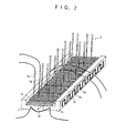
- FIG. 2 is a perspective view showing a measuring section of a combinatorial thermoelectric characteristic-measuring system, wherein the measuring section is a first example of the present invention.
- reference numeral 10 represents two-dimensional combinatorial samples (micro-samples) patterned using a metal mask
- reference numerals 11 and 12 represent a pair of sample holders for supporting the samples 10
- reference numeral 13 represents a heater disposed on the side of each sample holder
- reference numeral 14 represents a thermocouple disposed between a pair of the sample holders 11 and 12
- reference numeral 15 represents a probe pin array arranged so as to be uniformly in contact with a plurality of the combinatorial samples 10 arranged in a line.
- a small temperature gradient (for example, a gradient in which the temperature of one sample holder 12 is 3°C higher than that of the other sample holder 11) is applied to the samples 10, patterned using the metal mask, with the heater 13, and thereby a plurality of electrical signals can be obtained from the combinatorial samples 10 with the probe pin array 15 in contact with the samples 10.
- Combinatorial thermoelectric characteristics of the samples can be measured under the same conditions in one operation in such a manner that four probe pins 15a, 15b, 15c, and 15d are arranged in a line and a current is applied between the probe pins 15a and 15d to measure the potential difference between the probe pins 15b and 15c.
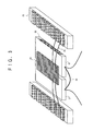
- FIG. 3 is a perspective view showing a measuring section of a combinatorial thermoelectric characteristic-measuring system, wherein the measuring section is a second example of the present invention.
- bonding wires for connection are used instead of the probe pin array of the first example.
- reference numeral 20 represents a two-dimensionally arranged combinatorial sample patterned by a photolithographic process
- reference numerals 21 and 22 represent a pair of sample holders for supporting the sample 20
- reference numeral 23 represents a heater disposed on the side of each sample holder
- reference numeral 24 represents a thermocouple disposed between a pair of the sample holders 21 and 22
- reference numeral 25 represents bonding terminals
- reference numeral 26 represents bonding wires disposed between the bonding terminals 25 and the sample 20.
- a small temperature gradient is applied to the sample 20, patterned by the photolithographic process, with the heater 23, and thereby a plurality of electrical signals can be obtained from the combinatorial sample 20 via the bonding terminal 25 by a wire bonding process using the bonding wires 26.
- FIG. 4 is a graph showing the thermoelectromotive force obtained with a device of the present invention.
- the vertical axis represents the temperature difference [ ⁇ T (°C)] and the horizontal axis represents the thermoelectromotive force ( ⁇ V).
- thermoelectromotive force varies linearly with the temperature difference.
- thermoelectric materials in a sample prepared by combinatorial thin film synthesis, a large number of data can be obtained from the measurement of the thermoelectromotive force and the electrical resistance. Thereby, high-speed screening is possible when thermoelectric materials are investigated.
- the device according to the present invention is an important factor in investigating thermoelectric materials.
- thermoelectric material-investigating technique The combinatorial thin-film synthesis using a mask system is a high-speed thermoelectric material-investigating technique and has sprung into wide use.
- thermoelectric materials When thermoelectric materials are investigated using this technique, it takes a long time to evaluate prepared thin-films, of which the thermoelectric characteristics are measured, because the thin-films are individually subjected to the measurement.
- thermoelectromotive force and electrical characteristics of thin-films prepared by the combinatorial synthesis can be simultaneously measured, thereby performing the high-speed evaluation of such electrical characteristics.
- the device can be used in various applications. For example, when carriers are introduced into semiconductors, the device can be used for readily determining whether the charge of the introduced carriers is positive or negative.
- two hot baths are used.
- two or more hot baths may be used.
- thermoelectromotive force and electrical characteristics of thin-films prepared by the combinatorial synthesis can be simultaneously measured, the high-speed evaluation of such electrical characteristics can be performed.
- the device according to the present invention is an important factor in investigating thermoelectric materials.
- the present invention can be used in various applications. For example, when carriers are introduced into semiconductors, the present invention can be used for readily determining whether the charge of the introduced carriers is positive or negative.
- thermoelectric characteristics of a combinatorial sample are important factors in investigating thermoelectric materials.
- the method and the device can be used in various applications. For example, when carriers are introduced into semiconductors, the method and the device can be used for readily determining whether the charge of the introduced carriers is positive or negative.
Landscapes
- Physics & Mathematics (AREA)
- General Physics & Mathematics (AREA)
- Investigating Or Analyzing Materials Using Thermal Means (AREA)
- Investigating Or Analyzing Materials By The Use Of Electric Means (AREA)
- Testing Or Measuring Of Semiconductors Or The Like (AREA)
Abstract
Description
Claims (2)
- A method for measuring thermoelectric characteristics of a combinatorial sample, comprising a step of applying a small temperature gradient to a patterned combinatorial sample disposed between two or more hot baths to obtain a plurality of electrical signals from the combinatorial sample.
- A device for measuring thermoelectric characteristics of a combinatorial sample, comprising:(a) a patterned combinatorial sample;(b) two or more hot baths for applying a small temperature gradient to the sample;(c) a means for measuring the temperature gradient; and(d) a component for obtaining a plurality of electrical signals in the temperature gradient direction, the component being in contact with or being connected to the sample.
Applications Claiming Priority (3)
| Application Number | Priority Date | Filing Date | Title |
|---|---|---|---|
| JP2001075954A JP3388731B2 (en) | 2001-03-16 | 2001-03-16 | Method and apparatus for measuring thermoelectric properties of combinatorial samples |
| JP2001075954 | 2001-03-16 | ||
| PCT/JP2002/002415 WO2002075297A1 (en) | 2001-03-16 | 2002-03-14 | Method and device for measuring thermoelectric characteristics of combinatorial specimen |
Publications (3)
| Publication Number | Publication Date |
|---|---|
| EP1400804A1 true EP1400804A1 (en) | 2004-03-24 |
| EP1400804A4 EP1400804A4 (en) | 2010-03-03 |
| EP1400804B1 EP1400804B1 (en) | 2016-01-13 |
Family
ID=18932962
Family Applications (1)
| Application Number | Title | Priority Date | Filing Date |
|---|---|---|---|
| EP02705181.2A Expired - Lifetime EP1400804B1 (en) | 2001-03-16 | 2002-03-14 | Method and device for measuring thermoelectric characteristics of combinatorial specimen |
Country Status (4)
| Country | Link |
|---|---|
| US (1) | US6902317B2 (en) |
| EP (1) | EP1400804B1 (en) |
| JP (1) | JP3388731B2 (en) |
| WO (1) | WO2002075297A1 (en) |
Families Citing this family (8)
| Publication number | Priority date | Publication date | Assignee | Title |
|---|---|---|---|---|
| JP4560628B2 (en) * | 2005-04-28 | 2010-10-13 | 国立大学法人東京工業大学 | Evaluation board for combinatorial materials |
| JP2007024603A (en) * | 2005-07-13 | 2007-02-01 | Toyota Motor Corp | Method for measuring thin film samples |
| CN1975448B (en) * | 2006-12-11 | 2010-08-11 | 中国科学院上海硅酸盐研究所 | Device and method for measuring performance of thermoelectric power generation components |
| US8087823B2 (en) * | 2008-08-18 | 2012-01-03 | International Business Machines Corporation | Method for monitoring thermal control |
| US9448121B2 (en) | 2012-04-10 | 2016-09-20 | Industrial Technology Research Institute | Measurement method, measurement apparatus, and computer program product |
| RU2646537C2 (en) * | 2015-11-30 | 2018-03-05 | Федеральное государственное бюджетное образовательное учреждение высшего профессионального образования "Тамбовский государственный технический университет" ФГБОУ ВПО ТГТУ | Coefficient of the thermoelectric power of materials measuring device |
| EP3340287B1 (en) * | 2016-12-23 | 2020-10-28 | Huawei Technologies Co., Ltd. | Pattern-based temperature measurement for a bonding device and a bonding system |
| CN115406929B (en) * | 2022-08-01 | 2025-11-11 | 中国科学院大连化学物理研究所 | Low-temperature thermal electric property characterization device in high-flux and high-precision material |
Family Cites Families (15)
| Publication number | Priority date | Publication date | Assignee | Title |
|---|---|---|---|---|
| US3733887A (en) * | 1972-01-31 | 1973-05-22 | Borg Warner | Method and apparatus for measuring the thermal conductivity and thermo-electric properties of solid materials |
| US4320344A (en) * | 1978-07-24 | 1982-03-16 | Nicholas William R | Metal-alloy thermoelectric characteristic analyzer |
| HU189716B (en) * | 1983-07-14 | 1986-07-28 | Budapesti Mueszaki Egyetem,Hu | Method and appaeatus for non-destructive testing the heat physical characteristics of materials |
| GB2233457A (en) * | 1989-06-21 | 1991-01-09 | Schlumberger Technologies Ltd | Temperature reference junction for a multichannel temperature sensing system. |
| JPH0518913A (en) * | 1991-07-10 | 1993-01-26 | Tokuyama Soda Co Ltd | Thermoelectromotive force measuring method and apparatus |
| JPH0552783A (en) * | 1991-08-28 | 1993-03-02 | Tokuyama Soda Co Ltd | Thermoelectric characteristic measuring device |
| JP2730662B2 (en) * | 1993-03-16 | 1998-03-25 | 株式会社ジャパンエナジー | Temperature measuring element and temperature measuring method |
| JPH06300719A (en) * | 1993-04-16 | 1994-10-28 | Tokuyama Soda Co Ltd | Method and apparatus for measuring thermoelectric conversion characteristic |
| JPH0755739A (en) * | 1993-08-20 | 1995-03-03 | Shinku Riko Kk | Thermoelectric property measuring method and device |
| JPH07324991A (en) * | 1994-06-02 | 1995-12-12 | Ohara Inc | Thermoelectric property measuring device |
| US5985356A (en) * | 1994-10-18 | 1999-11-16 | The Regents Of The University Of California | Combinatorial synthesis of novel materials |
| JPH09222403A (en) * | 1996-02-16 | 1997-08-26 | Hitachi Ltd | Physical property measurement device |
| DE19635264C1 (en) * | 1996-08-30 | 1998-04-16 | Max Planck Gesellschaft | Thermoelectric microprobe for thermomicroscopic measurement |
| EP1055121A1 (en) * | 1998-12-11 | 2000-11-29 | Symyx Technologies, Inc. | Sensor array-based system and method for rapid materials characterization |
| US6487515B1 (en) * | 2000-08-18 | 2002-11-26 | International Business Machines Corporation | Method and apparatus for measuring thermal and electrical properties of thermoelectric materials |
-
2001
- 2001-03-16 JP JP2001075954A patent/JP3388731B2/en not_active Expired - Fee Related
-
2002
- 2002-03-14 US US10/450,709 patent/US6902317B2/en not_active Expired - Lifetime
- 2002-03-14 EP EP02705181.2A patent/EP1400804B1/en not_active Expired - Lifetime
- 2002-03-14 WO PCT/JP2002/002415 patent/WO2002075297A1/en not_active Ceased
Also Published As
| Publication number | Publication date |
|---|---|
| EP1400804A4 (en) | 2010-03-03 |
| US20040047398A1 (en) | 2004-03-11 |
| WO2002075297A1 (en) | 2002-09-26 |
| JP2002277422A (en) | 2002-09-25 |
| US6902317B2 (en) | 2005-06-07 |
| EP1400804B1 (en) | 2016-01-13 |
| JP3388731B2 (en) | 2003-03-24 |
Similar Documents
| Publication | Publication Date | Title |
|---|---|---|
| US8101449B2 (en) | Process for altering thermoelectric properties of a material | |
| Liu et al. | Micro-thermoelectric generators based on through glass pillars with high output voltage enabled by large temperature difference | |
| Tainoff et al. | Network of thermoelectric nanogenerators for low power energy harvesting | |
| EP1400804B1 (en) | Method and device for measuring thermoelectric characteristics of combinatorial specimen | |
| US5982014A (en) | Microfabricated silicon thermopile sensor | |
| Adnane et al. | High temperature Hall measurement setup for thin film characterization | |
| Dzundza et al. | Development of high-precision hardware and software tools for automated determination of the characteristics of thermoelectric devices | |
| Mulla et al. | An easily constructed and inexpensive tool to evaluate the Seebeck coefficient | |
| Burkov et al. | Methods and apparatus for measuring thermopower and electrical conductivity of thermoelectric materials at high temperatures | |
| Smith | Temperature dependence of the work function of semiconductors | |
| Yoshino et al. | Low-dimensional organic conductors as thermoelectric materials | |
| Platzek et al. | Seebeck scanning microprobe for thermoelectric FGM | |
| Ziolkowski et al. | Application of high-throughput seebeck microprobe measurements on thermoelectric half-Heusler thin film combinatorial material libraries | |
| Webb | Measurement of thermal resistance using electrical methods | |
| Boulouz et al. | Fabrication of Thermoelectric Sensor and Cooling Devices Based on Elaborated Bismuth‐Telluride Alloy Thin Films | |
| Alessandrello et al. | Fabrication and low-temperature characterization of Si-implanted thermistors | |
| WO2005103646A1 (en) | Scanning probe microscope probe and production method therefor and scanning probe microscope and application method therefor and needle-like element and production method therefor and electron element and production method tehrefor and charge density wave quantum phase microscope and charge density wave quantum interferomet | |
| Ider et al. | A robust system for thermoelectric device characterization | |
| Salinas et al. | Probe Design for Thermopower Measurements Using a Differential Thermocouple | |
| Cronin et al. | Transport measurements of individual Bi nanowires | |
| RU2841289C1 (en) | Thermoelectric converter | |
| Ziolkowski et al. | Application overview of the potential Seebeck microscope | |
| Kempf | Novel Methods for Thermal and Thermoelectric Material Measurement and the Effect of Irradiation on Advanced Thermoelectric Materials | |
| Tainoff et al. | Thermoelectric nanogenerator networks: a viable source of power for autonomous wireless sensors | |
| Ghasemi | Investigating Flexible Microthermoelectric Generator Module for Ultra-Low-Power Medical System-On-A-Chip Application |
Legal Events
| Date | Code | Title | Description |
|---|---|---|---|
| PUAI | Public reference made under article 153(3) epc to a published international application that has entered the european phase |
Free format text: ORIGINAL CODE: 0009012 |
|
| 17P | Request for examination filed |
Effective date: 20030708 |
|
| AK | Designated contracting states |
Kind code of ref document: A1 Designated state(s): AT BE CH CY DE DK ES FI FR GB GR IE IT LI LU MC NL PT SE TR |
|
| AX | Request for extension of the european patent |
Extension state: AL LT LV MK RO SI |
|
| RAP1 | Party data changed (applicant data changed or rights of an application transferred) |
Owner name: JAPAN SCIENCE AND TECHNOLOGY AGENCY |
|
| RAP1 | Party data changed (applicant data changed or rights of an application transferred) |
Owner name: JAPAN SCIENCE AND TECHNOLOGY AGENCY |
|
| A4 | Supplementary search report drawn up and despatched |
Effective date: 20100203 |
|
| RIC1 | Information provided on ipc code assigned before grant |
Ipc: G01N 25/00 20060101ALI20100128BHEP Ipc: G01N 27/00 20060101AFI20021002BHEP |
|
| 17Q | First examination report despatched |
Effective date: 20100830 |
|
| GRAP | Despatch of communication of intention to grant a patent |
Free format text: ORIGINAL CODE: EPIDOSNIGR1 |
|
| INTG | Intention to grant announced |
Effective date: 20150917 |
|
| GRAS | Grant fee paid |
Free format text: ORIGINAL CODE: EPIDOSNIGR3 |
|
| GRAA | (expected) grant |
Free format text: ORIGINAL CODE: 0009210 |
|
| AK | Designated contracting states |
Kind code of ref document: B1 Designated state(s): DE FR GB |
|
| REG | Reference to a national code |
Ref country code: GB Ref legal event code: FG4D |
|
| REG | Reference to a national code |
Ref country code: FR Ref legal event code: PLFP Year of fee payment: 15 |
|
| REG | Reference to a national code |
Ref country code: DE Ref legal event code: R096 Ref document number: 60247736 Country of ref document: DE |
|
| REG | Reference to a national code |
Ref country code: DE Ref legal event code: R097 Ref document number: 60247736 Country of ref document: DE |
|
| PLBE | No opposition filed within time limit |
Free format text: ORIGINAL CODE: 0009261 |
|
| STAA | Information on the status of an ep patent application or granted ep patent |
Free format text: STATUS: NO OPPOSITION FILED WITHIN TIME LIMIT |
|
| 26N | No opposition filed |
Effective date: 20161014 |
|
| REG | Reference to a national code |
Ref country code: FR Ref legal event code: PLFP Year of fee payment: 16 |
|
| PGFP | Annual fee paid to national office [announced via postgrant information from national office to epo] |
Ref country code: FR Payment date: 20170210 Year of fee payment: 16 Ref country code: DE Payment date: 20170207 Year of fee payment: 16 |
|
| PGFP | Annual fee paid to national office [announced via postgrant information from national office to epo] |
Ref country code: GB Payment date: 20170208 Year of fee payment: 16 |
|
| REG | Reference to a national code |
Ref country code: DE Ref legal event code: R119 Ref document number: 60247736 Country of ref document: DE |
|
| GBPC | Gb: european patent ceased through non-payment of renewal fee |
Effective date: 20180314 |
|
| PG25 | Lapsed in a contracting state [announced via postgrant information from national office to epo] |
Ref country code: DE Free format text: LAPSE BECAUSE OF NON-PAYMENT OF DUE FEES Effective date: 20181002 |
|
| PG25 | Lapsed in a contracting state [announced via postgrant information from national office to epo] |
Ref country code: GB Free format text: LAPSE BECAUSE OF NON-PAYMENT OF DUE FEES Effective date: 20180314 |
|
| PG25 | Lapsed in a contracting state [announced via postgrant information from national office to epo] |
Ref country code: FR Free format text: LAPSE BECAUSE OF NON-PAYMENT OF DUE FEES Effective date: 20180331 |