EP1399896B1 - Cryptographic method of protecting an electronic chip against fraud - Google Patents
Cryptographic method of protecting an electronic chip against fraud Download PDFInfo
- Publication number
- EP1399896B1 EP1399896B1 EP02747515A EP02747515A EP1399896B1 EP 1399896 B1 EP1399896 B1 EP 1399896B1 EP 02747515 A EP02747515 A EP 02747515A EP 02747515 A EP02747515 A EP 02747515A EP 1399896 B1 EP1399896 B1 EP 1399896B1
- Authority
- EP
- European Patent Office
- Prior art keywords
- certificate
- chip
- bits
- output
- state
- Prior art date
- Legal status (The legal status is an assumption and is not a legal conclusion. Google has not performed a legal analysis and makes no representation as to the accuracy of the status listed.)
- Expired - Lifetime
Links
Images

Classifications
-
- G—PHYSICS
- G06—COMPUTING; CALCULATING OR COUNTING
- G06K—GRAPHICAL DATA READING; PRESENTATION OF DATA; RECORD CARRIERS; HANDLING RECORD CARRIERS
- G06K19/00—Record carriers for use with machines and with at least a part designed to carry digital markings
- G06K19/06—Record carriers for use with machines and with at least a part designed to carry digital markings characterised by the kind of the digital marking, e.g. shape, nature, code
- G06K19/067—Record carriers with conductive marks, printed circuits or semiconductor circuit elements, e.g. credit or identity cards also with resonating or responding marks without active components
- G06K19/07—Record carriers with conductive marks, printed circuits or semiconductor circuit elements, e.g. credit or identity cards also with resonating or responding marks without active components with integrated circuit chips
- G06K19/073—Special arrangements for circuits, e.g. for protecting identification code in memory
-
- G—PHYSICS
- G07—CHECKING-DEVICES
- G07F—COIN-FREED OR LIKE APPARATUS
- G07F7/00—Mechanisms actuated by objects other than coins to free or to actuate vending, hiring, coin or paper currency dispensing or refunding apparatus
- G07F7/08—Mechanisms actuated by objects other than coins to free or to actuate vending, hiring, coin or paper currency dispensing or refunding apparatus by coded identity card or credit card or other personal identification means
- G07F7/10—Mechanisms actuated by objects other than coins to free or to actuate vending, hiring, coin or paper currency dispensing or refunding apparatus by coded identity card or credit card or other personal identification means together with a coded signal, e.g. in the form of personal identification information, like personal identification number [PIN] or biometric data
- G07F7/1008—Active credit-cards provided with means to personalise their use, e.g. with PIN-introduction/comparison system
-
- G—PHYSICS
- G06—COMPUTING; CALCULATING OR COUNTING
- G06Q—INFORMATION AND COMMUNICATION TECHNOLOGY [ICT] SPECIALLY ADAPTED FOR ADMINISTRATIVE, COMMERCIAL, FINANCIAL, MANAGERIAL OR SUPERVISORY PURPOSES; SYSTEMS OR METHODS SPECIALLY ADAPTED FOR ADMINISTRATIVE, COMMERCIAL, FINANCIAL, MANAGERIAL OR SUPERVISORY PURPOSES, NOT OTHERWISE PROVIDED FOR
- G06Q20/00—Payment architectures, schemes or protocols
- G06Q20/30—Payment architectures, schemes or protocols characterised by the use of specific devices or networks
- G06Q20/34—Payment architectures, schemes or protocols characterised by the use of specific devices or networks using cards, e.g. integrated circuit [IC] cards or magnetic cards
- G06Q20/341—Active cards, i.e. cards including their own processing means, e.g. including an IC or chip
-
- G—PHYSICS
- G06—COMPUTING; CALCULATING OR COUNTING
- G06Q—INFORMATION AND COMMUNICATION TECHNOLOGY [ICT] SPECIALLY ADAPTED FOR ADMINISTRATIVE, COMMERCIAL, FINANCIAL, MANAGERIAL OR SUPERVISORY PURPOSES; SYSTEMS OR METHODS SPECIALLY ADAPTED FOR ADMINISTRATIVE, COMMERCIAL, FINANCIAL, MANAGERIAL OR SUPERVISORY PURPOSES, NOT OTHERWISE PROVIDED FOR
- G06Q20/00—Payment architectures, schemes or protocols
- G06Q20/38—Payment protocols; Details thereof
- G06Q20/40—Authorisation, e.g. identification of payer or payee, verification of customer or shop credentials; Review and approval of payers, e.g. check credit lines or negative lists
- G06Q20/409—Device specific authentication in transaction processing
- G06Q20/4097—Device specific authentication in transaction processing using mutual authentication between devices and transaction partners
- G06Q20/40975—Device specific authentication in transaction processing using mutual authentication between devices and transaction partners using encryption therefor
-
- G—PHYSICS
- G09—EDUCATION; CRYPTOGRAPHY; DISPLAY; ADVERTISING; SEALS
- G09C—CIPHERING OR DECIPHERING APPARATUS FOR CRYPTOGRAPHIC OR OTHER PURPOSES INVOLVING THE NEED FOR SECRECY
- G09C1/00—Apparatus or methods whereby a given sequence of signs, e.g. an intelligible text, is transformed into an unintelligible sequence of signs by transposing the signs or groups of signs or by replacing them by others according to a predetermined system
-
- H—ELECTRICITY
- H04—ELECTRIC COMMUNICATION TECHNIQUE
- H04L—TRANSMISSION OF DIGITAL INFORMATION, e.g. TELEGRAPHIC COMMUNICATION
- H04L9/00—Cryptographic mechanisms or cryptographic arrangements for secret or secure communications; Network security protocols
- H04L9/32—Cryptographic mechanisms or cryptographic arrangements for secret or secure communications; Network security protocols including means for verifying the identity or authority of a user of the system or for message authentication, e.g. authorization, entity authentication, data integrity or data verification, non-repudiation, key authentication or verification of credentials
- H04L9/3263—Cryptographic mechanisms or cryptographic arrangements for secret or secure communications; Network security protocols including means for verifying the identity or authority of a user of the system or for message authentication, e.g. authorization, entity authentication, data integrity or data verification, non-repudiation, key authentication or verification of credentials involving certificates, e.g. public key certificate [PKC] or attribute certificate [AC]; Public key infrastructure [PKI] arrangements
-
- H—ELECTRICITY
- H04—ELECTRIC COMMUNICATION TECHNIQUE
- H04L—TRANSMISSION OF DIGITAL INFORMATION, e.g. TELEGRAPHIC COMMUNICATION
- H04L2209/00—Additional information or applications relating to cryptographic mechanisms or cryptographic arrangements for secret or secure communication H04L9/00
- H04L2209/56—Financial cryptography, e.g. electronic payment or e-cash
Definitions
- the present invention relates to the field of cryptography.
- the invention relates to a cryptographic method of protection against fraud of an electronic chip in transactions between an application and the chip.
- the invention furthermore relates to an electronic chip device enabling the setting implementation of a cryptographic method of protection against chip fraud electronic.
- the invention finds a very advantageous application in that it makes it possible to protect against the fraud of wired logic integrated circuit chips or microprocessor, including the chips that equip the prepaid cards used in miscellaneous transactions such as the establishment of telephone calls, the payment of objects in a vending machine, the rental of Parking from a parking meter, payment for a service such as a transport public or as the provision of infrastructure (toll, museum, library,).
- a first type of fraud consists in duplicating without authorization the card, the term cloning is often used to characterize this operation.
- a second type fraud is to modify the data attached to a card, in particular the amount of credit entered in the card.
- Cryptography involves two entities, one checker and an object to check, and it can be either symmetrical or asymmetrical. When symmetrical, the two entities share exactly the same information, especially a secret key.
- the first authentication mechanisms developed in cryptography symmetrical approach consists in calculating once and for all a certificate, different for each card, to store it in the memory of the card, to read it at each transaction and to check it by querying a network application supporting the transaction where the already assigned certificates are either stored or recalculated. These mechanisms ensure Insufficient protection because the certificate can be spied on, reproduced and replayed fraudulently since it is always the same for a given card, thus making it possible to make a clone of this card. To fight against clones, Passive authentication mechanisms of cards are replaced by mechanisms Active authentication that can further ensure the integrity of the data.
- the general principle of active authentication mechanisms is as follows: authentication, the microchip and the application calculate a certificate that is the result of a function applied to a list of arguments determined at each authentication; the list of arguments that may include a hazard, the hazard being a data determined by the application at each authentication, a piece of data in the microchip and a secret key known to the microchip and to the application.
- the certificate calculated by the microchip is identical to the certificate calculated by the application, the microchip is deemed authentic and the transaction between the microchip and the application is allowed.
- the present invention relates to the mechanisms symmetric and active authentication methods that can be implemented in a card wired logic.
- a first of these mechanisms is the subject of patent FR 89 09734.
- the process described is to define a nonlinear function, this function being known from application and implanted in an electronic chip in the form of a wired circuit.
- a second of these mechanisms is the subject of patent FR 95 12144. This is a method card protection with unconditionally secure active authentication, based on the use for a limited number of authentications of a linear function ensuring protection against replay and controlled wear of the secret key.
- patent FR 89 09734 discloses a wired microcircuit card. in which a serial cryptographic function is applied to two operands, whose one is a "keyword” (for example a random R provided by an entity external to the card) and the other is an "output" of the "internal memory” of the card (eg a key secret K or data D related to the application).
- the serial cryptographic function is performed by a wired circuit comprising a logic operator receiving said keyword and said output of said internal memory, followed by a delay logic circuit having delay means and forming a loop between the outputs and the address inputs of a secret memory. The output of the logical operator intervenes on the data outputs secret memory to make up the new address entries of this secret memory.
- This method has several disadvantages.
- a first disadvantage comes from the fact that the keyword and the output of the memory are combined according to a simple logical operator. More precisely, the bits of keyword are used successively to constitute the first operand of the operator logic and the bits of the output of the internal memory are used successively for constitute the second operand of this operator. Therefore the intervention of a bit given the keyword or a given bit of the output of the internal memory on the circuit delay logic is limited exclusively to the moment when it is presented as input to the logical operator.
- a second disadvantage comes from the fact that the logical operator of the wired circuit has as input argument the keyword and the output of the internal memory which forbids to the logical operator to be able to combine the output of an internal memory with the output from another internal memory. For example, a secret key and a given registered in the chip can not be combined by this operator logic. It follows that the fraudulent modification of application data could find it easier.
- the use of a delay logic circuit forming a loop between data output and memory address entries are very restrictive. it excludes in particular that the output of the wired circuit is of length (expressed in bits) very high because the memory size increases exponentially with this length. For example, if the output has a length of 4 bits, then the memory occupies 64 bits. But if the output has a length of 8 bits, then the memory occupies 2 Kbit, size very high for a low cost logic chip. If the output has a length of 16 bits, so the memory occupies 1Mbit, size too high for any chip to wired logic. However, the length of the output of the wired circuit must be of length such as a fraudster who would try to guess the value at random has only one chance negligible to succeed.
- Patent application FR 2 739 706 describes a cryptographic process of protection against the fraud of an electronic chip. This process consists of calculating the chip a certificate from input parameters, to perform the state change of a finite state machine by changing it from an old state to a state new state according to a function depending at least on the old state and a value of input parameters, to calculate the certificate by means of an output function having for input argument at least one state of the automaton.
- the present invention relates to a cryptographic protection method against the fraud of an electronic chip and an electronic chip device, in transactions between an application and the microchip, specifically adapted to wired logic chips and more particularly intended to set up an authentication mechanism, which has no disadvantages mentioned above, in order to enhance the cryptographic robustness of the mechanism obtained authentication, and thus make the creation of clones more difficult.
- Process and device input parameters can, in the case of the implementation of an authentication mechanism, be consisting of a secret key K, a randomness R, application data D, an address A, an identifier I, etc.
- the input parameters of the cryptographic process and the device are processed in the mix function that outputs a data dependent on everything or part of the input parameters.
- the output data of the mixing function comes into play in the state change of the finite state machine, including at least one state, preferentially the final state, is used to calculate the output value, called certificate S.
- the automaton makes it possible to obtain size certificates high (16, 32 or even 64 bits) without having to store a large number of bits.
- the automaton does not necessarily consist of a simple logic circuit delay loop between the data outputs and the address inputs of a memory.
- the certificate obtained by implementing a method and a device according to the invention can be used both to exchange secret keys between the application and the chip, or encrypt data exchanged between the application and the chip, only for authentication of the chip or application. It can also be interpreted as an electronic signature of all or part of the input parameters. It can still be interpreted as a sequence of pseudo-random bits and, in varying at least one of the input parameters, the method of calculating the certificate then becomes a method of generating pseudo-random bits.
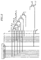
- FIG. 1 schematically represents a method according to the invention of protection of an electronic chip against fraud.
- the process consists of different functions described below.
- Each input parameter E m comprises a certain number of bits.
- the input data of the mixing function consist of all or part of the input parameters E m .
- a first input parameter E may consist of a secret key K, stored in a protected area of the chip, that is to say in a memory area of the that it is not possible to read or modify from the outside.
- This memory area can for example be implanted in a register or in a memory.
- a second input parameter E 2 may consist of data D internal to the chip, that is to say stored in a programmable memory (RAM, PROM, EPROM or E2PROM type) of the chip.
- RAM programmable memory
- PROM programmable read-only memory
- E2PROM programmable read-only memory
- These data can be of very different natures, and can be written during very different phases of the life of the chip, such as the manufacturing phase of the chip, the manufacturing phase of the object (card, ticket, etc.). ) in which the chip is inserted, the personalization phase of this object by the issuing entity, or the phase of use of the object by its holder.
- a third input parameter E 3 may, in the case where an input parameter consists of data D internal to the card, consist of the address or addresses of the memory area (s) of the chip in which this data D is stored.
- a fourth input parameter E 4 may consist of data D 'external to the chip, provided to the chip prior to the implementation of the cryptographic method, for example at the beginning of the transaction with the application.
- a fifth input parameter E 5 may consist of a random R external to the chip, provided to the chip prior to the implementation of the cryptographic method for example at the beginning of the transaction with the application.
- This hazard can be a random value, that is to say randomly chosen, of sufficiently large size that the probability of choosing two equal values is very low. It can also be determined from a sequence of consecutive integers generated by the application and the microchip. It can still be determined from time characteristics, typically the date and time. Finally, it can be a combination of all or part of the aforementioned elements.
- a sixth input parameter E 6 may consist of an internal chip hazard R 'supplied to the chip prior to the implementation of the cryptographic method.
- This hazard can be determined from a random value, that is to say randomly chosen, and of sufficiently large size that the probability of choosing two equal values is very low. It can also be determined from a sequence of consecutive integers generated by the outside, typically the application, and the electronic chip. It can still be determined from time characteristics, typically the date and time. Finally, it can be a combination of all or part of the aforementioned elements.
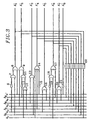
- the mixing function can be a linear or non-linear function of input data.
- Each door 5 j , j +1 exclusive OR has two inputs and one output. At least one input is the output of an AND logic j 4, the second input is the output of a gate 5, j + 1 XOR, or the output of an AND logic 4 j.
- the output e 'of the exclusive gate 5 J -1, J OR gives the value of the first bit of the output data of the MIX function.
- a rotation operation of one or more positions, is performed on the key K.
- This operation transforms the key K into a data item K '.
- the second bit of the output data of the mixing function can be defined as the dot product of the data K 'and the set of J bits (Z 1 , Z 2 , ... Z J ).
- the second bit is present at the output e 'of the gate 5 J -1, J OR exclusive.
- the linear function 1 thus defined.
- I is the desired number of output bits
- K key of I + J bits (K 1 , K 2 , ..., K I + J ).
- the first bit of the output data of the mixing function can be defined as the dot product of the data (K 1 , K 2 , ..., K J ) and (Z 1 , Z 2 , ... Z J ).
- the second bit of the output data can be defined as the scalar product of the data (K 2 , K 3 , ..., K J + 1 ) and (Z 1 , Z 2 , ... Z J ). And so on until the last bit of the output data which can be defined as the scalar product of the vectors (K I + 1 , K I + 2 , ..., K J + 1 ) and (Z 1 , Z 2 , ... Z J ).
- This variant is advantageous in that there is an implementation mode that dispenses to re-read the key K each time an output bit is required.
- a second example of a linear function 1 is to use a register to linear feedback offset in which input parameter bits are entered successively and affect the initial state of the register and / or the value of the bits of feedback.
- the term disturbed linear feedback shift register is sometimes used to designate a register in which data is injected in the course of operation of the register.
- the output value E 'can then consist of one or several bits extracted from the contents of this register.
- An example of a non-linear function 1 is to use a register to non-linear feedback offset, in which the bits of the input parameters are entered successively.
- the output value S ' may consist of one or more bits extracts from the contents of this register.
- a second function 2 consists in performing the state change of a finite state machine by changing it from an old state to a new state taking into account at least the old state and a value of the bit sequence.
- E ' ( e ' / 1, e '/ 2, ... e ' / n , ..., e '/ N ), which value corresponds to a bit or to several bits taken from the set of the data E '.
- this function can also take into account all or part of the input parameters E m .
- the initial state of the automaton can be determined according to all or part of E 'and E m .
- the automaton has an internal state of k bits (A 1 , A 2 , ... A k ) and presents at the output a new state (A ' 1 , A' 2 , ... A ' k ), whenever a new vector (A 1 , A 2 , ... A k , e ') is present at the input of the Boolean circuit, the new vector consisting of the internal state and the output of the mixing function.
- the transformation T is defined by a table that associates with each quartet value (a, b, c, d) a quartet value (a ', b', c ', d'). Similarly for U.
- the automaton is in a certain final state (F 1 , F 2 , ... F k ).
- a third function 3, called output, having as input arguments at least one state of the automaton, consists in calculating a certificate S.
- the simplest implementation is obtained by taking into account only the final state of the system. PLC.
- the function can take into account in a complementary manner the previous states of the automaton.
- the output function is the identity function applied to the final state of the automaton.
- the certificate S is equal to the data of k bits (F 1 , F 2 , ... F k ).
- the output function is a truncation function.
- the certificate S can be verified by any application having knowledge of the secret key K of the chip.
- all the data unknown to the application but included in the calculation of the certificate must be communicated by the chip to the application, previously, simultaneously or after the sending of the certificate.
- the application implements exactly the same cryptographic method as that implemented by the chip using the same input data as those used by the chip, and obtains a certificate S '.
- the application compares the certificate S 'which it has calculated with that S calculated by the chip. If there is a tie, the chip is considered authentic by the application.
- the verification of the certificate calculated by the application may be performed by the chip to enable the latter to authenticate the application.
- FIG. 4 illustrates the implementation of a method according to the invention, during a transaction between an electronic chip and an application.
- the electronic chip is hosted by a support 24 which consists of example in a prepaid card, in an electronic ticket, in a bank card, etc.
- the application 25 proceeds in whole or in part in a chip reader 26 electronic.
- This reader can be a contactless reader or a reader with contact as shown in Figure 4.
- the application When the application consists of an authentication application, the only presence of the card in the reader can activate this player and trigger the application.
- the application requests the chip for the latter to authenticate itself by providing it with a S certificate calculated 27 according to a method according to the invention.
- the application calculates 28 by the same method a certificate from the same input parameters than the chip.
- the chip At the end of the calculation, the chip provides its result to the application that the compare with his own result.
- the authentication of the chip is correct and the application informs the chip.
- the input parameters can be determined definitively before any use of the electronic chip implanted in the chip and known to the application. They can possibly be updated after authentication of the card according to a determined process. The update may concern all the parameters or only some of them or even the app can provide a new parameter as a hazard R determined randomly or determined by the value a counter, a clock, a date, etc ...
Abstract
Description
La présente invention se rapporte au domaine de la cryptographie. En particulier, l'invention se rapporte à un procédé cryptographique de protection contre la fraude d'une puce électronique dans des transactions entre une application et la puce. L'invention se rapporte en outre à un dispositif à puce électronique permettant la mise en oeuvre d'un procédé cryptographique de protection contre la fraude de la puce électronique.The present invention relates to the field of cryptography. In particular, the invention relates to a cryptographic method of protection against fraud of an electronic chip in transactions between an application and the chip. The invention furthermore relates to an electronic chip device enabling the setting implementation of a cryptographic method of protection against chip fraud electronic.
L'invention trouve une application très avantageuse en ce qu'elle permet de protéger contre la fraude des puces à circuit intégré à logique câblée ou à microprocesseur, notamment les puces qui équipent les cartes prépayées utilisées dans des transactions diverses telles que l'établissement de communications téléphoniques, le paiement d'objets dans un distributeur automatique, la location d'emplacements de stationnement à partir d'un parcmètre, le paiement d'un service comme un transport public ou comme la mise à disposition d'infrastructures (péage, musée, bibliothèque,...).The invention finds a very advantageous application in that it makes it possible to protect against the fraud of wired logic integrated circuit chips or microprocessor, including the chips that equip the prepaid cards used in miscellaneous transactions such as the establishment of telephone calls, the payment of objects in a vending machine, the rental of Parking from a parking meter, payment for a service such as a transport public or as the provision of infrastructure (toll, museum, library,...).
Actuellement, les cartes prépayées sont susceptibles de subir différents types de fraude. Un premier type de fraude consiste à dupliquer sans autorisation la carte, le terme clonage étant souvent utilisé pour caractériser cette opération. Un deuxième type de fraude consiste à modifier les données attachées à une carte, en particulier le montant du crédit inscrit dans la carte. Pour lutter contre ces fraudes il est fait appel à la cryptographie, d'une part pour assurer l'authentification de la carte au moyen d'une authentification et/ou pour assurer l'authentification des données au moyen d'une signature numérique et, d'autre part pour assurer le cas échéant la confidentialité des données au moyen d'un chiffrement. La cryptographie met en jeu deux entités, un vérificateur et un objet à vérifier, et elle peut être soit symétrique, soit asymétrique. Lorsqu'elle est symétrique, les deux entités partagent exactement la même information, en particulier une clé secrète. Lorsqu'elle est asymétrique une des deux entités possède une paire de clés dont l'une est secrète et l'autre est publique ; il n'y a pas de clé secrète partagée. Dans de nombreux systèmes, seule la cryptographie symétrique est mise en oeuvre avec des cartes prépayées, car la cryptographie asymétrique reste lente et coûteuse. Les premiers mécanismes d'authentification développés en cryptographie symétrique consistent à calculer une fois pour toutes un certificat, différent pour chaque carte, à le stocker dans la mémoire de la carte, à le lire à chaque transaction et à le vérifier en interrogeant une application du réseau supportant la transaction où les certificats déjà attribués sont soit stockés soit recalculés. Ces mécanismes assurent une protection insuffisante parce que le certificat peut être espionné, reproduit et rejoué frauduleusement étant donné qu'il est toujours le même pour une carte donnée, permettant ainsi de réaliser un clone de cette carte. Pour lutter contre les clones, les mécanismes d'authentification passifs de cartes sont remplacés par des mécanismes d'authentification actifs qui peuvent en outre assurer l'intégrité des données.Currently, prepaid cards are likely to experience different types of fraud. A first type of fraud consists in duplicating without authorization the card, the term cloning is often used to characterize this operation. A second type fraud is to modify the data attached to a card, in particular the amount of credit entered in the card. To fight against these frauds it is appealed to cryptography, on the one hand to ensure the authentication of the card by means of a authentication and / or to authenticate the data by means of a digital signature and, on the other hand, to ensure, where appropriate, the confidentiality of data by means of encryption. Cryptography involves two entities, one checker and an object to check, and it can be either symmetrical or asymmetrical. When symmetrical, the two entities share exactly the same information, especially a secret key. When asymmetric one of the two entities has a pair of keys, one of which is secret and the other is public; there is no key secret shared. In many systems, only symmetric cryptography is implementation with prepaid cards, because asymmetric cryptography remains slow and expensive. The first authentication mechanisms developed in cryptography symmetrical approach consists in calculating once and for all a certificate, different for each card, to store it in the memory of the card, to read it at each transaction and to check it by querying a network application supporting the transaction where the already assigned certificates are either stored or recalculated. These mechanisms ensure Insufficient protection because the certificate can be spied on, reproduced and replayed fraudulently since it is always the same for a given card, thus making it possible to make a clone of this card. To fight against clones, Passive authentication mechanisms of cards are replaced by mechanisms Active authentication that can further ensure the integrity of the data.
Le principe général des mécanismes d'authentification actifs est le suivant : lors d'une authentification, la puce électronique et l'application calculent un certificat qui est le résultat d'une fonction appliquée à une liste d'arguments déterminée à chaque authentification ; la liste d'arguments pouvant comprendre un aléa, l'aléa étant une donnée déterminée par l'application à chaque authentification, une donnée contenue dans la puce électronique et une clé secrète connue de la puce électronique et de l'application. Lorsque le certificat calculé par la puce électronique est identique au certificat calculé par l'application, la puce électronique est jugée authentique et la transaction entre la puce électronique et l'application est autorisée.The general principle of active authentication mechanisms is as follows: authentication, the microchip and the application calculate a certificate that is the result of a function applied to a list of arguments determined at each authentication; the list of arguments that may include a hazard, the hazard being a data determined by the application at each authentication, a piece of data in the microchip and a secret key known to the microchip and to the application. When the certificate calculated by the microchip is identical to the certificate calculated by the application, the microchip is deemed authentic and the transaction between the microchip and the application is allowed.
De tels mécanismes d'authentification sont largement connus mais la plupart exigent des capacités de calcul au moins égales à celles dont dispose un microprocesseur. Ces mécanismes conviennent donc aux cartes à microprocesseur, mais rarement aux cartes à logique câblée, lesquelles disposent de moyens de calcul beaucoup plus rudimentaires. La présente invention se rapporte aux mécanismes d'authentification symétriques et actifs qui peuvent être mis en oeuvre dans une carte à logique câblée.Such authentication mechanisms are widely known but most require computing capacities at least equal to those available to a microprocessor. These mechanisms are therefore suitable for microprocessor cards, but rarely to hard-wired logic cards, which have means of calculation much more rudimentary. The present invention relates to the mechanisms symmetric and active authentication methods that can be implemented in a card wired logic.
Un premier de ces mécanismes fait l'objet du brevet FR 89 09734. Le procédé décrit consiste à définir une fonction non linéaire, cette fonction étant connue de l'application et implantée dans une puce électronique sous la forme d'un circuit câblé. Un second de ces mécanismes fait l'objet du brevet FR 95 12144. Il s'agit d'un procédé de protection des cartes par authentification active inconditionnellement sûre, basé sur l'utilisation pour un nombre limité d'authentifications d'une fonction linéaire assurant une protection contre le rejeu et une usure contrôlée de la clé secrète.A first of these mechanisms is the subject of patent FR 89 09734. The process described is to define a nonlinear function, this function being known from application and implanted in an electronic chip in the form of a wired circuit. A second of these mechanisms is the subject of patent FR 95 12144. This is a method card protection with unconditionally secure active authentication, based on the use for a limited number of authentications of a linear function ensuring protection against replay and controlled wear of the secret key.
Chacun des deux mécanismes précédemment cités possède des avantages et des inconvénients spécifiques. En ce qui concerne le premier mécanisme, qui repose sur l'hypothèse (non prouvable dans l'état actuel des connaissances) de la sécurité informatique de la fonction non linéaire utilisée, les très fortes contraintes imposées par les capacités de calculs réduites des puces à logique câblée n'autorisent pas une marge de sécurité aussi large que pour les algorithmes à clé secrète usuels et, de ce fait la divulgation de la spécification détaillée de la fonction non linéaire utilisée peut représenter un risque. En ce qui concerne le second mécanisme, il possède l'avantage de bénéficier d'une sécurité prouvable tant que le nombre d'authentifications n'excède pas un certain seuil, et il n'y a donc pas de risque lié à la divulgation de la fonction linéaire utilisée mais, par contre la nécessité de limiter strictement le nombre d'utilisations de la fonction d'authentification pour la durée de vie de la puce (ou dans le cas de cartes rechargeables, entre deux rechargements) inhérente à cette solution peut représenter une contrainte difficile à satisfaire pour certaines applications. En outre, des attaques portant non pas sur les puces à logique câblée mais, sur les modules de sécurité utilisés pour la vérification de ces puces et, selon lesquelles un fraudeur fournirait à des modules de vérification des réponses aléatoires jusqu'à ce qu'un nombre suffisant de bonnes réponses, obtenues par hasard, lui fournisse le secret associé à un numéro de carte de son choix, peuvent être plus difficiles à contrer dans le cas du second mécanisme. Des combinaisons de ces deux types de mécanismes permettant de cumuler leurs avantages ont fait l'objet des brevets FR 00 03684 et FR 0004313.Each of the two mechanisms mentioned above has advantages and specific disadvantages. With regard to the first mechanism, which is based on the hypothesis (not provable in the current state of knowledge) of the security computing the non-linear function used, the very strong constraints imposed by the reduced computation capabilities of wired logic chips do not allow a margin of safety as wide as for the usual secret key algorithms and, as a result, the disclosure of the detailed specification of the non-linear function used may represent a risk. Regarding the second mechanism, he has the advantage to have provable security as long as the number of authentications does not exceed not a certain threshold, and so there is no risk related to the disclosure of the function used but, on the other hand, the need to strictly limit the number of uses of the authentication function for the lifetime of the chip (or in the case of reloadable cards, between two reloads) inherent to this solution can represent a constraint difficult to satisfy for certain applications. In addition, attacks not on wired logic chips but, on the modules used for the verification of these chips and, according to which a fraudster provide verification modules with random responses until a sufficient number of good answers, obtained by chance, provide him with the secret associated with a card number of one's choice, may be more difficult to counter in the case of the second mechanism. Combinations of these two types of mechanisms to cumulate their advantages have been the subject of patents FR 00 03684 and FR 0004313.
Plus précisément, le brevet FR 89 09734 décrit une carte à microcircuit câblé dans laquelle une fonction cryptographique série est appliquée à deux opérandes, dont l'un est un « mot-clé » (par exemple un aléa R fourni par une entité externe à la carte) et l'autre est une « sortie » de la « mémoire interne » de la carte (par exemple une clé secrète K ou une donnée D liée à l'application). La fonction cryptographique série est réalisée par un circuit câblé comprenant un opérateur logique recevant ledit mot-clé et ladite sortie de ladite mémoire interne, suivi d'un circuit logique à retard possédant des moyens à retard et formant boucle entre les sorties et les entrées d'adresses d'une mémoire secrète. La sortie de l'opérateur logique intervient sur les sorties de données de la mémoire secrète pour constituer les nouvelles entrées d'adresses de cette mémoire secrète.More specifically, patent FR 89 09734 discloses a wired microcircuit card. in which a serial cryptographic function is applied to two operands, whose one is a "keyword" (for example a random R provided by an entity external to the card) and the other is an "output" of the "internal memory" of the card (eg a key secret K or data D related to the application). The serial cryptographic function is performed by a wired circuit comprising a logic operator receiving said keyword and said output of said internal memory, followed by a delay logic circuit having delay means and forming a loop between the outputs and the address inputs of a secret memory. The output of the logical operator intervenes on the data outputs secret memory to make up the new address entries of this secret memory.
Ce procédé présente plusieurs inconvénients.This method has several disadvantages.
Un premier inconvénient vient du fait que le mot-clé et la sortie de la mémoire interne sont combinés selon un simple opérateur logique. Plus précisément, les bits du mot-clé sont utilisés successivement pour constituer le premier opérande de l'opérateur logique et les bits de la sortie de la mémoire interne sont utilisés successivement pour constituer le second opérande de cet opérateur. Par conséquent l'intervention d'un bit donné du mot-clé ou d'un bit donné de la sortie de la mémoire interne sur le circuit logique à retard se limite exclusivement à l'instant où il est présenté en entrée de l'opérateur logique.A first disadvantage comes from the fact that the keyword and the output of the memory are combined according to a simple logical operator. More precisely, the bits of keyword are used successively to constitute the first operand of the operator logic and the bits of the output of the internal memory are used successively for constitute the second operand of this operator. Therefore the intervention of a bit given the keyword or a given bit of the output of the internal memory on the circuit delay logic is limited exclusively to the moment when it is presented as input to the logical operator.
Or, la solidité d'une fonction cryptographique repose en partie sur ses qualités de diffusion, et en particulier sur le fait qu'un bit donné d'un paramètre d'entrée de cet algorithme influe sur le plus grand nombre d'étapes possibles de cet algorithme. Ainsi le principe de diffusion est insuffisamment satisfait dans le procédé décrit dans le brevet FR 89 09734, étant donné que chaque bit de chaque opérande influe sur une étape uniquement. Il s'ensuit que des manipulations frauduleuses sur ces opérandes pourraient s'en trouver facilitées. Il s'ensuit aussi que la découverte de bits supposés rester secrets (tels que ceux constituant la clé secrète K) à partir de l'observation d'une ou plusieurs sorties fournies par l'algorithme, pourrait également s'en trouver facilitée.However, the robustness of a cryptographic function rests in part on its qualities of broadcast, and in particular that a given bit of an input parameter of this algorithm affects the largest number of possible steps in this algorithm. So the diffusion principle is insufficiently satisfied in the process described in patent FR 89 09734, since each bit of each operand influences a step only. It follows that fraudulent manipulation of these operands could be facilitated. It also follows that the discovery of supposed bits remain secret (such as those constituting the secret key K) from the observation of a or several outputs provided by the algorithm, could also be facilitated.
Un deuxième inconvénient vient du fait que l'opérateur logique du circuit câblé a comme argument d'entrée le mot-clé et la sortie de la mémoire interne ce qui interdit à l'opérateur logique de pouvoir combiner la sortie d'une mémoire interne avec la sortie d'une autre mémoire interne. Par exemple, une clé secrète et une donnée d'application inscrite dans la puce ne peuvent pas être combinées par cet opérateur logique. II s'ensuit que la modification frauduleuse de données d'application pourrait s'en trouver facilitée.A second disadvantage comes from the fact that the logical operator of the wired circuit has as input argument the keyword and the output of the internal memory which forbids to the logical operator to be able to combine the output of an internal memory with the output from another internal memory. For example, a secret key and a given registered in the chip can not be combined by this operator logic. It follows that the fraudulent modification of application data could find it easier.
D'autres inconvénients du procédé décrit dans le brevet FR 89 09734 proviennent de l'utilisation d'un circuit logique à retard possédant des moyens à retard et formant boucle entre les sorties de données et les entrées d'adresses d'une mémoire secrète.Other disadvantages of the process described in patent FR 89 09734 come from the use of a delay logic circuit having delay means and forming a loop between the data outputs and the address entries of a memory secret.
En premier lieu, le fait que la mémoire soit secrète n'est pas toujours indispensable. Bien qu'il existe des attaques contre les algorithmes cryptographiques qui tirent profit de défauts que peuvent présenter de telles mémoires, tels que des défauts liés à leur non-linéarité, et si ces mémoires sont spécifiées de telle sorte à ne pas présenter ces défauts, alors elles peuvent être rendues publiques sans compromettre la sécurité de l'algorithme dans son ensemble. Cependant et bien que cela ne soit pas nécessaire, l'utilisateur peut choisir de les maintenir secrètes afin d'augmenter la sécurité de l'algorithme.In the first place, the fact that memory is secret is not always essential. Although there are attacks against cryptographic algorithms who profit from defects that may be presented by such memories, such as defects related to their non-linearity, and if these memories are specified in such a way that not present these flaws, so they can be made public without compromising the security of the algorithm as a whole. However, although it is not necessary, the user can choose to keep them secret in order to increase the security of the algorithm.
En second lieu, l'utilisation d'un circuit logique à retard formant boucle entre les sorties de données et les entrées d'adresses de la mémoire est très restrictive. Cela exclut en particulier que la sortie du circuit câblé soit de longueur (exprimée en bits) très élevée, car la taille de la mémoire augmente exponentiellement avec cette longueur. Par exemple, si la sortie a une longueur de 4 bits, alors la mémoire occupe 64 bits. Mais si la sortie a une longueur de 8 bits, alors la mémoire occupe 2 Kbit, taille très élevée pour une puce à logique câblée de bas coût. Si la sortie a une longueur de 16 bits, alors la mémoire occupe 1Mbit, taille trop élevée pour n'importe quelle puce à logique câblée. Toutefois la longueur de la sortie du circuit câblé doit être de longueur telle qu'un fraudeur qui essaierait d'en deviner la valeur au hasard n'ait qu'une chance négligeable de réussir. Si la longueur est de 4 bits, le fraudeur a une chance sur 2 à la puissance 4, c'est-à-dire 16, ce qui représente une chance excessive dans presque toutes les applications. Si la longueur est de 8 bits, le fraudeur a une chance sur 256, ce qui reste excessif dans la plupart des applications. Ainsi, le procédé décrit dans le brevet FR 89 09734 ne permet pas de satisfaire simultanément les contraintes techniques d'une puce à logique câblée et les contraintes de sécurité de la plupart des applications.Second, the use of a delay logic circuit forming a loop between data output and memory address entries are very restrictive. it excludes in particular that the output of the wired circuit is of length (expressed in bits) very high because the memory size increases exponentially with this length. For example, if the output has a length of 4 bits, then the memory occupies 64 bits. But if the output has a length of 8 bits, then the memory occupies 2 Kbit, size very high for a low cost logic chip. If the output has a length of 16 bits, so the memory occupies 1Mbit, size too high for any chip to wired logic. However, the length of the output of the wired circuit must be of length such as a fraudster who would try to guess the value at random has only one chance negligible to succeed. If the length is 4 bits, the fraudster has a chance on 2 at the power 4, which is 16, which represents an excessive chance in almost all applications. If the length is 8 bits, the fraudster has a chance on 256, this which remains excessive in most applications. Thus, the process described in Patent FR 89 09734 does not make it possible to simultaneously satisfy the constraints techniques of a wired logic chip and the security constraints of most applications.
La demande de brevet FR 2 739 706 décrit un procédé cryptographique de
protection contre la fraude d'une puce électronique. Ce procédé consiste à calculer dans
la puce électronique un certificat à partir de paramètres d'entrée, à effectuer le
changement d'état d'un automate à états finis en le faisant passer d'un état ancien à un
état nouveau selon une fonction dépendant au moins de l'état ancien et d'une valeur des
paramètres d'entrée, à calculer le certificat au moyen d'une fonction de sortie ayant
pour argument d'entrée au moins un état de l'automate.
La présente invention porte sur un procédé cryptographique de protection contre la fraude d'une puce électronique et sur un dispositif à puce électronique, dans des transactions entre une application et la puce électronique, plus particulièrement adaptés aux puces à logique câblée et plus particulièrement destinés à mettre en place un mécanisme d'authentification, qui soit dépourvu des inconvénients mentionnés ci-dessus, de manière à renforcer la solidité cryptographique du mécanisme d'authentification obtenu, et donc rendre la création de clones plus ardue.The present invention relates to a cryptographic protection method against the fraud of an electronic chip and an electronic chip device, in transactions between an application and the microchip, specifically adapted to wired logic chips and more particularly intended to set up an authentication mechanism, which has no disadvantages mentioned above, in order to enhance the cryptographic robustness of the mechanism obtained authentication, and thus make the creation of clones more difficult.
A cette fin le procédé a pour objet un procédé cryptographique de protection contre la fraude d'une puce électronique, dans des transactions entre une application et la puce électronique, consistant à calculer dans la puce électronique un certificat à partir de paramètres d'entrée, ledit procédé consistant en outre :
- à mélanger tout ou partie des paramètres d'entrée au moyen d'une fonction de mélange et à fournir en sortie de la fonction de mélange une donnée E' = (e ' / 1,e ' / 2,...e ' / n,...,e ' / N),
- à effectuer le changement d'état d'un automate à états finis en le faisant passer d'un état ancien à un état nouveau selon une fonction dépendant au moins de l'état ancien et d'une valeur de la suite de bits (e ' / 1,e ' / 2,...e ' / n,...,e ' / N),
- à calculer le certificat au moyen d'une fonction de sortie ayant pour argument d'entrée au moins un état de l'automate.
- mixing all or part of the input parameters by means of a mixing function and supplying at the output of the mixing function a data item E '= ( e ' / 1, e '/ 2, ... e ' / n , ..., e '/ N ),
- effecting the state change of a finite state machine by changing it from an old state to a new state according to a function dependent at least on the old state and a value of the bit sequence ( e '/ 1, e ' / 2, ... e '/ n , ..., e ' / N ),
- calculating the certificate by means of an output function whose input argument is at least one state of the automaton.
Et l'invention a en outre pour objet un dispositif à puce électronique permettant la mise en oeuvre d'un procédé cryptographique de protection contre la fraude de la puce électronique, dans des transactions entre une application et la puce électronique, consistant à calculer par la puce électronique un certificat à partir de paramètres d'entrée, ledit dispositif comprenant :
- des moyens de mélange de tout ou partie des paramètres d'entrée pour fournir en sortie une donnée E' = (e ' / 1,e ' / 2,...e ' / n,...,e ' / N) résultat du mélange,
- un automate à états finis qui passe d'un état ancien à un état nouveau selon une fonction dépendant au moins de l'état ancien et d'une valeur de la suite de bits (e ' / 1,e ' / 2,...e ' / n,...,e ' / N),
- un moyen de sortie pour calculer le certificat à partir d'arguments d'entrée comprenant au moins un état de l'automate.
- means for mixing all or part of the input parameters to output a data item E '= ( e ' / 1, e '/ 2, ... e ' / n , ..., e '/ N ) result of mixing,
- a finite state machine which changes from an old state to a new state according to a function depending at least on the old state and a value of the sequence of bits ( e '/ 1, e ' / 2, .. e '/ n , ..., e ' / N ),
- output means for calculating the certificate from input arguments including at least one state of the controller.
Ainsi le procédé et le dispositif se décomposent en une fonction dite de mélange et en un automate. Les paramètres d'entrée du procédé et du dispositif peuvent, dans le cas de la mise en oeuvre d'un mécanisme d'authentification, être constitués d'une clé secrète K, d'un aléa R, de données d'application D, d'une adresse A, d'un identifiant I, etc.So the process and the device are decomposed into a function called mix and in one automaton. Process and device input parameters can, in the case of the implementation of an authentication mechanism, be consisting of a secret key K, a randomness R, application data D, an address A, an identifier I, etc.
Les paramètres d'entrée du procédé cryptographique et du dispositif sont traités dans la fonction de mélange qui fournit en sortie une donnée dépendant de tout ou partie des paramètres d'entrée. La donnée de sortie de la fonction de mélange intervient dans le changement d'état de l'automate à états finis, dont au moins un état, préférentiellement l'état final, est utilisé pour calculer la valeur de sortie, appelée certificat S.The input parameters of the cryptographic process and the device are processed in the mix function that outputs a data dependent on everything or part of the input parameters. The output data of the mixing function comes into play in the state change of the finite state machine, including at least one state, preferentially the final state, is used to calculate the output value, called certificate S.
Du fait de la fonction de mélange, l'intervention d'un bit donné d'un paramètre d'entrée ne se limite plus exclusivement à l'instant où il est présenté en entrée des moyens de mise en oeuvre du procédé, mais influe au contraire sur un grand nombre d'étapes postérieures à cet instant. Le principe de diffusion se trouve ainsi satisfait. Due to the mixing function, the intervention of a given bit of a parameter is no longer limited exclusively to the moment when it is presented as input means of implementing the method, but on the contrary influences a large number of steps later at this moment. The diffusion principle is thus satisfied.
De manière avantageuse, l'automate permet d'obtenir des certificats de taille élevée (16, 32 voire 64 bits) sans pour autant avoir à stocker un nombre important de bits. En effet, l'automate n'est pas nécessairement constitué d'un simple circuit logique à retard formant boucle entre les sorties de données et les entrées d'adresses d'une mémoire.Advantageously, the automaton makes it possible to obtain size certificates high (16, 32 or even 64 bits) without having to store a large number of bits. Indeed, the automaton does not necessarily consist of a simple logic circuit delay loop between the data outputs and the address inputs of a memory.
Le certificat obtenu par la mise en oeuvre d'un procédé et d'un dispositif selon l'invention peut être utilisé aussi bien pour échanger des clés secrètes entre l'application et la puce, ou chiffrer des données échangées entre l'application et la puce, que pour l'authentification de la puce ou de l'application. Il peut aussi être interprété comme une signature électronique de tout ou partie des paramètres d'entrée. Il peut encore être interprété comme une séquence de bits pseudo-aléatoires et, en faisant varier au moins l'un des paramètres d'entrée, le procédé de calcul du certificat devient alors un procédé de génération de bits pseudo-aléatoires.The certificate obtained by implementing a method and a device according to the invention can be used both to exchange secret keys between the application and the chip, or encrypt data exchanged between the application and the chip, only for authentication of the chip or application. It can also be interpreted as an electronic signature of all or part of the input parameters. It can still be interpreted as a sequence of pseudo-random bits and, in varying at least one of the input parameters, the method of calculating the certificate then becomes a method of generating pseudo-random bits.
D'autres caractéristiques et avantages de l'invention apparaítront lors de la
description qui suit faite en regard de dessins annexés de modes particuliers de
réalisation donnés à titre d'exemples non limitatifs.
La figure 1 représente schématiquement un procédé selon l'invention de protection d'une puce électronique contre la fraude. Le procédé consiste en différentes fonctions ci-après décrites.FIG. 1 schematically represents a method according to the invention of protection of an electronic chip against fraud. The process consists of different functions described below.
Une première fonction 1 dite de mélange consiste à mélanger tout ou partie des
paramètres d'entrée Em (m=1 à M), avec M égal au nombre de paramètres, et à fournir
en sortie une donnée E' = (e ' / 1,e ' / 2,...e ' / n,...,e ' / N), avec N égal au nombre de bits de la
donnée de sortie. Chaque paramètre d'entrée Em comprend un certain nombre de bits.
Les données d'entrée de la fonction de mélange sont constituées de tout ou partie des
paramètres d'entrée Em .A first so-called
Un premier paramètre d'entrée E, peut être constitué d'une clé secrète K, stockée dans une zone protégée de la puce, c'est-à-dire dans une zone mémoire de la puce qu'il ne soit pas possible de lire ni de modifier de l'extérieur. Cette zone mémoire peut par exemple être implantée dans un registre ou dans une mémoire.A first input parameter E may consist of a secret key K, stored in a protected area of the chip, that is to say in a memory area of the that it is not possible to read or modify from the outside. This memory area can for example be implanted in a register or in a memory.
Un second paramètre d'entrée E 2 peut être constitué de données D internes à la puce, c'est-à-dire stockées dans une mémoire programmable (de type RAM, PROM, EPROM ou encore E2PROM) de la puce. Ces données peuvent être de natures très diverses, et peuvent être inscrites lors de phases très différentes de la vie de la puce, telles que la phase de fabrication de la puce, la phase de fabrication de l'objet (carte, ticket, etc.) dans lequel la puce est insérée, la phase de personnalisation de cet objet par l'entité émettrice, ou encore la phase d'utilisation de l'objet par son détenteur.A second input parameter E 2 may consist of data D internal to the chip, that is to say stored in a programmable memory (RAM, PROM, EPROM or E2PROM type) of the chip. These data can be of very different natures, and can be written during very different phases of the life of the chip, such as the manufacturing phase of the chip, the manufacturing phase of the object (card, ticket, etc.). ) in which the chip is inserted, the personalization phase of this object by the issuing entity, or the phase of use of the object by its holder.
Un troisième paramètre d'entrée E 3 peut, dans le cas où un paramètre d'entrée est constitué de données D internes à la carte, être constitué de l'adresse ou des adresses de la ou des zone-mémoire(s) de la puce dans laquelle ou lesquelles ces données D sont stockées.A third input parameter E 3 may, in the case where an input parameter consists of data D internal to the card, consist of the address or addresses of the memory area (s) of the chip in which this data D is stored.
Un quatrième paramètre d'entrée E 4 peut être constitué de données D' externes à la puce, fournies à la puce préalablement à la mise en oeuvre du procédé cryptographique, par exemple au début de la transaction avec l'application.A fourth input parameter E 4 may consist of data D 'external to the chip, provided to the chip prior to the implementation of the cryptographic method, for example at the beginning of the transaction with the application.
Un cinquième paramètre d'entrée E 5 peut être constitué d'un aléa R externe à la puce, fourni à la puce préalablement à la mise en oeuvre du procédé cryptographique par exemple au début de la transaction avec l'application. Cet aléa peut être une valeur aléatoire, c'est-à-dire choisie au hasard, de taille suffisamment élevée pour que la probabilité de choisir deux valeurs égales soit très faible. Il peut aussi être déterminé à partir d'une suite d'entiers consécutifs générés par l'application et la puce électronique. Il peut encore être déterminé à partir de caractéristiques de temps, typiquement la date et l'heure. Enfin, il peut être une combinaison de tout ou partie des éléments pré cités.A fifth input parameter E 5 may consist of a random R external to the chip, provided to the chip prior to the implementation of the cryptographic method for example at the beginning of the transaction with the application. This hazard can be a random value, that is to say randomly chosen, of sufficiently large size that the probability of choosing two equal values is very low. It can also be determined from a sequence of consecutive integers generated by the application and the microchip. It can still be determined from time characteristics, typically the date and time. Finally, it can be a combination of all or part of the aforementioned elements.
Un sixième paramètre d'entrée E6 peut être constitué d'un aléa R' interne à la puce, fourni à la puce préalablement à la mise en oeuvre du procédé cryptographique. Cet aléa peut être déterminé à partir d'une valeur aléatoire, c'est-à-dire choisie au hasard, et de taille suffisamment élevée pour que la probabilité de choisir deux valeurs égales soit très faible. Il peut aussi être déterminé à partir d'une suite d'entiers consécutifs générés par l'extérieur, typiquement l'application, et la puce électronique. Il peut encore être déterminé à partir de caractéristiques de temps, typiquement la date et l'heure. Enfin, il peut être une combinaison de tout ou partie des éléments pré cités.A sixth input parameter E 6 may consist of an internal chip hazard R 'supplied to the chip prior to the implementation of the cryptographic method. This hazard can be determined from a random value, that is to say randomly chosen, and of sufficiently large size that the probability of choosing two equal values is very low. It can also be determined from a sequence of consecutive integers generated by the outside, typically the application, and the electronic chip. It can still be determined from time characteristics, typically the date and time. Finally, it can be a combination of all or part of the aforementioned elements.
La liste des paramètres possibles n'est pas exhaustive. L'accroissement du nombre de paramètres permet avantageusement d'augmenter la sécurité du procédé, toutefois cette augmentation est au détriment d'une implantation simple. The list of possible parameters is not exhaustive. The increase in number of parameters advantageously makes it possible to increase the safety of the process, however this increase is to the detriment of a simple implantation.
Les données d'entrée de la fonction de mélange, déterminées à partir des paramètres d'entrée Em , peuvent être des objets mathématiques de nature quelconque, par exemple des bits, des chaínes de bits de longueur fixe ou variable, des nombres entiers, des nombres non entiers etc. Il en est de même de la donnée de sortie de la fonction de mélange. Cependant, pour la commodité de la description du procédé, nous assimilerons cette sortie à une suite de bits E' = (e ' / 1,e ' / 2,...e ' / n,...,e ' / N), ce qui n'est pas restrictif en pratique.The input data of the mixing function, determined from the input parameters E m , can be mathematical objects of any kind, for example bits, bits of fixed or variable length bits, integers, non-integer numbers etc. It is the same for the output data of the mixing function. However, for the convenience of the description of the process, we will equate this output with a series of bits E '= ( e ' / 1, e '/ 2, ... e ' / n , ..., e '/ N ), which is not restrictive in practice.
La fonction de mélange peut être une fonction linéaire ou non-linéaire des données d'entrée.The mixing function can be a linear or non-linear function of input data.
Un premier exemple de fonction 1 linéaire illustré par la figure 2 consiste à
effectuer le produit scalaire entre les données d'entrée. En supposant que les données
d'entrée sont d'une part une clé K constituée de J bits (K1, K2,...,KJ), et d'autre part un
aléa R et une donnée D qui constituent un ensemble de J bits noté (Z1,Z2,...ZJ), alors le
premier bit de la donnée de sortie de la fonction de mélange peut être défini comme
étant le produit scalaire des deux données ci-dessus décrites. Ainsi, le premier bit de la
donnée de sortie de la fonction de mélange est égal au résultat d'un OU exclusif portant
sur les J bits obtenus en effectuant pour tout j le produit Kj .Zj avec j=1 à J. Selon
l'exemple d'implantation illustré par la figure 2, le produit Kj .Zj est obtenu en sortie
d'une porte 4j logique ET avec j=1 à J. Le OU exclusif, portant sur les J bits obtenus en
effectuant pour tout j le produit Kj .Zj, est décomposé en un ensemble de portes 5j,j+1
OU exclusif avec j=1 à J-1. Chaque porte 5 j , j +1 OU exclusif a deux entrées et une
sortie. Au moins une entrée est la sortie d'une porte 4j logique ET, la seconde entrée est
soit la sortie d'une porte 5 j , j +1 OU exclusif, soit la sortie d'une porte 4j logique ET. La
sortie e' de la porte 5 J -1, J OU exclusif donne la valeur du premier bit de la donnée de
sortie de la fonction MIX.A first example of a
Pour obtenir le deuxième bit de la donnée de sortie, une opération de rotation, d'une ou plusieurs positions, est effectuée sur la clé K. Cette opération transforme la clé K en une donnée K'. Le deuxième bit de la donnée de sortie de la fonction de mélange peut être défini comme étant le produit scalaire de la donnée K' et de l'ensemble de J bits (Z1,Z2,...ZJ). Le deuxième bit est présent en sortie e' de la porte 5 J -1, J OU exclusif.To obtain the second bit of the output data, a rotation operation, of one or more positions, is performed on the key K. This operation transforms the key K into a data item K '. The second bit of the output data of the mixing function can be defined as the dot product of the data K 'and the set of J bits (Z 1 , Z 2 , ... Z J ). The second bit is present at the output e 'of the gate 5 J -1, J OR exclusive.
Pour obtenir les bits suivants de la donnée de sortie, il faut réitérer, pour chaque bit, les opérations décrites pour l'obtention du deuxième bit.To obtain the next bits of the output data, it is necessary to repeat, for each bit, the operations described for obtaining the second bit.
Beaucoup de variantes sont possibles à partir de la fonction 1 linéaire ainsi
définie. En particulier, il est possible d'éviter que les bits de la donnée de sortie ne
rentrent dans un cycle de répétition, dû au fait qu'après J rotations la clé K se retrouve
dans son état initial. Si I est le nombre de bits de sortie souhaité, alors il est possible
d'utiliser une clé K de I+J bits : (K1, K2,...,KI+J). Le premier bit de la donnée de sortie
de la fonction de mélange peut être défini comme étant le produit scalaire des données
(K1, K2,...,KJ) et (Z1,Z2,...ZJ). Le second bit de la donnée de sortie peut être défini
comme étant le produit scalaire des données (K2, K3,...,KJ+1) et (Z1,Z2,...ZJ). Et ainsi
de suite jusqu'au dernier bit de la donnée de sortie qui peut être défini comme étant le
produit scalaire des vecteurs (KI+1, KI+2,...,KJ+1) et (Z1,Z2,...ZJ).Many variants are possible from the
Cette variante est avantageuse en ce qu'il existe un mode d'implantation qui dispense de relire la clé K à chaque fois qu'un bit de sortie est requis. Ce mode repose sur un calcul parallèle des bits de sortie. Pour cela, il faut disposer de deux registres particuliers de I bits, le premier initialisé avec le vecteur (K1, K2,...,KI) et le second avec le vecteur nul (0,0,...,0). Si Z1 = 0, le contenu du second registre reste nul. Si Z1 = 1, le contenu du premier registre constitue le nouveau contenu du second registre. Dans les deux cas, le nouveau contenu du premier registre est (K2, K3,...,KI+1). Cette dernière opération est réalisée en effectuant un décalage à gauche d'une position, puis en insérant le nouveau bit KI+1. Si Z2 = 0, le contenu du second registre n'est pas modifié. Si Z2 = 1, le nouveau contenu du second registre est le résultat d'un OU exclusif des contenus du premier et du second registres. Dans les deux cas, le nouveau contenu du premier registre est (K3, K4,...,KI+2), contenu obtenu à l'aide d'un décalage puis de l'insertion du nouveau bit KI+2. Et ainsi de suite. Après lecture des J bits (Z1,Z2,...ZJ), les I bits de sortie de la fonction de mélange sont définis comme étant les I bits contenus dans le second registre.This variant is advantageous in that there is an implementation mode that dispenses to re-read the key K each time an output bit is required. This mode is based on a parallel calculation of the output bits. For this, two particular registers of I bits must be available, the first initialized with the vector (K 1 , K 2 , ..., K I ) and the second with the null vector (0,0, ..., 0). If Z 1 = 0, the content of the second register remains zero. If Z 1 = 1, the content of the first register constitutes the new content of the second register. In both cases, the new content of the first register is (K 2 , K 3 , ..., K I + 1 ). This last operation is performed by shifting to the left of a position, then inserting the new K I + 1 bit . If Z 2 = 0, the contents of the second register are not modified. If Z 2 = 1, the new content of the second register is the result of an exclusive OR of the contents of the first and second registers. In both cases, the new content of the first register is (K 3 , K 4 , ..., K I + 2 ), content obtained by means of a shift then the insertion of the new bit K I + 2 . And so on. After reading the J bits (Z 1 , Z 2 , ... Z J ), the I output bits of the mixing function are defined as the I bits contained in the second register.
Un second exemple d'une fonction 1 linéaire consiste à utiliser un registre à
décalage à rétroaction linéaire dans lequel les bits des paramètres d'entrée sont entrés
successivement et influent sur l'état initial du registre et/ou sur la valeur des bits de
rétroaction. Le terme de registre à décalage à rétroaction linéaire perturbé est parfois
utilisé pour désigner un registre dans lequel des données sont injectées en cours de
fonctionnement du registre. La valeur de sortie E' peut alors être constituée d'un ou
plusieurs bits extraits du contenu de ce registre.A second example of a
Un exemple d'une fonction 1 non-linéaire consiste à utiliser un registre à
décalage à rétroaction non linéaire, dans lequel les bits des paramètres d'entrée sont
entrés successivement. La valeur de sortie S' peut être constituée d'un ou plusieurs bits
extraits du contenu de ce registre. An example of a
Une deuxième fonction 2 consiste à effectuer le changement d'état d'un
automate à états finis en le faisant passer d'un état ancien à un état nouveau en prenant
en compte au moins l'état ancien et une valeur de la suite de bits
E' = (e ' / 1,e ' / 2,...e ' / n,...,e ' / N), valeur qui correspond à un bit ou à plusieurs bits pris parmi
l'ensemble des bits de la donnée E'. Selon des modes particuliers de mise en oeuvre,
cette fonction peut en outre prendre en compte tout ou partie des paramètres d'entrée
Em. L'état initial de l'automate peut être déterminé en fonction de tout ou partie de E'
et de Em.A
Un premier exemple d'automate, illustré par la figure 3, consiste à utiliser un
circuit booléen. C'est-à-dire un circuit qui, par exemple à un vecteur de k+1 bits
(A1,A2,...Ak+1) associe un vecteur de k bits (A'1,A'2,...A'k), où chaque bit A'i est
obtenu à partir des bits (A1,A2,...Ak+1) à l'aide d'opérations élémentaires telles que OU
exclusif, OU (inclusif), ET, NON et où (A1,A2,...Ak) représente l'état ancien de
l'automate. Par exemple, dans un cas où k=8, les sorties de l'automate sont données par
les relations suivantes dans lesquelles A9 = e' , où e' désigne l'un quelconque des bits
de E' = (e ' / 1,e ' / 2,...e ' / n,...,e ' / N):
Selon l'exemple, l'automate possède un état interne de k bits (A1,A2,...Ak) et présente en sortie un nouvel état (A'1,A'2,...A'k), à chaque fois qu'un nouveau vecteur (A1,A2,...Ak, e') est présent en entrée du circuit booléen, le nouveau vecteur étant constitué de l'état interne et de la sortie de la fonction de mélange.According to the example, the automaton has an internal state of k bits (A 1 , A 2 , ... A k ) and presents at the output a new state (A ' 1 , A' 2 , ... A ' k ), whenever a new vector (A 1 , A 2 , ... A k , e ') is present at the input of the Boolean circuit, the new vector consisting of the internal state and the output of the mixing function.
Un second exemple d'automate consiste à utiliser des transformations de bits définies par des tableaux de nombres. Toujours dans le cas k=8, il est par exemple possible de diviser l'octet (A1,A2,...A8) en deux quartets (A1,A2,A3,A4) et (A5,A6,A7,A8), puis d'appliquer à chaque quartet une transformation T si le bit de sortie e' vaut zéro, ou une transformation U si e' vaut un. La transformation T est définie par un tableau qui associe à chaque valeur de quartet (a,b,c,d) une valeur de quartet (a',b',c',d'). De même pour U.A second example of an automaton consists of using bit transformations defined by arrays of numbers. Still in the case k = 8, it is for example possible to divide the byte (A 1 , A 2 , ... A 8 ) into two nibbles (A 1 , A 2 , A 3 , A 4 ) and (A 5 , A 6 , A 7 , A 8 ), then apply to each quartet a transformation T if the output bit e 'is zero, or a transformation U if e' is one. The transformation T is defined by a table that associates with each quartet value (a, b, c, d) a quartet value (a ', b', c ', d'). Similarly for U.
Lorsque toutes les valeurs d'entrée ont été prises en compte, l'automate est dans un certain état final (F1,F2,...Fk).When all the input values have been taken into account, the automaton is in a certain final state (F 1 , F 2 , ... F k ).
Une troisième fonction 3, dite de sortie, ayant pour arguments d'entrée au moins
un état de l'automate, consiste à calculer un certificat S. L'implantation la plus simple
est obtenue en prenant en compte uniquement l'état final de l'automate. Toutefois, la
fonction peut prendre en compte de manière complémentaire des états antérieurs de
l'automate. Préférentiellement, la fonction de sortie est la fonction identité appliquée à
l'état final de l'automate. En d'autres termes, le certificat S est égal à la donnée de k
bits (F1,F2,...Fk). Selon un autre mode de réalisation, la fonction de sortie est une
fonction de troncature. Le certificat S peut être vérifié par toute application ayant
connaissance de la clé secrète K de la puce. Pour cela, toutes les données non connues
de l'application mais entrant dans le calcul du certificat, par exemple des données
internes à la puce, doivent être communiquées par la puce à l'application,
préalablement, simultanément ou postérieurement à l'envoi du certificat. L'application
met en oeuvre exactement le même procédé cryptographique que celui mis en oeuvre
par la puce en utilisant les mêmes données d'entrée que celles utilisées par la puce, et
obtient un certificat S'. L'application compare le certificat S' qu'elle a calculé à celui S
calculé par la puce. S'il y a égalité, la puce est considérée comme authentique par
l'application. La vérification du certificat calculé par l'application peut être effectuée
par ailleurs par la puce pour permettre à cette dernière d'authentifier l'application.A
La figure 4 permet d'illustrer la mise en oeuvre d'un procédé selon l'invention, lors d'une transaction entre une puce électronique et une application. FIG. 4 illustrates the implementation of a method according to the invention, during a transaction between an electronic chip and an application.
La puce 23 électronique est hébergée par un support 24 qui consiste par
exemple en une carte prépayée, en un ticket électronique, en une carte bancaire, etc.The electronic chip is hosted by a
L'application 25 se déroule en totalité ou en partie dans un lecteur 26 de puce
électronique. Ce lecteur peut être un lecteur sans contact ou un lecteur avec contact
comme illustré par la figure 4.The
Lorsque l'application consiste en une application d'authentification, la seule présence de la carte dans le lecteur peut activer ce lecteur et déclencher l'application. L'application sollicite la puce pour que cette dernière s'authentifie en lui fournissant un certificat S calculé 27 selon un procédé selon l'invention. En parallèle, l'application calcule 28 selon le même procédé un certificat à partir des mêmes paramètres d'entrée que la puce. A l'issue du calcul, la puce fournit son résultat à l'application qui le compare avec son propre résultat. Lorsque les résultats sont identiques, l'authentification de la puce est correcte et l'application en informe la puce. Les paramètres d'entrée peuvent être déterminés de manière définitive avant toute utilisation de la puce électronique, implantée dans la puce et connue de l'application. Ils peuvent éventuellement être réactualisés après authentification de la carte selon un processus déterminé. La réactualisation peut concerner la totalité des paramètres ou seulement certains d'entre eux ou encore l'application peut fournir un nouveau paramètre comme un aléa R déterminé de manière aléatoire ou déterminé par la valeur d'un compteur, d'une horloge, d'une date, etc...When the application consists of an authentication application, the only presence of the card in the reader can activate this player and trigger the application. The application requests the chip for the latter to authenticate itself by providing it with a S certificate calculated 27 according to a method according to the invention. In parallel, the application calculates 28 by the same method a certificate from the same input parameters than the chip. At the end of the calculation, the chip provides its result to the application that the compare with his own result. When the results are identical, the authentication of the chip is correct and the application informs the chip. The input parameters can be determined definitively before any use of the electronic chip implanted in the chip and known to the application. They can possibly be updated after authentication of the card according to a determined process. The update may concern all the parameters or only some of them or even the app can provide a new parameter as a hazard R determined randomly or determined by the value a counter, a clock, a date, etc ...
Claims (18)
- A cryptographic method of protecting an electronic chip (23) against fraud in transactions between an application (25) and the electronic chip, the method including calculating a certificate (S) from input parameters (Em) in the electronic chip, the method including the steps consisting in:the method being characterized in that it further includes the step consisting in:changing (2) the state of a finite state automaton from an old state to a new state in accordance with a function dependent on at least the old state and a value from a series of bits E' = (e'1, e'2, ..., e'n, ..., e'N), andcalculating (3) the certificate (S) by means of an output function having at least one state of the automaton as an input argument,mixing (1) some or all of the input parameters (Em) by means of a mixing function and supplying a mixing function output data item E' = (e'1, e'2, ..., e'n, ..., e'N), mixing being performed by means of at least one feedback shift register in which the bits of the input parameters that are mixed include at least bits of a secret key K stored in a protected memory area of the chip (23), which bits are entered into the shift register successively and influence the initialization of the register and/or the value of the feedback bits to supply at the register output the data item E' = (e'1, e'2, ..., e'n, ..., e'N) resulting from said mixing.
- A method according to claim 1, wherein the output function is an identity function having the new state of the automaton as an input argument.
- A method according to claim 1, wherein the output function is a truncation function having the new state of the automaton as an input argument.
- A method according to claim 1 applied to authentication of the chip by the application, wherein the application (25) compares the certificate (S) calculated (27) by the electronic chip to a certificate (S') that it calculates (28) in the same way as the electronic chip (23).
- A method according to claim 1 applied to authentication of the application by the chip, wherein the electronic chip (23) compares the certificate (S) that it calculates (27) to a certificate (S') calculated (28) in the same way by the application (25).
- Use of a certificate to exchange a secret key between a chip and an application, characterized in that the certificate is obtained by a method according to any one of claims 1 to 5.
- Use of a certificate for encryption by a chip and an application, characterized in that the certificate is obtained by a method according to any one of claims 1 to 5.
- Use of a certificate for electronically signing some or all input parameters (Em), characterized in that the certificate is obtained by a method taking into account the input parameters (Em) according to any one of claims 1 to 5.
- Use of a certificate as a sequence of pseudorandom bits, characterized in that the certificate is obtained by a method according to any one of claims 1 to 5.
- A device (24) including an electronic chip (23) and means for executing a cryptographic method of protecting the electronic chip against fraud in transactions between an application (25) and the electronic chip by calculating (27) a certificate (S) from input parameters (Em) in the electronic chip, the device comprising:the device being characterized in that it further comprises:a finite state automaton that changes from an old state to a new state in accordance with a function depending at least on the old state and a value from the series of bits (e'1, e'2, ..., e'n, ..., e'N), andoutput means for calculating the certificate (S) from input arguments including at least one state of the automaton,mixing means for mixing some or all of the input parameters (Em) to supply an output data item E' = (e'1, e'2, ..., e'n, ..., e'N), the mixing means include at least one feedback shift register into which the bits of the input parameters, which include at least bits of a secret key K stored in a protected memory area of the chip (23), are entered successively and influence the initialization of the register and/or the value of the feedback bits to supply at the register output the data item E' = (e'1, e'2, ..., e'n, ..., e'N) resulting from said mixing.
- An electronic-chip device (24) according to claim 10, in which the shift register is a nonlinear feedback shift register.
- An electronic-chip device (24) according to claim 10, in which the shift register is a linear feedback shift register.
- A device (24) according to claim 10, wherein the automaton includes a Boolean circuit.
- A device (24) according to claim 10, wherein the automaton includes a loop circuit between the outputs and the address inputs of one or more memories.
- A prepaid card including a device according to any one of claims 10 to 14.
- A ticket including a device according to any one of claims 10 to 14.
- An access terminal to a public service, including a device according to any one of claims 10 to 14.
- An electronic payment terminal including a device according to any one of claims 10 to 14.
Applications Claiming Priority (3)
| Application Number | Priority Date | Filing Date | Title |
|---|---|---|---|
| FR0108586 | 2001-06-26 | ||
| FR0108586A FR2826531B1 (en) | 2001-06-26 | 2001-06-26 | CRYPTOGRAPHIC PROCESS FOR THE PROTECTION OF A CHIP AGAINST FRAUD |
| PCT/FR2002/001956 WO2003001464A1 (en) | 2001-06-26 | 2002-06-07 | Cryptographic method of protecting an electronic chip against fraud |
Publications (2)
| Publication Number | Publication Date |
|---|---|
| EP1399896A1 EP1399896A1 (en) | 2004-03-24 |
| EP1399896B1 true EP1399896B1 (en) | 2005-04-27 |
Family
ID=8864902
Family Applications (1)
| Application Number | Title | Priority Date | Filing Date |
|---|---|---|---|
| EP02747515A Expired - Lifetime EP1399896B1 (en) | 2001-06-26 | 2002-06-07 | Cryptographic method of protecting an electronic chip against fraud |
Country Status (14)
| Country | Link |
|---|---|
| US (1) | US7526648B2 (en) |
| EP (1) | EP1399896B1 (en) |
| JP (1) | JP2004531163A (en) |
| KR (1) | KR100906518B1 (en) |
| CN (1) | CN1221928C (en) |
| AT (1) | ATE294430T1 (en) |
| BR (1) | BRPI0210673B1 (en) |
| CA (1) | CA2451034C (en) |
| DE (1) | DE60203909T2 (en) |
| ES (1) | ES2240766T3 (en) |
| FR (1) | FR2826531B1 (en) |
| IL (2) | IL157947A0 (en) |
| MX (1) | MXPA03010308A (en) |
| WO (1) | WO2003001464A1 (en) |
Families Citing this family (8)
| Publication number | Priority date | Publication date | Assignee | Title |
|---|---|---|---|---|
| FR2850479B1 (en) | 2003-01-24 | 2005-04-29 | France Telecom | PUBLIC KEY CRYPTOGRAPHIC METHOD FOR PROTECTING A CHIP AGAINST FRAUD |
| FR2867335A1 (en) * | 2004-03-02 | 2005-09-09 | France Telecom | Cryptographic method for e.g. authenticating integrated circuit chip, involves multiplying secret key by number using predecomposition of key as product of whole numbers whose binary decomposition has hamming weight lower than that of key |
| FR2867289A1 (en) * | 2004-03-02 | 2005-09-09 | France Telecom | Cryptographic operation performing method for use in electronic chip, involves producing cryptographic value in chip by adding binary versions of one factor having secret key and shifted according to position of one bits of another factor |
| JP4612461B2 (en) * | 2004-06-24 | 2011-01-12 | 株式会社東芝 | Microprocessor |
| TW200708027A (en) * | 2005-04-29 | 2007-02-16 | Sean O'neil | Process of and apparatus for hashing |
| US8484481B2 (en) * | 2009-07-14 | 2013-07-09 | International Business Machines Corporation | Chip lockout protection scheme for integrated circuit devices and insertion thereof |
| DE102011007572A1 (en) * | 2011-04-18 | 2012-10-18 | Siemens Aktiengesellschaft | Method for monitoring tamper protection and monitoring system for a field device with tamper protection |
| EP2983156B1 (en) * | 2014-08-06 | 2019-07-24 | Secure-IC SAS | System and method for circuit protection |
Family Cites Families (13)
| Publication number | Priority date | Publication date | Assignee | Title |
|---|---|---|---|---|
| CA1321649C (en) * | 1988-05-19 | 1993-08-24 | Jeffrey R. Austin | Method and system for authentication |
| FR2650097B1 (en) | 1989-07-19 | 1992-12-31 | Pailles Jean Claude | CABLE MICROCIRCUIT CARD AND TRANSACTION METHOD BETWEEN A CORRESPONDING CABLE MICROCIRCUIT CARD AND A TERMINAL |
| TW200624B (en) * | 1992-04-06 | 1993-02-21 | American Telephone & Telegraph | A universal authentication device for use over telephone lines |
| FR2739706B1 (en) | 1995-10-09 | 1997-11-21 | Inside Technologies | MEMORY CARD IMPROVEMENTS |
| FR2739994B1 (en) | 1995-10-17 | 1997-11-14 | Henri Gilbert | CRYPTOGRAPHIC PROTECTION AGAINST FRAUD |
| CH690530A5 (en) * | 1995-12-11 | 2000-09-29 | Ip Tpg Holdco Sarl | A method for authenticity control of a prepaid payment instrument used in a transaction. |
| DE19622533A1 (en) * | 1996-06-05 | 1997-12-11 | Deutsche Telekom Ag | Method and device for loading input data into an algorithm during authentication |
| US6233685B1 (en) * | 1997-08-29 | 2001-05-15 | Sean William Smith | Establishing and employing the provable untampered state of a device |
| DE19737693A1 (en) | 1997-08-29 | 1999-03-04 | Philips Patentverwaltung | Method for checking the genuineness of an electrical circuit |
| EP2280502B1 (en) * | 1998-06-03 | 2018-05-02 | Cryptography Research, Inc. | Using unpredictable information to Resist Discovery of Secrets by External Monitoring |
| US6757832B1 (en) * | 2000-02-15 | 2004-06-29 | Silverbrook Research Pty Ltd | Unauthorized modification of values in flash memory |
| FR2806858B1 (en) * | 2000-03-22 | 2002-05-03 | France Telecom | CRYPTOGRAPHIC PROTECTION AGAINST FRAUD |
| FR2807245B1 (en) | 2000-03-30 | 2002-05-24 | France Telecom | METHOD FOR PROTECTING A CHIP FROM FRAUD |
-
2001
- 2001-06-26 FR FR0108586A patent/FR2826531B1/en not_active Expired - Fee Related
-
2002
- 2002-06-07 ES ES02747515T patent/ES2240766T3/en not_active Expired - Lifetime
- 2002-06-07 AT AT02747515T patent/ATE294430T1/en not_active IP Right Cessation
- 2002-06-07 CN CNB02812765XA patent/CN1221928C/en not_active Expired - Lifetime
- 2002-06-07 IL IL15794702A patent/IL157947A0/en active IP Right Grant
- 2002-06-07 MX MXPA03010308A patent/MXPA03010308A/en active IP Right Grant
- 2002-06-07 BR BRPI0210673A patent/BRPI0210673B1/en active IP Right Grant
- 2002-06-07 DE DE60203909T patent/DE60203909T2/en not_active Expired - Lifetime
- 2002-06-07 WO PCT/FR2002/001956 patent/WO2003001464A1/en active IP Right Grant
- 2002-06-07 KR KR1020037014763A patent/KR100906518B1/en active IP Right Grant
- 2002-06-07 JP JP2003507770A patent/JP2004531163A/en active Pending
- 2002-06-07 CA CA2451034A patent/CA2451034C/en not_active Expired - Lifetime
- 2002-06-07 US US10/472,993 patent/US7526648B2/en not_active Expired - Lifetime
- 2002-06-07 EP EP02747515A patent/EP1399896B1/en not_active Expired - Lifetime
-
2003
- 2003-09-16 IL IL157947A patent/IL157947A/en unknown
Also Published As
| Publication number | Publication date |
|---|---|
| IL157947A (en) | 2007-03-08 |
| CA2451034C (en) | 2013-01-08 |
| DE60203909T2 (en) | 2006-02-16 |
| US7526648B2 (en) | 2009-04-28 |
| DE60203909D1 (en) | 2005-06-02 |
| MXPA03010308A (en) | 2004-02-17 |
| JP2004531163A (en) | 2004-10-07 |
| ATE294430T1 (en) | 2005-05-15 |
| CN1221928C (en) | 2005-10-05 |
| KR100906518B1 (en) | 2009-07-07 |
| BR0210673A (en) | 2004-09-21 |
| KR20040010639A (en) | 2004-01-31 |
| FR2826531B1 (en) | 2003-10-24 |
| ES2240766T3 (en) | 2005-10-16 |
| US20040107353A1 (en) | 2004-06-03 |
| IL157947A0 (en) | 2004-03-28 |
| BRPI0210673B1 (en) | 2016-01-12 |
| CN1520583A (en) | 2004-08-11 |
| CA2451034A1 (en) | 2003-01-03 |
| WO2003001464A1 (en) | 2003-01-03 |
| FR2826531A1 (en) | 2002-12-27 |
| EP1399896A1 (en) | 2004-03-24 |
Similar Documents
| Publication | Publication Date | Title |
|---|---|---|
| EP0414314B1 (en) | Single-number generation method for micro-chip card and use of same for the cooperation of the card with a host-system | |
| EP1441313B1 (en) | Public key cryptographical method for protecting an electronic chip against fraud | |
| FR2834403A1 (en) | CRYPTOGRAPHIC GROUP SIGNATURE SYSTEM | |
| FR2750274A1 (en) | PROCEDURE FOR TAKING INTO ACCOUNT A REQUEST FOR THE USE OF A VIRTUAL PREPAID CARD ALLOWING THE REUSE OF ITS SERIAL NUMBER | |
| EP1791292B1 (en) | Personalisation of an electronic circuit | |
| EP1807967B1 (en) | Method for secure delegation of calculation of a bilinear application | |
| EP1055203B1 (en) | Protocol between an electronic key and a lock | |
| FR2893797A1 (en) | CUSTOMIZING A BANK CARD FOR OTHER APPLICATIONS | |
| WO1991009381A1 (en) | Method for generating a random number in a data processing system, and system for implementing said method | |
| EP1266364B1 (en) | Cryptographic method for protection against fraud | |
| EP1399896B1 (en) | Cryptographic method of protecting an electronic chip against fraud | |
| EP0683582B1 (en) | Method for performing secure electronic transactions using digital signature verification | |
| EP0769768B1 (en) | Cryptographic method to protect against fraud | |
| EP2614491A1 (en) | Simplified method for personalizing a smart card, and associated device | |
| EP1269431B1 (en) | Method for protecting an electronic chip against fraud | |
| EP1470663B1 (en) | Method for generating and verifying electronic signatures | |
| FR2984648A1 (en) | Method for providing response to request by individual electronic system for banking transaction, involves analyzing specific signature using cryptographic unit, where part of unit is selected based on result of analysis of signature | |
| WO2008001009A1 (en) | Public-key cryptographic system and method for the authentication of a first entity by a second entity | |
| FR2834842A1 (en) | Terminal transaction authentication having card asymmetric encryption algorithm generating cryptogram and authentication exchanging information card/terminal with supplementary algorithm generating secret specification |
Legal Events
| Date | Code | Title | Description |
|---|---|---|---|
| PUAI | Public reference made under article 153(3) epc to a published international application that has entered the european phase |
Free format text: ORIGINAL CODE: 0009012 |
|
| 17P | Request for examination filed |
Effective date: 20030927 |
|
| AK | Designated contracting states |
Kind code of ref document: A1 Designated state(s): AT BE CH CY DE DK ES FI FR GB GR IE IT LI LU MC NL PT SE TR |
|
| AX | Request for extension of the european patent |
Extension state: AL LT LV MK RO SI |
|
| 17Q | First examination report despatched |
Effective date: 20040427 |
|
| GRAP | Despatch of communication of intention to grant a patent |
Free format text: ORIGINAL CODE: EPIDOSNIGR1 |
|
| GRAS | Grant fee paid |
Free format text: ORIGINAL CODE: EPIDOSNIGR3 |
|
| GRAA | (expected) grant |
Free format text: ORIGINAL CODE: 0009210 |
|
| AK | Designated contracting states |
Kind code of ref document: B1 Designated state(s): AT BE CH CY DE DK ES FI FR GB GR IE IT LI LU MC NL PT SE TR |
|
| PG25 | Lapsed in a contracting state [announced via postgrant information from national office to epo] |
Ref country code: TR Free format text: LAPSE BECAUSE OF FAILURE TO SUBMIT A TRANSLATION OF THE DESCRIPTION OR TO PAY THE FEE WITHIN THE PRESCRIBED TIME-LIMIT Effective date: 20050427 Ref country code: FI Free format text: LAPSE BECAUSE OF FAILURE TO SUBMIT A TRANSLATION OF THE DESCRIPTION OR TO PAY THE FEE WITHIN THE PRESCRIBED TIME-LIMIT Effective date: 20050427 Ref country code: IE Free format text: LAPSE BECAUSE OF FAILURE TO SUBMIT A TRANSLATION OF THE DESCRIPTION OR TO PAY THE FEE WITHIN THE PRESCRIBED TIME-LIMIT Effective date: 20050427 Ref country code: AT Free format text: LAPSE BECAUSE OF FAILURE TO SUBMIT A TRANSLATION OF THE DESCRIPTION OR TO PAY THE FEE WITHIN THE PRESCRIBED TIME-LIMIT Effective date: 20050427 Ref country code: NL Free format text: LAPSE BECAUSE OF FAILURE TO SUBMIT A TRANSLATION OF THE DESCRIPTION OR TO PAY THE FEE WITHIN THE PRESCRIBED TIME-LIMIT Effective date: 20050427 |
|
| REG | Reference to a national code |
Ref country code: GB Ref legal event code: FG4D Free format text: NOT ENGLISH |
|
| REG | Reference to a national code |
Ref country code: CH Ref legal event code: EP |
|
| REG | Reference to a national code |
Ref country code: IE Ref legal event code: FG4D Free format text: LANGUAGE OF EP DOCUMENT: FRENCH |
|
| REF | Corresponds to: |
Ref document number: 60203909 Country of ref document: DE Date of ref document: 20050602 Kind code of ref document: P |
|
| PG25 | Lapsed in a contracting state [announced via postgrant information from national office to epo] |
Ref country code: LU Free format text: LAPSE BECAUSE OF NON-PAYMENT OF DUE FEES Effective date: 20050607 Ref country code: CY Free format text: LAPSE BECAUSE OF FAILURE TO SUBMIT A TRANSLATION OF THE DESCRIPTION OR TO PAY THE FEE WITHIN THE PRESCRIBED TIME-LIMIT Effective date: 20050607 |
|
| PG25 | Lapsed in a contracting state [announced via postgrant information from national office to epo] |
Ref country code: BE Free format text: LAPSE BECAUSE OF NON-PAYMENT OF DUE FEES Effective date: 20050630 Ref country code: MC Free format text: LAPSE BECAUSE OF NON-PAYMENT OF DUE FEES Effective date: 20050630 |
|
| PG25 | Lapsed in a contracting state [announced via postgrant information from national office to epo] |
Ref country code: GR Free format text: LAPSE BECAUSE OF FAILURE TO SUBMIT A TRANSLATION OF THE DESCRIPTION OR TO PAY THE FEE WITHIN THE PRESCRIBED TIME-LIMIT Effective date: 20050727 Ref country code: DK Free format text: LAPSE BECAUSE OF FAILURE TO SUBMIT A TRANSLATION OF THE DESCRIPTION OR TO PAY THE FEE WITHIN THE PRESCRIBED TIME-LIMIT Effective date: 20050727 Ref country code: SE Free format text: LAPSE BECAUSE OF FAILURE TO SUBMIT A TRANSLATION OF THE DESCRIPTION OR TO PAY THE FEE WITHIN THE PRESCRIBED TIME-LIMIT Effective date: 20050727 |
|
| GBT | Gb: translation of ep patent filed (gb section 77(6)(a)/1977) |
Effective date: 20050726 |
|
| PG25 | Lapsed in a contracting state [announced via postgrant information from national office to epo] |
Ref country code: PT Free format text: LAPSE BECAUSE OF FAILURE TO SUBMIT A TRANSLATION OF THE DESCRIPTION OR TO PAY THE FEE WITHIN THE PRESCRIBED TIME-LIMIT Effective date: 20051010 |
|
| REG | Reference to a national code |
Ref country code: ES Ref legal event code: FG2A Ref document number: 2240766 Country of ref document: ES Kind code of ref document: T3 |
|
| NLV1 | Nl: lapsed or annulled due to failure to fulfill the requirements of art. 29p and 29m of the patents act | ||
| REG | Reference to a national code |
Ref country code: IE Ref legal event code: FD4D |
|
| PLBE | No opposition filed within time limit |
Free format text: ORIGINAL CODE: 0009261 |
|
| STAA | Information on the status of an ep patent application or granted ep patent |
Free format text: STATUS: NO OPPOSITION FILED WITHIN TIME LIMIT |
|
| 26N | No opposition filed |
Effective date: 20060130 |
|
| PG25 | Lapsed in a contracting state [announced via postgrant information from national office to epo] |
Ref country code: CH Free format text: LAPSE BECAUSE OF NON-PAYMENT OF DUE FEES Effective date: 20060630 Ref country code: LI Free format text: LAPSE BECAUSE OF NON-PAYMENT OF DUE FEES Effective date: 20060630 |
|
| REG | Reference to a national code |
Ref country code: CH Ref legal event code: PL |
|
| BERE | Be: lapsed |
Owner name: FRANCE TELECOM Effective date: 20050630 |
|
| REG | Reference to a national code |
Ref country code: FR Ref legal event code: PLFP Year of fee payment: 15 |
|
| REG | Reference to a national code |
Ref country code: FR Ref legal event code: PLFP Year of fee payment: 16 |
|
| REG | Reference to a national code |
Ref country code: FR Ref legal event code: PLFP Year of fee payment: 17 |
|
| PGFP | Annual fee paid to national office [announced via postgrant information from national office to epo] |
Ref country code: DE Payment date: 20210519 Year of fee payment: 20 Ref country code: FR Payment date: 20210519 Year of fee payment: 20 Ref country code: IT Payment date: 20210519 Year of fee payment: 20 |
|
| PGFP | Annual fee paid to national office [announced via postgrant information from national office to epo] |
Ref country code: GB Payment date: 20210519 Year of fee payment: 20 |
|
| PGFP | Annual fee paid to national office [announced via postgrant information from national office to epo] |
Ref country code: ES Payment date: 20210701 Year of fee payment: 20 |
|
| REG | Reference to a national code |
Ref country code: DE Ref legal event code: R071 Ref document number: 60203909 Country of ref document: DE |
|
| REG | Reference to a national code |
Ref country code: GB Ref legal event code: PE20 Expiry date: 20220606 |
|
| REG | Reference to a national code |
Ref country code: ES Ref legal event code: FD2A Effective date: 20220629 |
|
| PG25 | Lapsed in a contracting state [announced via postgrant information from national office to epo] |
Ref country code: GB Free format text: LAPSE BECAUSE OF EXPIRATION OF PROTECTION Effective date: 20220606 Ref country code: ES Free format text: LAPSE BECAUSE OF EXPIRATION OF PROTECTION Effective date: 20220608 |