EP1398830A1 - Process for the contact opening definition for the active element electric connections - Google Patents
Process for the contact opening definition for the active element electric connections Download PDFInfo
- Publication number
- EP1398830A1 EP1398830A1 EP02425558A EP02425558A EP1398830A1 EP 1398830 A1 EP1398830 A1 EP 1398830A1 EP 02425558 A EP02425558 A EP 02425558A EP 02425558 A EP02425558 A EP 02425558A EP 1398830 A1 EP1398830 A1 EP 1398830A1
- Authority
- EP
- European Patent Office
- Prior art keywords
- layer
- forming
- bpsg
- phase
- active element
- Prior art date
- Legal status (The legal status is an assumption and is not a legal conclusion. Google has not performed a legal analysis and makes no representation as to the accuracy of the status listed.)
- Withdrawn
Links
Images

Classifications
-
- H—ELECTRICITY
- H10—SEMICONDUCTOR DEVICES; ELECTRIC SOLID-STATE DEVICES NOT OTHERWISE PROVIDED FOR
- H10W—GENERIC PACKAGES, INTERCONNECTIONS, CONNECTORS OR OTHER CONSTRUCTIONAL DETAILS OF DEVICES COVERED BY CLASS H10
- H10W20/00—Interconnections in chips, wafers or substrates
- H10W20/01—Manufacture or treatment
- H10W20/071—Manufacture or treatment of dielectric parts thereof
- H10W20/081—Manufacture or treatment of dielectric parts thereof by forming openings in the dielectric parts
-
- H—ELECTRICITY
- H10—SEMICONDUCTOR DEVICES; ELECTRIC SOLID-STATE DEVICES NOT OTHERWISE PROVIDED FOR
- H10W—GENERIC PACKAGES, INTERCONNECTIONS, CONNECTORS OR OTHER CONSTRUCTIONAL DETAILS OF DEVICES COVERED BY CLASS H10
- H10W20/00—Interconnections in chips, wafers or substrates
- H10W20/01—Manufacture or treatment
- H10W20/071—Manufacture or treatment of dielectric parts thereof
- H10W20/074—Manufacture or treatment of dielectric parts thereof of dielectric parts comprising thin functional dielectric layers, e.g. dielectric etch-stop, barrier, capping or liner layers
Definitions
- the present invention refers to the construction of integrated circuits. More particularly it refers to a process for the contact opening definition for the active element electric connections.
- the active elements of an integrated circuit are connected one another through contacts.
- the number of contacts in an integrated circuit can vary from hundred thousands to about ten million.
- the dimension reduction of the of the integrated circuits leads to the realization of contacts having dimensions lower and lower, and they require more and more precise and delicate processes. Also the possible presence of extraneous substances existing on the process environment can alter and contaminate the process in progress.
- such object is achieved by means of a process for the contact opening definition for the active element electric connections comprising the following phases: forming on the surface of an integrated circuit a layer of BPSG; forming above the precedent layer, a transparent layer of nitride UV from a HDP process, having a thickness among 200 ⁇ and 500 ⁇ .
- the process for the construction of an integrated circuit is normally composed of the following phases.
- the contact mask is exposed, which foresees two overlapped layers of BARC (Bottom Anti Reflecting Coating) and of resist, for the masks to be used in the exposure of the DUV (Deep Ultra Violet) type.
- BARC Bottom Anti Reflecting Coating
- DUV Deep Ultra Violet
- Such layers are necessary to allow the correct definition of the contacts according to the dimensional specifications required by the product; the presence of the BARC also avoids the contamination of the resist from the doped layer of BPSG, fact that if happened it would jeopardize the final result of the lithographic process.
- the selective removal of the BPSG, USG layers is effected through a dry attack of the oxide layers, generally using a chemistry of the CHF3/CF4/O2 type, usually used for the oxide attack at the contact level.
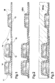
- the contact hole C is formed (see figure 4) inside the oxide layer, it is filled with W through CVD deposition of the tungsten from WF6 to form the W 'plug'; generally between the contact oxide and the W a barrier layer of TiN (or Ti/TiN) is interposed from CVD (Chemical Vapour Deposition) or PVD (Physical Vapour Deposition) to avoid contaminations of WF6 and diffusion of the W through the oxide.
- a transparent UV (Ultra Violet) nitride layer NIT is deposed through a HDP process, with a thickness among 200 ⁇ and 500 ⁇ , as from figure 5.
- the deposed layer NIT is preferably insulating in order to avoid any possible short circuit.
- the deposed layer must be of a material that allows of getting a high selectivity with the BPSG during the contact attack, so that, once the resist is worn out (or it has been consumed) it develops the same function of superior barrier layer (that is above the BPSG layer) in comparison to the attack chemistry.
- the deposed layer is for instance a transparent UV nitride that has high selectivity with the BPSG and does not prevent the reliability performances of the memory cell, particularly if the cell is of flash type.
- Such a layer avoids the formation of contacts called "with double edge", that are critical when the contact dimension is of the order of the 0.2. ⁇ m or smaller than that and the distance between the contacts is of the order of 0.5 ⁇ m.
- the contact attack chemistry will be modified in order to correctly attach the additional protective layer in the first phases (being in the case in object a nitride layer, a dry attack of the protective layer having a chemistry of the type C4F8/O2 will be advantageously used, that allows to have an elevated selectivity with the BPSG underlying oxide), and therefore proceeding in a standard way for instance with the chemistry CHF3/O2, of attack oxide once arrived on the BPSG.
Landscapes
- Internal Circuitry In Semiconductor Integrated Circuit Devices (AREA)
Abstract
Borophosphosilicate glass (BPSG) layer is provided on the surface of an integrated circuit (IC). A transparent ultraviolet (UV) nitride layer is deposited on the BPSG layer by high density plasma (HDP) process. The thickness of nitride layer is between 200-500 Å.
Description
The present invention refers to the construction of integrated circuits.
More particularly it refers to a process for the contact opening definition for
the active element electric connections.
The active elements of an integrated circuit are connected one another
through contacts. The number of contacts in an integrated circuit can vary
from hundred thousands to about ten million.
The dimension reduction of the of the integrated circuits leads to the
realization of contacts having dimensions lower and lower, and they require
more and more precise and delicate processes. Also the possible presence of
extraneous substances existing on the process environment can alter and
contaminate the process in progress.
In view of the state of the art described, it is an object of the present
invention to provide a process for the formation of the contacts in an
integrated circuit that does not have the drawbacks of the known art.
According to the present invention, such object is achieved by means of
a process for the contact opening definition for the active element electric
connections comprising the following phases: forming on the surface of an
integrated circuit a layer of BPSG; forming above the precedent layer, a
transparent layer of nitride UV from a HDP process, having a thickness
among 200Å and 500Å.
The features and the advantages of the present invention will be made
more evident by the following detailed description of a particular
embodiment, illustrated as a non-limiting example in the annexed drawings,
wherein:
The process for the construction of an integrated circuit is normally
composed of the following phases.
At this point, according to the known art the contact mask is exposed,
which foresees two overlapped layers of BARC (Bottom Anti Reflecting
Coating) and of resist, for the masks to be used in the exposure of the DUV
(Deep Ultra Violet) type.
Such layers are necessary to allow the correct definition of the contacts
according to the dimensional specifications required by the product; the
presence of the BARC also avoids the contamination of the resist from the
doped layer of BPSG, fact that if happened it would jeopardize the final
result of the lithographic process.
Then the selective removal of the BPSG, USG layers is effected
through a dry attack of the oxide layers, generally using a chemistry of the
CHF3/CF4/O2 type, usually used for the oxide attack at the contact level.
Once the contact hole C is formed (see figure 4) inside the oxide layer, it is
filled with W through CVD deposition of the tungsten from WF6 to form the
W 'plug'; generally between the contact oxide and the W a barrier layer of
TiN (or Ti/TiN) is interposed from CVD (Chemical Vapour Deposition) or
PVD (Physical Vapour Deposition) to avoid contaminations of WF6 and
diffusion of the W through the oxide. Through dry attack (selective with the
Ti/TiN layer, which is stopped for end-point) is removed (etch back)
therefore the W deposited in excess, giving definitive form to the contact.
The operations of deposition of the AlCu metal layers and the definition of
the circuit interconnections follow.
According to the present invention, after the phase 12, instead of
immediately exposing the contact mask a transparent UV (Ultra Violet)
nitride layer NIT is deposed through a HDP process, with a thickness among
200Å and 500Å, as from figure 5. The deposed layer NIT is preferably
insulating in order to avoid any possible short circuit.
After that, two overlapped layers of BARC and of resist are formed,
when necessary.
The deposed layer must be of a material that allows of getting a high
selectivity with the BPSG during the contact attack, so that, once the resist is
worn out (or it has been consumed) it develops the same function of superior
barrier layer (that is above the BPSG layer) in comparison to the attack
chemistry. To this purpose it could be advantageous that the deposed layer is
for instance a transparent UV nitride that has high selectivity with the BPSG
and does not prevent the reliability performances of the memory cell,
particularly if the cell is of flash type.
The function of such a layer is that of avoiding the direct contact of the
BARC+resist with the BPSG, also in case of prolonged rest of the wafers
with BARC+resist already deposed and before their working (contact
attack). In such a way the defectiveness formation called "corrosion" of the
BPSG layer is avoided, which makes impossible the contact definition and
therefore provokes a yield loss during the device testing.
Besides, such a layer avoids the formation of contacts called "with
double edge", that are critical when the contact dimension is of the order of
the 0.2. µm or smaller than that and the distance between the contacts is of
the order of 0.5µm.
Once the barrier layer has been deposed according to the present
invention, the normal operations of mask exposure of the contact and its
attack is effectuated, as in figure 6. Obviously the contact attack chemistry
will be modified in order to correctly attach the additional protective layer in
the first phases (being in the case in object a nitride layer, a dry attack of the
protective layer having a chemistry of the type C4F8/O2 will be
advantageously used, that allows to have an elevated selectivity with the
BPSG underlying oxide), and therefore proceeding in a standard way for
instance with the chemistry CHF3/O2, of attack oxide once arrived on the
BPSG.
Claims (4)
- Process for the contact opening definition for the active element electric connections comprising the following phases: forming on the surface of an integrated circuit a layer of BPSG; forming above the precedent layer, a transparent layer of nitride UV from a HDP process, having a thickness among 200Å and 500Å.
- Process according to claim 1 characterized in that after the phase of forming a layer of nitride UV there is the phase of forming two overlapped layers of BARC and of resist.
- Process according to claim 1 characterized in that before the phase of forming on the surface of a integrated circuit a BPSG layer, there is the phase of forming a USG oxide layer having a thickness between 500Å and 2500Å.
- Process according to claim 1 characterized in that after the phase of forming two overlapped layers of BARC and of resist there is the phase of chemical attack for the formation of the contact window.
Priority Applications (2)
| Application Number | Priority Date | Filing Date | Title |
|---|---|---|---|
| EP02425558A EP1398830A1 (en) | 2002-09-12 | 2002-09-12 | Process for the contact opening definition for the active element electric connections |
| US10/661,104 US7220686B2 (en) | 2002-09-12 | 2003-09-12 | Process for contact opening definition for active element electrical connections |
Applications Claiming Priority (1)
| Application Number | Priority Date | Filing Date | Title |
|---|---|---|---|
| EP02425558A EP1398830A1 (en) | 2002-09-12 | 2002-09-12 | Process for the contact opening definition for the active element electric connections |
Publications (1)
| Publication Number | Publication Date |
|---|---|
| EP1398830A1 true EP1398830A1 (en) | 2004-03-17 |
Family
ID=31725549
Family Applications (1)
| Application Number | Title | Priority Date | Filing Date |
|---|---|---|---|
| EP02425558A Withdrawn EP1398830A1 (en) | 2002-09-12 | 2002-09-12 | Process for the contact opening definition for the active element electric connections |
Country Status (2)
| Country | Link |
|---|---|
| US (1) | US7220686B2 (en) |
| EP (1) | EP1398830A1 (en) |
Families Citing this family (1)
| Publication number | Priority date | Publication date | Assignee | Title |
|---|---|---|---|---|
| US9123690B1 (en) | 2012-10-18 | 2015-09-01 | University Of South Florida | Systems and methods for forming contact definitions |
Citations (3)
| Publication number | Priority date | Publication date | Assignee | Title |
|---|---|---|---|---|
| US4618541A (en) * | 1984-12-21 | 1986-10-21 | Advanced Micro Devices, Inc. | Method of forming a silicon nitride film transparent to ultraviolet radiation and resulting article |
| US5877095A (en) * | 1994-09-30 | 1999-03-02 | Nippondenso Co., Ltd. | Method of fabricating a semiconductor device having a silicon nitride film made of silane, ammonia and nitrogen |
| US20020111014A1 (en) * | 2001-02-13 | 2002-08-15 | Jeng Pei Reng | Planarization method of inter-layer dielectrics and inter-metal dielectrics |
Family Cites Families (6)
| Publication number | Priority date | Publication date | Assignee | Title |
|---|---|---|---|---|
| US5728453A (en) * | 1995-12-28 | 1998-03-17 | Advanced Micro Devices, Inc. | Method of fabricating topside structure of a semiconductor device |
| US6166439A (en) * | 1997-12-30 | 2000-12-26 | Advanced Micro Devices, Inc. | Low dielectric constant material and method of application to isolate conductive lines |
| US6369453B1 (en) * | 2000-08-11 | 2002-04-09 | Advanced Micro Devices, Inc. | Semiconductor wafer for measurement and recordation of impurities in semiconductor insulators |
| KR100381964B1 (en) * | 2000-11-30 | 2003-04-26 | 삼성전자주식회사 | Method of formimg insulation layer and semiconductor device formed by using the same |
| US7060193B2 (en) * | 2002-07-05 | 2006-06-13 | Chartered Semiconductor Manufacturing Ltd. | Method to form both high and low-k materials over the same dielectric region, and their application in mixed mode circuits |
| US20040048468A1 (en) * | 2002-09-10 | 2004-03-11 | Chartered Semiconductor Manufacturing Ltd. | Barrier metal cap structure on copper lines and vias |
-
2002
- 2002-09-12 EP EP02425558A patent/EP1398830A1/en not_active Withdrawn
-
2003
- 2003-09-12 US US10/661,104 patent/US7220686B2/en not_active Expired - Lifetime
Patent Citations (3)
| Publication number | Priority date | Publication date | Assignee | Title |
|---|---|---|---|---|
| US4618541A (en) * | 1984-12-21 | 1986-10-21 | Advanced Micro Devices, Inc. | Method of forming a silicon nitride film transparent to ultraviolet radiation and resulting article |
| US5877095A (en) * | 1994-09-30 | 1999-03-02 | Nippondenso Co., Ltd. | Method of fabricating a semiconductor device having a silicon nitride film made of silane, ammonia and nitrogen |
| US20020111014A1 (en) * | 2001-02-13 | 2002-08-15 | Jeng Pei Reng | Planarization method of inter-layer dielectrics and inter-metal dielectrics |
Also Published As
| Publication number | Publication date |
|---|---|
| US7220686B2 (en) | 2007-05-22 |
| US20040121589A1 (en) | 2004-06-24 |
Similar Documents
| Publication | Publication Date | Title |
|---|---|---|
| US12489065B2 (en) | Fabrication method of semiconductor structure | |
| US5773314A (en) | Plug protection process for use in the manufacture of embedded dynamic random access memory (DRAM) cells | |
| US7986012B2 (en) | Semiconductor device and process for manufacturing same | |
| US7094672B2 (en) | Method for forming self-aligned contact in semiconductor device | |
| US6884712B2 (en) | Method of manufacturing semiconductor local interconnect and contact | |
| US7888804B2 (en) | Method for forming self-aligned contacts and local interconnects simultaneously | |
| US7935625B2 (en) | Method of forming a metal line of a semiconductor memory device | |
| US7622347B2 (en) | Self-aligned metal electrode to eliminate native oxide effect for metal insulator semiconductor (MIS) capacitor | |
| US6489201B2 (en) | Method for manufacturing a semiconductor device | |
| US7829437B2 (en) | Method of manufacturing a semiconductor device | |
| US6878639B1 (en) | Borderless interconnection process | |
| US8247290B2 (en) | Semiconductor device and method of manufacturing thereof | |
| KR19990025247A (en) | Method of forming electrode protective film of semiconductor device | |
| KR20100008942A (en) | Semiconductor device and manufacturing method thereof | |
| JP5178025B2 (en) | Manufacturing method of semiconductor memory device | |
| US20010014530A1 (en) | Method for manufacturing a semiconductor device | |
| US9006809B2 (en) | Multi-landing contact etching | |
| US7220686B2 (en) | Process for contact opening definition for active element electrical connections | |
| KR100507872B1 (en) | Method for fabrication of semiconductor device | |
| JP3515428B2 (en) | Method for manufacturing semiconductor device | |
| US6426256B1 (en) | Method for fabricating an embedded DRAM with self-aligned borderless contacts | |
| KR100443148B1 (en) | Method For Manufacturing Semiconductor Devices | |
| KR100578230B1 (en) | Bit line formation method using dual damascene process | |
| KR101175275B1 (en) | Method for forming landing plug contact in semiconductor device | |
| KR100528123B1 (en) | Method For Manufacturing Semiconductor Devices |
Legal Events
| Date | Code | Title | Description |
|---|---|---|---|
| PUAI | Public reference made under article 153(3) epc to a published international application that has entered the european phase |
Free format text: ORIGINAL CODE: 0009012 |
|
| AK | Designated contracting states |
Kind code of ref document: A1 Designated state(s): AT BE BG CH CY CZ DE DK EE ES FI FR GB GR IE IT LI LU MC NL PT SE SK TR |
|
| AX | Request for extension of the european patent |
Extension state: AL LT LV MK RO SI |
|
| AKX | Designation fees paid | ||
| REG | Reference to a national code |
Ref country code: DE Ref legal event code: 8566 |
|
| STAA | Information on the status of an ep patent application or granted ep patent |
Free format text: STATUS: THE APPLICATION IS DEEMED TO BE WITHDRAWN |
|
| 18D | Application deemed to be withdrawn |
Effective date: 20040920 |