EP1396893A2 - Method for forming Josephson junction, Josephson junction and apparatus using Josephson junction - Google Patents
Method for forming Josephson junction, Josephson junction and apparatus using Josephson junction Download PDFInfo
- Publication number
- EP1396893A2 EP1396893A2 EP03255199A EP03255199A EP1396893A2 EP 1396893 A2 EP1396893 A2 EP 1396893A2 EP 03255199 A EP03255199 A EP 03255199A EP 03255199 A EP03255199 A EP 03255199A EP 1396893 A2 EP1396893 A2 EP 1396893A2
- Authority
- EP
- European Patent Office
- Prior art keywords
- film
- layer
- substrate
- nbcn
- nbn
- Prior art date
- Legal status (The legal status is an assumption and is not a legal conclusion. Google has not performed a legal analysis and makes no representation as to the accuracy of the status listed.)
- Withdrawn
Links
- 238000000034 method Methods 0.000 title claims description 15
- 239000000758 substrate Substances 0.000 claims abstract description 60
- 238000003491 array Methods 0.000 claims description 13
- 238000010030 laminating Methods 0.000 claims description 9
- 239000000395 magnesium oxide Substances 0.000 description 49
- CPLXHLVBOLITMK-UHFFFAOYSA-N magnesium oxide Inorganic materials [Mg]=O CPLXHLVBOLITMK-UHFFFAOYSA-N 0.000 description 49
- AXZKOIWUVFPNLO-UHFFFAOYSA-N magnesium;oxygen(2-) Chemical compound [O-2].[Mg+2] AXZKOIWUVFPNLO-UHFFFAOYSA-N 0.000 description 49
- 239000010955 niobium Substances 0.000 description 14
- 239000013078 crystal Substances 0.000 description 12
- 239000000463 material Substances 0.000 description 7
- 238000004544 sputter deposition Methods 0.000 description 6
- 229910017107 AlOx Inorganic materials 0.000 description 5
- 239000001307 helium Substances 0.000 description 5
- 229910052734 helium Inorganic materials 0.000 description 5
- SWQJXJOGLNCZEY-UHFFFAOYSA-N helium atom Chemical compound [He] SWQJXJOGLNCZEY-UHFFFAOYSA-N 0.000 description 5
- 239000007788 liquid Substances 0.000 description 5
- VYPSYNLAJGMNEJ-UHFFFAOYSA-N Silicium dioxide Chemical compound O=[Si]=O VYPSYNLAJGMNEJ-UHFFFAOYSA-N 0.000 description 4
- 230000004888 barrier function Effects 0.000 description 4
- 238000006243 chemical reaction Methods 0.000 description 4
- 238000001020 plasma etching Methods 0.000 description 4
- 238000005546 reactive sputtering Methods 0.000 description 4
- 229910021521 yttrium barium copper oxide Inorganic materials 0.000 description 4
- 230000008859 change Effects 0.000 description 3
- 229910052758 niobium Inorganic materials 0.000 description 3
- GUCVJGMIXFAOAE-UHFFFAOYSA-N niobium atom Chemical compound [Nb] GUCVJGMIXFAOAE-UHFFFAOYSA-N 0.000 description 3
- 239000002887 superconductor Substances 0.000 description 3
- 229910010421 TiNx Inorganic materials 0.000 description 2
- XKRFYHLGVUSROY-UHFFFAOYSA-N argon Substances [Ar] XKRFYHLGVUSROY-UHFFFAOYSA-N 0.000 description 2
- 229910052786 argon Inorganic materials 0.000 description 2
- 229910052681 coesite Inorganic materials 0.000 description 2
- 229910052906 cristobalite Inorganic materials 0.000 description 2
- 238000009413 insulation Methods 0.000 description 2
- 238000012986 modification Methods 0.000 description 2
- 230000004048 modification Effects 0.000 description 2
- 238000005121 nitriding Methods 0.000 description 2
- 230000035515 penetration Effects 0.000 description 2
- 230000008569 process Effects 0.000 description 2
- 239000000377 silicon dioxide Substances 0.000 description 2
- 229910052682 stishovite Inorganic materials 0.000 description 2
- 229910052905 tridymite Inorganic materials 0.000 description 2
- XLYOFNOQVPJJNP-UHFFFAOYSA-N water Substances O XLYOFNOQVPJJNP-UHFFFAOYSA-N 0.000 description 2
- 229910017083 AlN Inorganic materials 0.000 description 1
- 229910019794 NbN Inorganic materials 0.000 description 1
- RTAQQCXQSZGOHL-UHFFFAOYSA-N Titanium Chemical compound [Ti] RTAQQCXQSZGOHL-UHFFFAOYSA-N 0.000 description 1
- BLOIXGFLXPCOGW-UHFFFAOYSA-N [Ti].[Sn] Chemical compound [Ti].[Sn] BLOIXGFLXPCOGW-UHFFFAOYSA-N 0.000 description 1
- XAGFODPZIPBFFR-UHFFFAOYSA-N aluminium Chemical compound [Al] XAGFODPZIPBFFR-UHFFFAOYSA-N 0.000 description 1
- 229910052782 aluminium Inorganic materials 0.000 description 1
- 238000005256 carbonitriding Methods 0.000 description 1
- 238000001816 cooling Methods 0.000 description 1
- 230000007547 defect Effects 0.000 description 1
- 230000000694 effects Effects 0.000 description 1
- 239000007772 electrode material Substances 0.000 description 1
- 238000005516 engineering process Methods 0.000 description 1
- 238000004299 exfoliation Methods 0.000 description 1
- 238000002955 isolation Methods 0.000 description 1
- 238000004519 manufacturing process Methods 0.000 description 1
- 150000002822 niobium compounds Chemical class 0.000 description 1
- 238000007254 oxidation reaction Methods 0.000 description 1
- 239000004065 semiconductor Substances 0.000 description 1
- 238000001179 sorption measurement Methods 0.000 description 1
- 239000010936 titanium Substances 0.000 description 1
- 229910052719 titanium Inorganic materials 0.000 description 1
- 230000010356 wave oscillation Effects 0.000 description 1
Images





Classifications
-
- H—ELECTRICITY
- H03—ELECTRONIC CIRCUITRY
- H03M—CODING; DECODING; CODE CONVERSION IN GENERAL
- H03M1/00—Analogue/digital conversion; Digital/analogue conversion
- H03M1/66—Digital/analogue converters
- H03M1/74—Simultaneous conversion
- H03M1/80—Simultaneous conversion using weighted impedances
-
- G—PHYSICS
- G01—MEASURING; TESTING
- G01R—MEASURING ELECTRIC VARIABLES; MEASURING MAGNETIC VARIABLES
- G01R33/00—Arrangements or instruments for measuring magnetic variables
- G01R33/02—Measuring direction or magnitude of magnetic fields or magnetic flux
- G01R33/035—Measuring direction or magnitude of magnetic fields or magnetic flux using superconductive devices
- G01R33/0354—SQUIDS
-
- H—ELECTRICITY
- H03—ELECTRONIC CIRCUITRY
- H03B—GENERATION OF OSCILLATIONS, DIRECTLY OR BY FREQUENCY-CHANGING, BY CIRCUITS EMPLOYING ACTIVE ELEMENTS WHICH OPERATE IN A NON-SWITCHING MANNER; GENERATION OF NOISE BY SUCH CIRCUITS
- H03B15/00—Generation of oscillations using galvano-magnetic devices, e.g. Hall-effect devices, or using superconductivity effects
-
- H—ELECTRICITY
- H03—ELECTRONIC CIRCUITRY
- H03K—PULSE TECHNIQUE
- H03K19/00—Logic circuits, i.e. having at least two inputs acting on one output; Inverting circuits
- H03K19/02—Logic circuits, i.e. having at least two inputs acting on one output; Inverting circuits using specified components
- H03K19/195—Logic circuits, i.e. having at least two inputs acting on one output; Inverting circuits using specified components using superconductive devices
- H03K19/1954—Logic circuits, i.e. having at least two inputs acting on one output; Inverting circuits using specified components using superconductive devices with injection of the control current
-
- H—ELECTRICITY
- H10—SEMICONDUCTOR DEVICES; ELECTRIC SOLID-STATE DEVICES NOT OTHERWISE PROVIDED FOR
- H10N—ELECTRIC SOLID-STATE DEVICES NOT OTHERWISE PROVIDED FOR
- H10N60/00—Superconducting devices
- H10N60/01—Manufacture or treatment
- H10N60/0912—Manufacture or treatment of Josephson-effect devices
-
- H—ELECTRICITY
- H10—SEMICONDUCTOR DEVICES; ELECTRIC SOLID-STATE DEVICES NOT OTHERWISE PROVIDED FOR
- H10N—ELECTRIC SOLID-STATE DEVICES NOT OTHERWISE PROVIDED FOR
- H10N60/00—Superconducting devices
- H10N60/10—Junction-based devices
- H10N60/12—Josephson-effect devices
Definitions
- the present invention relates to a method for forming Josephson junction (device) and a Josephson junction formed by the method and apparatus using the Josephson Junction formed by the method.
- a Josephson junction is an element comprising two superconductors slightly joined, and the junction is used in isolation or joined with a superconductive inductance line so as to serve a function such as frequency-voltage conversion, magnetic flux-voltage conversion, and ultra high-speed/low-power consumption logic switching.
- the frequency-voltage conversion function is explained as an example below.
- n is an integer
- the voltage "V" in the formula (1) changes only depending on change of the frequency f of the electromagnetic wave to be irradiated, and does not change depending on change of material of the element, dimensions, temperature, etc.
- Nb/AlOx/Nb junction is used, which is formed by using a heat oxidization film (AlOx) of aluminum as a barrier, and using a niobium (Nb) film as an electrode.
- AlOx heat oxidization film
- Nb niobium
- Nb/AlOx/Nb junction An operation of the Nb/AlOx/Nb junction is mostly performed in liquid helium (4.2K). This is because the superconductivity critical temperature (Tc) of Nb is relatively low, that is, about 9 K.
- Liquid helium can be purchased comparatively easily from a private contractor in advanced countries, such as Japan, the U.S., and Europe. However, the price is 1000 yen to several thousand yen per liter. For this reason, when it is necessary to regularly operate the junction element like a voltage standard element or an element for detecting the millimeter waves or sub-millimeter waves which come from the universe, the cost for cooling down the element is increased.
- Such a Josephson junction is divided roughly into two groups.
- a Josephson junction of the first group uses nitriding niobium (NbN) which has a suitable composition ratio or carbonitriding niobium (NbCN) which has a suitable composition ratio as an electrode material.
- NbN nitriding niobium
- NbCN carbonitriding niobium
- Both niobium compounds have superconductivity critical temperature Tc exceeding 15K, and such Josephson junction which uses them as material of an electrode can be operated in 8-12K. This range of temperature is realizable with a commercially available small and low power freezer.
- a Josephson junction in the second group uses, as material of an electrode, a high temperature oxide superconductor, especially YBCO which has a suitable composition ratio.
- the YBCO having a suitable composition ratio has the superconductivity critical temperature Tc exceeding 90K, and a Josephson junction made from YBCO can be operated also in the temperature exceeding 50K.
- the formed film turns into a multi-crystal film.
- the magnetic field penetration depth of the multi-crystal NbN film and the NbCN film is usually about 300 nm. Therefore, in order to avoid an increase of a kinetic inductance, it is necessary to set thickness of the NbN film or a NbCN film used for the electrode of a Josephson junction to 300nm or more. The thickness is about 3 times as thick as that of the Nb film used for the electrode of a Josephson junction. Increase of the thickness of the Josephson junction electrode brings about increase of the thickness of an insulated layer or a wiring layer, and finally causes exfoliation of the film by increase of the stress in a film.
- single crystal magnesium oxide which has the lattice suitable for use with NbN or NbCN has been tried to use as a substrate. It is known that, under suitable sputtering conditions, epitaxial growth of NbN or NbCN deposited on the single crystal MgO is carried out, and they become a high quality film with few defects. As the result, the magnetic field penetration depth in a film is set to about 100 nm. That is, the above-mentioned problem can be solved by using the NbN film or NbCN film which is formed on the single crystal MgO substrate, for the electrode of a Josephson junction,.
- single crystal MgO is very expensive.
- single crystal MgO with a 3 inch diameter and a 0.5 mm thickness costs 100,000 yen or more per sheet.
- NbN or NbCN as material of an electrode
- a method for forming a Josephson junction comprising the following steps of forming a two-layer film having an amorphous MgO layer and a high orientation MgO layer on a Si substrate, and laminating a NbN film or a NbCN film on the two-layer.
- a Josephson junction may be produced by the method for forming a Josephson junction.
- a two-layer film which consists of amorphous MgO layer and crystal MgO layer having strong orientation is formed on a Si wafer by sputtering, and a NbN film or a NbCN film is deposited on the two layer by reactive sputtering, the product of which is used for an electrode, whereby a Josephson junction is created.
- Josephson junction array has at least one Josephson junction comprising a Si substrate, a two layer film comprising an amorphous MgO layer and a high orientation MgO layer on the Si substrate, and a NbN film or a NbCN film laminated on the two layer film.
- a digital to analog converter has Josephson junction arrays comprising Josephson junctions, wherein at least one of the Josephson junctions comprises a Si substrate, a two layer film comprising an amorphous MgO layer and a high orientation MgO layer on the Si substrate, and a NbN film or a NbCN film laminated on the two layer film.
- Josephson voltage generating apparatus has a digital to analog converter comprising junction arrays for programmable converter using Josephson junctions, wherein at least one of the Josephson junctions comprises a Si substrate, a two layer film comprising an amorphous MgO layer and a high orientation MgO layer on the Si substrate, and a NbN film or a NbCN film laminated on the two layer film.
- a Josephson voltage standard apparatus has a digital to analog converter comprising junction arrays for programmable converter using at least one Josephson junction, wherein at least one of the Josephson junctions comprises a Si substrate, a two layer film comprising an amorphous MgO layer and a high orientation MgO layer on the Si substrate, and a NbN film or a NbCN film laminated on the two layer film.
- a superconducting sub-millimeter wave oscillator has at least one Josephson junction comprising a Si substrate, a two layer film comprising an amorphous MgO layer and a high orientation MgO layer on the Si substrate, and a NbN film or a NbCN film laminated on the two layer film.
- a superconducting quantum interference device has at least one Josephson junction comprising a Si substrate, a two layer film comprising an amorphous MgO layer and a high orientation MgO layer on the Si substrate, and a NbN film or a NbCN film laminated on the two layer film.
- a superconductivity digital integrated circuit has at least one Josephson junction comprising a Si substrate, a two layer film comprising an amorphous MgO layer and a high orientation MgO layer on the Si substrate, and a NbN film or a NbCN film laminated on the two layer film.
- the NbN film or the NbCN film is used as an electrode.
- a Si wafer 1 (a substrate) is washed with pure water.
- the surface of the substrate is cleaned and surface adsorption water thereon is removed by argon ion.
- a MgO double layer 4 comprising amorphous MgO film 2 with a 5 nm thickness and a high orientation MgO film 3 with a 5 nm thickness is formed by a sputter deposition.
- a NbN film 5 with a 100 nm film thickness is formed on the MgO two-layer 4 by reactive sputtering.
- a resist pattern 6 for a lower wiring electrode 7 is formed as shown in Fig. 1D.
- the NbN film 5 is processed and the lower wiring electrode 7 is shaped depending on the shape of the resist pattern as shown in Fig. 1E.
- a three-layer film 11 which consists of a NbN film 8 with a 10 nm thickness, a nitriding titanium (TiN) film 9 with a 35 nm thickness, and a NbN film 10 with a 10 nm thickness is created all over the wafer.
- a resist pattern 12 for a junction portion is formed in Fig. 1G.
- the three-layer film 11 is processed by reactive ion etching so as to form a junction portion 13.
- the wafer is moved to another sputtering apparatus and a SiO 2 insulation film 14 with a thickness of 100nm is deposited all over the wafer as shown in Fig. 1I.
- the SiO 2 insulation film 14 is processed so as to create a contact hole 15 as shown in Fig. 1J.
- a NbN film 16 with a thickness of 300 nm is created all over a wafer by reactive sputtering as shown in Fig. 1K.
- the NbN film 16 is processed by reactive ion etching, and the upper wiring electrode 17 is determined.
- the Josephson junction according to the present invention may be used for a two-layer laminating type Josephson junction which has been proposed as shown in Fig 2. Further, the Josephson junction may be used for a three-layer laminating type Josephson junction as shown in Fig. 3. Also see Yamamori et al., "NbN/TiNx/NbN/TiNx/NbN double-barrier junction arrays for programmable voltage standards, Applied Physics Letters, Vol.80, No.8, pp.1415-1417, and those (2002).
- barrier material such as TiN, NbN, AlN, and MgO, it is possible to make the thickness of the superconductivity middle layer 18 and the barrier layer 19 smaller than that of the conventional multi-layer laminating type Josephson junction.
- An epitaxial NbN film and an epitaxial NbCN film have low surface resistance by more than 1 digit lower than that of a polycrystalline film in the frequency band of 0.5-1.0THz. See Kohjiro et al., Surface resistance of epitaxial and polycrystalline NbCN films in sub-milimmeter wave region, IEEE Transactions on Applied Superconductivity, Vol.3, No.2, pp.1765-1767, 1993.
- the sub-millimeter wave oscillation element which uses a NbN film or a NbCN film as an electrode is created on the expensive single crystal MgO substrate.
- Fig. 4 shows a junction array for a programmable Josephson voltage standard, in which a plurality of josephson junctions are connected in series.
- the Josephson junctions are shown as "X". All or at least one of the Josephson Junctions comprise a Si substrate, a two layer film comprising an amorphous MgO layer and a high orientation MgO layer on the Si substrate, and a NbN film or a NbCN film laminated on the two layer film.
- the Josephson junctions according to the present invention can be used for a digital to analog converter.
- Fig. 5 shows the digital to analog converter for a programmable voltage standard.
- all or at least one of the Josephson junction comprises a Si substrate, a two layer film comprising an amorphous MgO layer and a high orientation MgO layer on the Si substrate, and a NbN film or a NbCN film laminated on the two layer film.
- the digital to analog converter has a terminal to which microwave is input and a terminal resistor.
- the NbN film or the NbCN film is used as an electrode.
- the output voltage V out is determined by arbitrarily selecting groups of Josephson junctions, whose number is power of 2.
- Fig. 6 shows a Josephson voltage generating apparatus (system) using Josephson junction arrays to which the Josephson junctions according to the present invention are applied.
- the Josephson junction arrays are provided on a chip of the Josephson voltage generating apparatus (system). All or at least one of the Josephson Junctions comprise a Si substrate, a two layer film comprising an amorphous MgO layer and a high orientation MgO layer on the Si substrate, and a NbN film or a NbCN film laminated on the two layer film.
- the NbN film or the NbCN film is used as an electrode.
- the Josephson voltage may be applied to a Josephson voltage standard apparatus (system).
- Fig. 7 shows a schematic view of the Josephson voltage standard apparatus (system).
- a digital to analog converter having Josephson junction arrays comprising Josephson junctions according to the present invention is provided on a chip of the Josephson voltage standard apparatus.
- All or at least one of the Josephson Junctions comprise a Si substrate, a two layer film comprising an amorphous MgO layer and a high orientation MgO layer on the Si substrate, and a NbN film or a NbCN film laminated on the two layer film.
- the NbN film or the NbCN film is used as an electrode.
- the NbN film or the NbCN film is used as an electrode.
- a digital to analog converter having Josephson junction arrays for a programmable voltage standard is shown.
- the digital to analog converter is provided on a chip of the Josephson voltage generating apparatus (system) shown in Fig. 7.
- the Josephson junctions according to the present invention are provided in each of arrays.
- the Josephson junction arrays having the Josephson junctions according to the present invention are provided in the digital to analog converter, and the digital to analog converter is provided on the chip of the Josephson voltage standard apparatus.
- All or at least one of the Josephson Junctions comprise a Si substrate, a two layer film comprising an amorphous MgO layer and a high orientation MgO layer on the Si substrate, and a NbN film or a NbCN film laminated on the two layer film.
- the NbN film or the NbCN film is used as an electrode.
- Fig. 9 shows a superconducting sub-millimeter wave oscillator to which the Josephson junction according to the present invention is applied.
- the Josephson Junction comprises a Si substrate, a two layer film comprising an amorphous MgO layer and a high orientation MgO layer on the Si substrate, and a NbN film or a NbCN film laminated on the two layer film.
- the NbN film or the NbCN film is used as an electrode.
- Fig. 10 shows a superconducting quantum interference device to which the Josephson Junctions according to the present invention are applied.
- All or at least one of the Josephson Junctions comprise a Si substrate, a two layer film comprising an amorphous MgO layer and a high orientation MgO layer on the Si substrate, and a NbN film or a NbCN film laminated on the two layer film.
- the NbN film or the NbCN film is used as an electrode.
- Josephson junctions may be applied to a superconducting digital integrated circuit (Comparator).
- Fig. 11 Josephson junctions J 1 to J 5 according to the present invention are shown. All or at least one of the Josephson Junctions comprise a Si substrate, a two layer film comprising an amorphous MgO layer and a high orientation MgO layer on the Si substrate, and a NbN film or a NbCN film laminated on the two layer film.
- the NbN film or the NbCN film is used as an electrode.
- the Josephson junction according to the present invention may be applied to any devices, apparatuses, systems, circuits and the like.
Landscapes
- Physics & Mathematics (AREA)
- Engineering & Computer Science (AREA)
- Condensed Matter Physics & Semiconductors (AREA)
- General Physics & Mathematics (AREA)
- Computer Hardware Design (AREA)
- Computing Systems (AREA)
- General Engineering & Computer Science (AREA)
- Mathematical Physics (AREA)
- Theoretical Computer Science (AREA)
- Manufacturing & Machinery (AREA)
- Superconductor Devices And Manufacturing Methods Thereof (AREA)
Abstract
Description
- The present invention relates to a method for forming Josephson junction (device) and a Josephson junction formed by the method and apparatus using the Josephson Junction formed by the method.
- A Josephson junction (device) is an element comprising two superconductors slightly joined, and the junction is used in isolation or joined with a superconductive inductance line so as to serve a function such as frequency-voltage conversion, magnetic flux-voltage conversion, and ultra high-speed/low-power consumption logic switching.
- The frequency-voltage conversion function is explained as an example below.
- When electromagnetic wave of frequency f is irradiated at a Josephson junction, voltage V shown by the following formula (1) is generated between two terminals of the Josephson junction.
- In the formula shown above, "n" is an integer, and "KJ-90" is Josephson constant (=2e/h=483,597.9 GHz/V).
- The voltage "V" in the formula (1) changes only depending on change of the frequency f of the electromagnetic wave to be irradiated, and does not change depending on change of material of the element, dimensions, temperature, etc.
- Since the frequency of the electromagnetic wave can be determined with very high accuracy (1/1011 of accuracy), voltage that the Josephson junction generates can be also determined with a very high accuracy (1/109 of accuracy). Such a frequency-voltage conversion function is theoretically unrealizable in elements other than such a Josephson junction. Therefore, in the major standard research organizations in the world, the element using a Josephson junction device is used for the primary standard of voltage.
- In almost all Josephson junction devices used for practical application now, Nb/AlOx/Nb junction is used, which is formed by using a heat oxidization film (AlOx) of aluminum as a barrier, and using a niobium (Nb) film as an electrode.
- This is because, in case of a Nb/AlOx/Nb junction, (1) an uniform electrical property can be obtained when a large number of junctions are accumulated on a substrate with high density; (2) it is easy to control electrical properties such as criticality current density and usual state resistance; and (3) it is hard for such properties to deteriorate by the heat cycle between the room temperature and cryogenic temperature.
- An operation of the Nb/AlOx/Nb junction is mostly performed in liquid helium (4.2K). This is because the superconductivity critical temperature (Tc) of Nb is relatively low, that is, about 9 K.
- Liquid helium can be purchased comparatively easily from a private contractor in advanced nations, such as Japan, the U.S., and Europe. However, the price is 1000 yen to several thousand yen per liter. For this reason, when it is necessary to regularly operate the junction element like a voltage standard element or an element for detecting the millimeter waves or sub-millimeter waves which come from the universe, the cost for cooling down the element is increased.
- Moreover, in the country and area where liquid helium cannot be obtained easily, it is difficult to operate such an element itself.
- It is possible to cool down and to operate a Josephson junction as a means to solve this problem, using a freezer, without liquid helium. However, such a freezer which can cool down the junction to the liquid helium temperature is very expensive and needs large electric power. For this reason, putting, into practical use, the Josephson junction which can be cooled down and operated with the small freezer of low electric power is desired.
- Such a Josephson junction is divided roughly into two groups. A Josephson junction of the first group uses nitriding niobium (NbN) which has a suitable composition ratio or carbonitriding niobium (NbCN) which has a suitable composition ratio as an electrode material. Both niobium compounds have superconductivity critical temperature Tc exceeding 15K, and such Josephson junction which uses them as material of an electrode can be operated in 8-12K. This range of temperature is realizable with a commercially available small and low power freezer.
- A Josephson junction in the second group uses, as material of an electrode, a high temperature oxide superconductor, especially YBCO which has a suitable composition ratio. The YBCO having a suitable composition ratio has the superconductivity critical temperature Tc exceeding 90K, and a Josephson junction made from YBCO can be operated also in the temperature exceeding 50K.
- However, technology of accumulating on a substrate the Josephson junctions using high temperature oxide superconductors, such as YBCO, as material of an electrode, and acquiring the uniform characteristic has not been realized yet. For this reason, there is no Josephson junction which can be replaced with present Nb/AlOx/Nb junction other than Josephson junctions belonging to the first group, that is, those using i.e., NbN, or NbCN as material of an electrode.
- When a NbN film or a NbCN film is deposited by reactive sputtering on a Si wafer, since crystal lattice compatibility between the Si wafer and the NbN film, or the NbCN film is not good, the formed film turns into a multi-crystal film. The magnetic field penetration depth of the multi-crystal NbN film and the NbCN film is usually about 300 nm. Therefore, in order to avoid an increase of a kinetic inductance, it is necessary to set thickness of the NbN film or a NbCN film used for the electrode of a Josephson junction to 300nm or more. The thickness is about 3 times as thick as that of the Nb film used for the electrode of a Josephson junction. Increase of the thickness of the Josephson junction electrode brings about increase of the thickness of an insulated layer or a wiring layer, and finally causes exfoliation of the film by increase of the stress in a film.
- To find solutions to this problem, single crystal magnesium oxide (MgO) which has the lattice suitable for use with NbN or NbCN has been tried to use as a substrate. It is known that, under suitable sputtering conditions, epitaxial growth of NbN or NbCN deposited on the single crystal MgO is carried out, and they become a high quality film with few defects. As the result, the magnetic field penetration depth in a film is set to about 100 nm. That is, the above-mentioned problem can be solved by using the NbN film or NbCN film which is formed on the single crystal MgO substrate, for the electrode of a Josephson junction,.
- However, commercially available single crystal MgO is very expensive. For example, single crystal MgO with a 3 inch diameter and a 0.5 mm thickness costs 100,000 yen or more per sheet. For this reason, in order to create the general-purpose Josephson junction which uses NbN or NbCN as material of an electrode, it is substantially difficult to adopt a single crystal MgO as a substrate.
- It is an object of the present invention to solve the above described problem.
- According to the present invention, a method for forming a Josephson junction, comprising the following steps of forming a two-layer film having an amorphous MgO layer and a high orientation MgO layer on a Si substrate, and laminating a NbN film or a NbCN film on the two-layer.
- Further, according to the present invention, a Josephson junction may be produced by the method for forming a Josephson junction.
- Furthermore, according to the present invention, a two-layer film which consists of amorphous MgO layer and crystal MgO layer having strong orientation is formed on a Si wafer by sputtering, and a NbN film or a NbCN film is deposited on the two layer by reactive sputtering, the product of which is used for an electrode, whereby a Josephson junction is created.
- Further, according to the present invention, Josephson junction array has at least one Josephson junction comprising a Si substrate, a two layer film comprising an amorphous MgO layer and a high orientation MgO layer on the Si substrate, and a NbN film or a NbCN film laminated on the two layer film.
- Furthermore, according to the present invention, a digital to analog converter has Josephson junction arrays comprising Josephson junctions, wherein at least one of the Josephson junctions comprises a Si substrate, a two layer film comprising an amorphous MgO layer and a high orientation MgO layer on the Si substrate, and a NbN film or a NbCN film laminated on the two layer film.
- Still further, according to the present invention, Josephson voltage generating apparatus has a digital to analog converter comprising junction arrays for programmable converter using Josephson junctions, wherein at least one of the Josephson junctions comprises a Si substrate, a two layer film comprising an amorphous MgO layer and a high orientation MgO layer on the Si substrate, and a NbN film or a NbCN film laminated on the two layer film.
- Further, according to the present invention, a Josephson voltage standard apparatus has a digital to analog converter comprising junction arrays for programmable converter using at least one Josephson junction, wherein at least one of the Josephson junctions comprises a Si substrate, a two layer film comprising an amorphous MgO layer and a high orientation MgO layer on the Si substrate, and a NbN film or a NbCN film laminated on the two layer film.
- According to the present invention, a superconducting sub-millimeter wave oscillator has at least one Josephson junction comprising a Si substrate, a two layer film comprising an amorphous MgO layer and a high orientation MgO layer on the Si substrate, and a NbN film or a NbCN film laminated on the two layer film.
- According to the present invention, a superconducting quantum interference device has at least one Josephson junction comprising a Si substrate, a two layer film comprising an amorphous MgO layer and a high orientation MgO layer on the Si substrate, and a NbN film or a NbCN film laminated on the two layer film.
- According to the present invention, a superconductivity digital integrated circuit has at least one Josephson junction comprising a Si substrate, a two layer film comprising an amorphous MgO layer and a high orientation MgO layer on the Si substrate, and a NbN film or a NbCN film laminated on the two layer film.
- According to the present invention, the NbN film or the NbCN film is used as an electrode.
- The present inventions will now be described by way of example with reference to the following figures in which:
- Figs. 1A-1L shows steps of a Josephson junction forming process;
- Fig. 2 is a cross sectional view of a double layer laminating type Josephson junction;
- Fig. 3 is a cross sectional view of triple laminating type Josephson junction;
- Fig. 4 is a schematic view of a junction array for a programmable Josephson voltage standard;
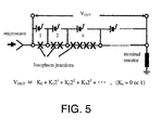
- Fig. 5 is a digital to analog converter for a programmable voltage standard according to the present invention;
- Fig. 6 is a schematic view of a Josephson voltage generating apparatus according to the present invention;
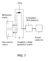
- Fig. 7 is a schematic view of a Josephson voltage standard system;
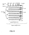
- Fig. 8 is a schematic view of a digital to analog converter provided on a chip of the Josephson voltage standard system shown in Fig. 7;
- Fig. 9 is a schematic view of a superconducting sub-millimeter wave oscillator according to the present invention;
- Fig. 10 is a schematic view of a superconducting quantum interference device; and
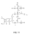
- Fig. 11 is a schematic view of a superconducting digital integrated circuit (Comparator).
-
- Description of a method according to the present invention will be given below referring to Fig. 1.
- As shown in Fig. 1A, a Si wafer 1 (a substrate) is washed with pure water. In a sputtering chamber, the surface of the substrate is cleaned and surface adsorption water thereon is removed by argon ion.
- Next, as shown in Fig. 1B, a MgO double layer 4 comprising amorphous MgO film 2 with a 5 nm thickness and a high orientation MgO film 3 with a 5 nm thickness is formed by a sputter deposition.
- In Fig. 1C, a NbN film 5 with a 100 nm film thickness is formed on the MgO two-layer 4 by reactive sputtering.
- After that, a resist pattern 6 for a lower wiring electrode 7 is formed as shown in Fig. 1D.
- By reactive ion etching, the NbN film 5 is processed and the lower wiring electrode 7 is shaped depending on the shape of the resist pattern as shown in Fig. 1E.
- In Fig. 1F, after the processed wafer is returned to the sputtering apparatus and the surface of the wafer is cleaned by argon ion, a three-layer film 11 which consists of a NbN film 8 with a 10 nm thickness, a nitriding titanium (TiN) film 9 with a 35 nm thickness, and a NbN film 10 with a 10 nm thickness is created all over the wafer.
- And then, a resist pattern 12 for a junction portion is formed in Fig. 1G.
- Further, in Fig. 1H, the three-layer film 11 is processed by reactive ion etching so as to form a junction portion 13.
- Next, the wafer is moved to another sputtering apparatus and a SiO2 insulation film 14 with a thickness of 100nm is deposited all over the wafer as shown in Fig. 1I.
- By reactive ion etching, the SiO2 insulation film 14 is processed so as to create a contact hole 15 as shown in Fig. 1J.
- In order to create an upper wiring electrode 17, a NbN film 16 with a thickness of 300 nm is created all over a wafer by reactive sputtering as shown in Fig. 1K.
- The NbN film 16 is processed by reactive ion etching, and the upper wiring electrode 17 is determined.
- Although the above-mentioned example is a single laminating Josephson junction, the Josephson junction according to the present invention may be used for a two-layer laminating type Josephson junction which has been proposed as shown in Fig 2. Further, the Josephson junction may be used for a three-layer laminating type Josephson junction as shown in Fig. 3. Also see Yamamori et al., "NbN/TiNx/NbN/TiNx/NbN double-barrier junction arrays for programmable voltage standards, Applied Physics Letters, Vol.80, No.8, pp.1415-1417, and those (2002).
- It is desirable to make thickness of a superconductivity middle layer 18 and barrier layers 19 as small as possible in creation of such a multi-layer laminating type Josephson junction from a viewpoint of raising the production yield.
- If suitable barrier material, such as TiN, NbN, AlN, and MgO, are chosen, it is possible to make the thickness of the superconductivity middle layer 18 and the barrier layer 19 smaller than that of the conventional multi-layer laminating type Josephson junction.
- An epitaxial NbN film and an epitaxial NbCN film have low surface resistance by more than 1 digit lower than that of a polycrystalline film in the frequency band of 0.5-1.0THz. See Kohjiro et al., Surface resistance of epitaxial and polycrystalline NbCN films in sub-milimmeter wave region, IEEE Transactions on Applied Superconductivity, Vol.3, No.2, pp.1765-1767, 1993.
- For this reason, the sub-millimeter wave oscillation element which uses a NbN film or a NbCN film as an electrode is created on the expensive single crystal MgO substrate.
- If the method according to the present invention is used, it is possible to create those elements on an inexpensive Si wafer.
- Fig. 4 shows a junction array for a programmable Josephson voltage standard, in which a plurality of josephson junctions are connected in series. The Josephson junctions are shown as "X". All or at least one of the Josephson Junctions comprise a Si substrate, a two layer film comprising an amorphous MgO layer and a high orientation MgO layer on the Si substrate, and a NbN film or a NbCN film laminated on the two layer film.
- Moreover, the Josephson junctions according to the present invention can be used for a digital to analog converter. Fig. 5 shows the digital to analog converter for a programmable voltage standard. In Fig. 5, all or at least one of the Josephson junction comprises a Si substrate, a two layer film comprising an amorphous MgO layer and a high orientation MgO layer on the Si substrate, and a NbN film or a NbCN film laminated on the two layer film. The digital to analog converter has a terminal to which microwave is input and a terminal resistor. In the digital to analog converter, the NbN film or the NbCN film is used as an electrode. The output voltage Vout is determined by arbitrarily selecting groups of Josephson junctions, whose number is power of 2. The output voltage Vout is represented as follows:
- Fig. 6 shows a Josephson voltage generating apparatus (system) using Josephson junction arrays to which the Josephson junctions according to the present invention are applied. The Josephson junction arrays are provided on a chip of the Josephson voltage generating apparatus (system). All or at least one of the Josephson Junctions comprise a Si substrate, a two layer film comprising an amorphous MgO layer and a high orientation MgO layer on the Si substrate, and a NbN film or a NbCN film laminated on the two layer film. The NbN film or the NbCN film is used as an electrode.
- Further, the Josephson voltage may be applied to a Josephson voltage standard apparatus (system). Fig. 7 shows a schematic view of the Josephson voltage standard apparatus (system). A digital to analog converter having Josephson junction arrays comprising Josephson junctions according to the present invention is provided on a chip of the Josephson voltage standard apparatus. All or at least one of the Josephson Junctions comprise a Si substrate, a two layer film comprising an amorphous MgO layer and a high orientation MgO layer on the Si substrate, and a NbN film or a NbCN film laminated on the two layer film. The NbN film or the NbCN film is used as an electrode. In Josephson voltage standard apparatus, the NbN film or the NbCN film is used as an electrode.
- In Fig. 8, a digital to analog converter having Josephson junction arrays for a programmable voltage standard is shown. The digital to analog converter is provided on a chip of the Josephson voltage generating apparatus (system) shown in Fig. 7. The Josephson junctions according to the present invention are provided in each of arrays. Thus, the Josephson junction arrays having the Josephson junctions according to the present invention, are provided in the digital to analog converter, and the digital to analog converter is provided on the chip of the Josephson voltage standard apparatus. All or at least one of the Josephson Junctions comprise a Si substrate, a two layer film comprising an amorphous MgO layer and a high orientation MgO layer on the Si substrate, and a NbN film or a NbCN film laminated on the two layer film. The NbN film or the NbCN film is used as an electrode.
- Fig. 9 shows a superconducting sub-millimeter wave oscillator to which the Josephson junction according to the present invention is applied. The Josephson Junction comprises a Si substrate, a two layer film comprising an amorphous MgO layer and a high orientation MgO layer on the Si substrate, and a NbN film or a NbCN film laminated on the two layer film. In the superconducting sub-millimeter wave oscillator, the NbN film or the NbCN film is used as an electrode.
- Fig. 10 shows a superconducting quantum interference device to which the Josephson Junctions according to the present invention are applied. All or at least one of the Josephson Junctions comprise a Si substrate, a two layer film comprising an amorphous MgO layer and a high orientation MgO layer on the Si substrate, and a NbN film or a NbCN film laminated on the two layer film. In the superconducting quantum interference device, the NbN film or the NbCN film is used as an electrode.
- Further, Josephson junctions may be applied to a superconducting digital integrated circuit (Comparator). In Fig. 11, Josephson junctions J1 to J5 according to the present invention are shown. All or at least one of the Josephson Junctions comprise a Si substrate, a two layer film comprising an amorphous MgO layer and a high orientation MgO layer on the Si substrate, and a NbN film or a NbCN film laminated on the two layer film. In the superconducting quantum interference device, the NbN film or the NbCN film is used as an electrode.
- Thus, the Josephson junction according to the present invention may be applied to any devices, apparatuses, systems, circuits and the like.
- The following effects are acquired by adopting the method according to the present invention:
- (1) It is possible to substantially reduce the cost since an inexpensive Si wafer having a large area is used instead of an expensive single crystal MgO substrate.
- (2) Although an MgO substrate has restriction in a size, thickness, or form, if a Si wafer is used, the general-purpose process apparatus for semiconductors, such as i line stepper, can be used.
-
- Although only some exemplary embodiments of this invention have been described in detail above, those skilled in the art will readily appreciated that many modifications are possible in the exemplary embodiments without materially departing from the novel teachings and advantages of this invention. Accordingly, all such modifications are intended to be included within the scope of this invention.
Claims (19)
- A method for forming a Josephson junction, the method comprising the following steps of:forming a two-layer film having an amorphous MgO layer and a high orientation MgO layer on a Si substrate; andlaminating a NbN film or an NbCN film on the two-layer.
- The method according to claim 1, wherein the NbN film or the NbCN film is used as an electrode.
- A Josephson junction formed by the method according to claim 1.
- A Josephson junction comprising:a Si substrate;a two layer film comprising an amorphous MgO layer and a high orientation MgO layer on the Si substrate; anda NbN film or a NbCN film laminated on the two layer film.
- The Josephson junction according to claim 4, wherein the NbN film or the NbCN film is used as an electrode.
- A Josephson junction array comprising: at least one Josephson junction comprising a Si substrate, a two layer film comprising an amorphous MgO layer and a high orientation MgO layer on the Si substrate, and a NbN film or a NbCN film laminated on the two layer film.
- The Josephson junction array according to claim 6, wherein the NbN film or the NbCN film is used as an electrode.
- A digital to analog converter comprising: Josephson junction arrays comprising Josephson junctions, wherein at least one of the Josephson junctions comprises a Si substrate, a two layer film comprising an amorphous MgO layer and a high orientation MgO layer on the Si substrate, and a NbN film or a NbCN film laminated on the two layer film.
- The Josephson junction array according to claim 8, wherein the NbN film or the NbCN film is used as an electrode.
- A Josephson voltage generating apparatus comprising: a digital to analog converter comprising junction arrays for programmable converter using Josephson junctions, wherein at least one of the Josephson junctions comprises a Si substrate, a two layer film comprising an amorphous MgO layer and a high orientation MgO layer on the Si substrate, and a NbN film or a NbCN film laminated on the two layer film.
- The Josephson junction array according to claim 10, wherein the NbN film or the NbCN film is used as an electrode.
- A Josephson voltage standard apparatus comprising: a digital to analog converter comprising junction arrays for programmable converter using at least one Josephson junction, wherein at least one of the Josephson junctions comprises a Si substrate, a two layer film comprising an amorphous MgO layer and a high orientation MgO layer on the Si substrate, and a NbN film or a NbCN film laminated on the two layer film.
- The Josephson junction array according to claim 12, wherein the NbN film or the NbCN film is used as an electrode.
- A superconducting sub-millimeter wave oscillator, comprising: at least one Josephson junction comprising a Si substrate, a two layer film comprising an amorphous MgO layer and a high orientation MgO layer on the Si substrate, and a NbN film or a NbCN film laminated on the two layer film.
- The superconducting sub-millimeter wave oscillator, according to claim 14, wherein the NbN film or the NbCN film is used as an electrode.
- A superconducting quantum interference device, comprising: at least one Josephson junction comprising a Si substrate, a two layer film comprising an amorphous MgO layer and a high orientation MgO layer on the Si substrate, and a NbN film or a NbCN film laminated on the two layer film.
- The superconducting quantum interference device according to claim 16, wherein the NbN film or the NbCN film is used as an electrode.
- A superconductivity digital integrated circuit comprising: at least one Josephson junction comprising a Si substrate, a two layer film comprising an amorphous MgO layer and a high orientation MgO layer on the Si substrate, and a NbN film or a NbCN film laminated on the two layer film.
- The superconductive digital integrated circuit according to clam 18, wherein the NbN film or the NbCN film is used as an electrode.
Applications Claiming Priority (2)
| Application Number | Priority Date | Filing Date | Title |
|---|---|---|---|
| JP2002240313 | 2002-08-21 | ||
| JP2002240313A JP2004079882A (en) | 2002-08-21 | 2002-08-21 | Method and apparatus for producing Josephson junction |
Publications (2)
| Publication Number | Publication Date |
|---|---|
| EP1396893A2 true EP1396893A2 (en) | 2004-03-10 |
| EP1396893A3 EP1396893A3 (en) | 2006-01-18 |
Family
ID=31712224
Family Applications (1)
| Application Number | Title | Priority Date | Filing Date |
|---|---|---|---|
| EP03255199A Withdrawn EP1396893A3 (en) | 2002-08-21 | 2003-08-21 | Method for forming Josephson junction, Josephson junction and apparatus using Josephson junction |
Country Status (3)
| Country | Link |
|---|---|
| US (1) | US6882293B2 (en) |
| EP (1) | EP1396893A3 (en) |
| JP (1) | JP2004079882A (en) |
Cited By (1)
| Publication number | Priority date | Publication date | Assignee | Title |
|---|---|---|---|---|
| CN113437209A (en) * | 2021-07-02 | 2021-09-24 | 中国科学院上海微系统与信息技术研究所 | Submicron stack structure Josephson junction device and preparation method thereof |
Families Citing this family (20)
| Publication number | Priority date | Publication date | Assignee | Title |
|---|---|---|---|---|
| JP2004079882A (en) * | 2002-08-21 | 2004-03-11 | National Institute Of Advanced Industrial & Technology | Method and apparatus for producing Josephson junction |
| US7615003B2 (en) * | 2005-05-13 | 2009-11-10 | Ethicon Endo-Surgery, Inc. | Track for medical devices |
| KR100684934B1 (en) * | 2005-11-28 | 2007-02-22 | 한국표준과학연구원 | Josephson voltage standard programmable with multi-frequency microwave drive |
| US7615385B2 (en) | 2006-09-20 | 2009-11-10 | Hypres, Inc | Double-masking technique for increasing fabrication yield in superconducting electronics |
| US7741634B2 (en) * | 2008-03-26 | 2010-06-22 | Massachusetts Institute Of Technology | Josephson junction device for superconductive electronics with a magnesium diboride |
| WO2013180780A2 (en) | 2012-03-08 | 2013-12-05 | D-Wave Systems Inc. | Systems and methods for fabrication of superconducting integrated circuits |
| US10468406B2 (en) | 2014-10-08 | 2019-11-05 | Northrop Grumman Systems Corporation | Integrated enhancement mode and depletion mode device structure and method of making the same |
| JP6562248B2 (en) * | 2015-05-12 | 2019-08-21 | 国立研究開発法人情報通信研究機構 | Method for forming superconducting tunnel junction element |
| US10936756B2 (en) * | 2017-01-20 | 2021-03-02 | Northrop Grumman Systems Corporation | Methodology for forming a resistive element in a superconducting structure |
| EP4142457B1 (en) | 2017-02-01 | 2024-07-10 | D-Wave Systems Inc. | Systems and methods for fabrication of superconducting integrated circuits |
| CN108364951B (en) * | 2018-01-23 | 2019-06-18 | 中国科学院上海微系统与信息技术研究所 | Josephson junction structure, memory cell, memory cell array and preparation method |
| US20200152851A1 (en) | 2018-11-13 | 2020-05-14 | D-Wave Systems Inc. | Systems and methods for fabricating superconducting integrated circuits |
| US12102017B2 (en) | 2019-02-15 | 2024-09-24 | D-Wave Systems Inc. | Kinetic inductance for couplers and compact qubits |
| US12367412B2 (en) | 2019-12-05 | 2025-07-22 | 1372934 B.C. Ltd. | Systems and methods for fabricating flux trap mitigating superconducting integrated circuits |
| WO2021231224A1 (en) | 2020-05-11 | 2021-11-18 | D-Wave Systems Inc. | Kinetic inductance devices, methods for fabricating kinetic inductance devices, and articles employing the same |
| CN111969099A (en) * | 2020-08-26 | 2020-11-20 | 中国科学院上海微系统与信息技术研究所 | Stack structure SNS Josephson junction, voltage reference and preparation method |
| CN112068047B (en) * | 2020-09-14 | 2021-11-16 | 中国科学院上海微系统与信息技术研究所 | A device structure and preparation method for improving the EMC performance of superconducting quantum devices |
| AU2022289736A1 (en) | 2021-06-11 | 2024-02-01 | Caleb JORDAN | System and method of flux bias for superconducting quantum circuits |
| US12392823B2 (en) | 2021-11-05 | 2025-08-19 | D-Wave Systems Inc. | Systems and methods for on-chip noise measurements |
| CN114583038B (en) * | 2022-03-09 | 2024-08-02 | 中国科学院上海微系统与信息技术研究所 | Superconducting qubit structure based on NbN Josephson junction and preparation method thereof |
Family Cites Families (10)
| Publication number | Priority date | Publication date | Assignee | Title |
|---|---|---|---|---|
| US4220959A (en) * | 1979-03-23 | 1980-09-02 | Sperry Corporation | Josephson tunnel junction with polycrystalline silicon, germanium or silicon-germanium alloy tunneling barrier |
| JPS6120377A (en) | 1984-07-09 | 1986-01-29 | Hitachi Ltd | Superconductive circuit |
| USH873H (en) * | 1989-06-30 | 1991-01-01 | United States Of America | Fabrication of NBN based electronic devices with silicon barriers |
| JPH0481874A (en) | 1990-07-25 | 1992-03-16 | Toshiba Corp | Developing device |
| JPH04305984A (en) * | 1991-04-02 | 1992-10-28 | Japan Atom Energy Res Inst | Manufacture of insulating layer on high temperature superconductive body of oxide |
| US5565866A (en) * | 1994-10-04 | 1996-10-15 | The United States Of America As Represented By The Secretary Of Commerce | Digital-to-analog converter with voltage defined by Josephson frequency voltage relation |
| US5656575A (en) * | 1995-02-13 | 1997-08-12 | Superconducting Core Technologies, Inc. | Method and apparatus for fabricating weak link junctions on vicinally cut substrates |
| US5798722A (en) * | 1997-02-13 | 1998-08-25 | Northrop Grumman Corporation | UHF digital to analog converter for cryogenic radar system |
| JP2003338642A (en) * | 2002-05-22 | 2003-11-28 | National Institute Of Advanced Industrial & Technology | Multi-layer Josephson junction |
| JP2004079882A (en) * | 2002-08-21 | 2004-03-11 | National Institute Of Advanced Industrial & Technology | Method and apparatus for producing Josephson junction |
-
2002
- 2002-08-21 JP JP2002240313A patent/JP2004079882A/en active Pending
-
2003
- 2003-08-21 US US10/644,801 patent/US6882293B2/en not_active Expired - Fee Related
- 2003-08-21 EP EP03255199A patent/EP1396893A3/en not_active Withdrawn
Non-Patent Citations (7)
| Title |
|---|
| ISHIGURO T ET AL: "Sectional structures and electrical properties of ultrathin NbN/MgO bilayers on Si(100)" JOURNAL OF APPLIED PHYSICS, vol. 73, no. 3, 1 February 1993 (1993-02-01), pages 1151-1153, XP002354671 ISSN: 0021-8979 * |
| KERBER G L ET AL: "NbN/MgO/NbN Josephson tunnel junctions fabricated on thin underlayers of MgO" IEEE TRANSACTIONS ON MAGNETICS, vol. 25, no. 2, March 1989 (1989-03), pages 1294-1297, XP002354675 ISSN: 0018-9464 * |
| KOHJIRO S ET AL: "Surface resistance of epitaxial and polycrystalline NbCN films in submillimeter wave region" IEEE TRANSACTIONS ON APPLIED SUPERCONDUCTIVITY, vol. 3, no. 1, March 1993 (1993-03), pages 1765-1767, XP002354673 ISSN: 1051-8223 * |
| NAGAOKA S ET AL: "Microstructure and superconductivity in epitaxial MgO/NbN multilayers" JAPANESE JOURNAL OF APPLIED PHYSICS, vol. 28, no. 8, 1989, pages 1367-1372, XP002354674 ISSN: 0021-4922 * |
| VILLEGIER J-C ET AL: "Extraction of material parameters in NbN multilayer technology for RSFQ circuits" PHYSICA C, vol. 326-327, November 1999 (1999-11), pages 133-143, XP004184656 ISSN: 0921-4534 * |
| YAMAMORI H ET AL: "All-NbN digital-to-analog converters for a programmable voltage standard" SUPERCONDUCTOR SCIENCE & TECHNOLOGY, vol. 14, no. 12, 2001, pages 1048-1051, XP002354672 ISSN: 0953-2048 * |
| YAMASHITA T ET AL: "Epitaxial growth of NbN on MgO film" ADVANCES IN CRYOGENIC ENGINEERING, vol. 32, 1986, pages 617-626, XP009057307 PLENUM PRESS, NEW YORK, NY, USA * |
Cited By (1)
| Publication number | Priority date | Publication date | Assignee | Title |
|---|---|---|---|---|
| CN113437209A (en) * | 2021-07-02 | 2021-09-24 | 中国科学院上海微系统与信息技术研究所 | Submicron stack structure Josephson junction device and preparation method thereof |
Also Published As
| Publication number | Publication date |
|---|---|
| EP1396893A3 (en) | 2006-01-18 |
| US6882293B2 (en) | 2005-04-19 |
| US20040099861A1 (en) | 2004-05-27 |
| JP2004079882A (en) | 2004-03-11 |
Similar Documents
| Publication | Publication Date | Title |
|---|---|---|
| US6882293B2 (en) | Method for forming Josephson junction, Josephson junction and apparatus using Josephson junction | |
| JP3221403B2 (en) | Oxide superconductor | |
| Kaul et al. | Internally shunted sputtered NbN Josephson junctions with a TaNx barrier for nonlatching logic applications | |
| US6541789B1 (en) | High temperature superconductor Josephson junction element and manufacturing method for the same | |
| US8055318B1 (en) | Superconducting integrated circuit technology using iron-arsenic compounds | |
| US6011981A (en) | Oxide superconductor multilayered film and oxide superconductor josephson device | |
| CN101964364A (en) | Transistor device and manufacturing method thereof | |
| Wakana et al. | Improvement in reproducibility of multilayer and junction process for HTS SFQ circuits | |
| CN101286544A (en) | A superconducting multilayer film for superconducting devices and its preparation method | |
| Dresselhaus et al. | Stacked SNS Josephson junction arrays for quantum voltage standards | |
| JP2004072102A (en) | MoNx resistor for superconducting integrated circuits | |
| JPH05335638A (en) | Josephson junction structure and fabrication method thereof | |
| US5910662A (en) | Semiconductor substrate having a superconducting thin film | |
| JPH104223A (en) | Oxide superconductor Josephson device | |
| JP2674680B2 (en) | Superconducting superlattice crystal device | |
| Wakana et al. | Development of thin film multilayer structures with smooth surfaces for HTS SFQ circuits | |
| Sawada et al. | Transport properties of YBCO/PBCO/YBCO junctions | |
| Villegier et al. | RF-sputter-deposited magnesium oxide films as high-quality adjustable tunnel barriers | |
| CN100505356C (en) | Closed superconductive loop multi-layer film, its making method and use | |
| Wu et al. | Fabrication and characterization of NbN/AlN/NbN junction on MgO (001) and AlN/NbN bilayer on MgO (111) substrates | |
| JP2009064880A (en) | In-plane Josephson junction formation on high-temperature superconducting single crystals. | |
| Hott | Materials aspects of high-temperature superconductors for applications | |
| KR100400080B1 (en) | Josephson junction including superconducting MgB2 thin film and method for manufacturing the same | |
| JPH02391A (en) | superconducting field effect transistor | |
| JP3379533B2 (en) | Method for manufacturing superconducting device |
Legal Events
| Date | Code | Title | Description |
|---|---|---|---|
| PUAI | Public reference made under article 153(3) epc to a published international application that has entered the european phase |
Free format text: ORIGINAL CODE: 0009012 |
|
| AK | Designated contracting states |
Kind code of ref document: A2 Designated state(s): AT BE BG CH CY CZ DE DK EE ES FI FR GB GR HU IE IT LI LU MC NL PT RO SE SI SK TR |
|
| AX | Request for extension of the european patent |
Extension state: AL LT LV MK |
|
| PUAL | Search report despatched |
Free format text: ORIGINAL CODE: 0009013 |
|
| AK | Designated contracting states |
Kind code of ref document: A3 Designated state(s): AT BE BG CH CY CZ DE DK EE ES FI FR GB GR HU IE IT LI LU MC NL PT RO SE SI SK TR |
|
| AX | Request for extension of the european patent |
Extension state: AL LT LV MK |
|
| AKX | Designation fees paid | ||
| REG | Reference to a national code |
Ref country code: DE Ref legal event code: 8566 |
|
| STAA | Information on the status of an ep patent application or granted ep patent |
Free format text: STATUS: THE APPLICATION IS DEEMED TO BE WITHDRAWN |
|
| 18D | Application deemed to be withdrawn |
Effective date: 20060719 |