EP1396873A1 - Electron beam writing equipment - Google Patents
Electron beam writing equipment Download PDFInfo
- Publication number
- EP1396873A1 EP1396873A1 EP03250725A EP03250725A EP1396873A1 EP 1396873 A1 EP1396873 A1 EP 1396873A1 EP 03250725 A EP03250725 A EP 03250725A EP 03250725 A EP03250725 A EP 03250725A EP 1396873 A1 EP1396873 A1 EP 1396873A1
- Authority
- EP
- European Patent Office
- Prior art keywords
- electron beams
- writing
- electron
- beams
- electron beam
- Prior art date
- Legal status (The legal status is an assumption and is not a legal conclusion. Google has not performed a legal analysis and makes no representation as to the accuracy of the status listed.)
- Granted
Links
- 238000010894 electron beam technology Methods 0.000 title claims abstract description 141
- 238000000034 method Methods 0.000 claims description 29
- 238000005259 measurement Methods 0.000 description 12
- 238000010586 diagram Methods 0.000 description 9
- 238000010276 construction Methods 0.000 description 8
- 230000003287 optical effect Effects 0.000 description 6
- 238000004513 sizing Methods 0.000 description 5
- 238000003491 array Methods 0.000 description 4
- 230000000694 effects Effects 0.000 description 2
- 230000010354 integration Effects 0.000 description 2
- 238000004519 manufacturing process Methods 0.000 description 2
- 230000004075 alteration Effects 0.000 description 1
- 201000009310 astigmatism Diseases 0.000 description 1
- 230000006866 deterioration Effects 0.000 description 1
- 238000000609 electron-beam lithography Methods 0.000 description 1
- 238000009499 grossing Methods 0.000 description 1
- 238000001459 lithography Methods 0.000 description 1
- 239000011159 matrix material Substances 0.000 description 1
- 230000002093 peripheral effect Effects 0.000 description 1
- 238000000206 photolithography Methods 0.000 description 1
Images



Classifications
-
- H—ELECTRICITY
- H01—ELECTRIC ELEMENTS
- H01J—ELECTRIC DISCHARGE TUBES OR DISCHARGE LAMPS
- H01J37/00—Discharge tubes with provision for introducing objects or material to be exposed to the discharge, e.g. for the purpose of examination or processing thereof
- H01J37/30—Electron-beam or ion-beam tubes for localised treatment of objects
- H01J37/317—Electron-beam or ion-beam tubes for localised treatment of objects for changing properties of the objects or for applying thin layers thereon, e.g. for ion implantation
- H01J37/3174—Particle-beam lithography, e.g. electron beam lithography
- H01J37/3177—Multi-beam, e.g. fly's eye, comb probe
-
- B—PERFORMING OPERATIONS; TRANSPORTING
- B82—NANOTECHNOLOGY
- B82Y—SPECIFIC USES OR APPLICATIONS OF NANOSTRUCTURES; MEASUREMENT OR ANALYSIS OF NANOSTRUCTURES; MANUFACTURE OR TREATMENT OF NANOSTRUCTURES
- B82Y40/00—Manufacture or treatment of nanostructures
-
- H—ELECTRICITY
- H01—ELECTRIC ELEMENTS
- H01J—ELECTRIC DISCHARGE TUBES OR DISCHARGE LAMPS
- H01J37/00—Discharge tubes with provision for introducing objects or material to be exposed to the discharge, e.g. for the purpose of examination or processing thereof
- H01J37/30—Electron-beam or ion-beam tubes for localised treatment of objects
- H01J37/304—Controlling tubes by information coming from the objects or from the beam, e.g. correction signals
-
- B—PERFORMING OPERATIONS; TRANSPORTING
- B82—NANOTECHNOLOGY
- B82Y—SPECIFIC USES OR APPLICATIONS OF NANOSTRUCTURES; MEASUREMENT OR ANALYSIS OF NANOSTRUCTURES; MANUFACTURE OR TREATMENT OF NANOSTRUCTURES
- B82Y10/00—Nanotechnology for information processing, storage or transmission, e.g. quantum computing or single electron logic
-
- H—ELECTRICITY
- H01—ELECTRIC ELEMENTS
- H01J—ELECTRIC DISCHARGE TUBES OR DISCHARGE LAMPS
- H01J2237/00—Discharge tubes exposing object to beam, e.g. for analysis treatment, etching, imaging
- H01J2237/04—Means for controlling the discharge
- H01J2237/043—Beam blanking
-
- H—ELECTRICITY
- H01—ELECTRIC ELEMENTS
- H01J—ELECTRIC DISCHARGE TUBES OR DISCHARGE LAMPS
- H01J2237/00—Discharge tubes exposing object to beam, e.g. for analysis treatment, etching, imaging
- H01J2237/244—Detection characterized by the detecting means
- H01J2237/24405—Faraday cages
Definitions
- a multi beam area 402 is substantially shifted.
- the number of the multi beams is 16 for simplifying the description.
- a plurality of Faraday cups arrayed corresponding to the multi electron beams are provided to detect variation in the multi electron beams.
Landscapes
- Chemical & Material Sciences (AREA)
- Engineering & Computer Science (AREA)
- Analytical Chemistry (AREA)
- Nanotechnology (AREA)
- Physics & Mathematics (AREA)
- Condensed Matter Physics & Semiconductors (AREA)
- General Physics & Mathematics (AREA)
- Manufacturing & Machinery (AREA)
- Crystallography & Structural Chemistry (AREA)
- Electron Beam Exposure (AREA)
- Exposure And Positioning Against Photoresist Photosensitive Materials (AREA)
- Electron Sources, Ion Sources (AREA)
Abstract
Description
- The present invention relates to an electron beam writing technique for use in processing and writing of a Large Scale Integration circuit.
- To cope with microfabrication of a Large Scale Integration circuit, a lithography technique has been developed continuously. In the extension of prior art optical lithography, shortage of resolution and difficulty in reticle manufacturing have been the problems. In electron beam lithography having an established reputation for resolution, increasing throughput has been tackled.
- As a method for increasing throughput, as described in Japanese Patent Application Laid-Open No. 9-245708, there is a method for writing while scanning a micro unit area with multi point beams. In the method, an electron beam irradiated from one electron source is divided into multi electron beams by an aperture array to form an intermediate image by a lens array and a deflector array from the beams, and then, after on/off controlling each of the beams by a blanking array, the intermediate image is projected onto a wafer by projection optics including a deflector for writing. This method can correct field curvature and distortion caused in the projection optics by the lens array and the deflector array. The projection optics can be easily designed to realize high resolution and high throughput.
- FIG. 1 shows the movement of an
electron beam 102 on a wafer by the method. Each of multi electron beams is scanned at high speed in the range of a unit writing area 101 (the maximum writing area in which each of the multi electron beams can be deflection scanned successively). At this time, the beam is turned on/off at the position of each pixel 104 (49 pixels in FIG. 1) to form a pattern. The stitch of theunit writing areas 101 of the multi electron beams (64 multi beams in FIG. 1) is called amulti beam area 103. In this method, scanning 105 of theunit writing area 101 is basically performed to all the multi beams by the same deflector. Roughly, theunit writing areas 101 of the same size are formed. A plurality of themulti beam areas 103 are stitched horizontally to form amain field 106. The main fields are stitched vertically to form astripe 107. The stripes are arrayed for write the entire surface of the wafer. - In this method, variations produced in the relative positions between the multi electron beams and the scanning distances and the electron currents in the unit areas, and deformation of the unit writing area cause deterioration of positioning accuracy and sizing accuracy in all the areas in the surface of the wafer. These variations are caused by a manufacture error of an electron optical element, an adjustment error of a driving circuit or non-uniformity of an electron gun.
- An idea for improving part of the influence is shown in Japanese Patent Application Laid-Open No. 10-64812. As shown in FIG. 2, when a
writing pattern 204 written with anelectron beam 201 is across aunit writing area 203, an extendedunit writing area 202 is set to write the pattern twice in an overlapped part to prevent the pattern from being cut. It is impossible to improve the positioning accuracy and the sizing accuracy in the entire writing area. - An object of the present invention is to provide an electron beam writing technique which can solve the above problems and improve the writing accuracy in the above electron beam writing system using discrete multi electron beams in which the interval of the beams is larger than the size of each of the beams.
- To solve the above problems, in electron beam writing equipment according to the present invention, one side of a unit writing area of multi electron beams (the maximum writing area in which each of the multi electron beams can be deflection scanned successively) is larger than the interval of the electron beams (beam interval), for example, is larger than substantially twice the interval or substantially an integral multiple thereof. Otherwise, the area of the writing area is larger than the square of the beam interval of the multi electron beams.
- In other words, the unit writing area must be increased to be contacted with another writing area of the electron beams away therefrom.
- FIG. 3 shows an example when one side of a
unit writing area 303 of the electron beams is set to be twice aninterval 304 of the electron beams. The points on the wafer are written with peripheral multi electron beams (four in FIG. 3). All variations produced in the relative positions between the multi beams and the scanning distances and the electron currents in the unit areas can be averaged The writing accuracy can be improved. - Using this method, imaginarily, the area of 1/(integer)/(integer) (in this example, 1/4) of the
unit writing area 303 has no boundary between the multi beams. When handling data in this unit (that is, providing aunit data area 302 handled as a group of data smaller than the unit writing area 303), the data can be processed smoothly. In these writings, one electron beam performs writing at anelectron beam center 301 adjacent in the direction of an adjacent electron beam, that is, at the position of the electron beam or near it when not performing deflection. - The electron beam writing equipment according to the present invention performs overwriting by shifting the center of the unit writing area of the multi electron beams. This is shown in FIGs. 4(a) and 4(b).
- As shown in FIGs. 4(a) and 4(b), a
multi beam area 402 is substantially shifted. In the drawing, the number of the multi beams is 16 for simplifying the description. - As shown in FIG. 4(a), the center of a
unit writing area 401 of the electron beams is shifted by substantially an integral multiple of the interval of the electron beams for writing. Otherwise, as shown in FIG. 4(b), effectively, it is shifted by substantially an integral multiple and 1/integer of the interval of the electron beams. - In the former, in the case of twice shift shown in FIG. 4(a), the boundary of the unit writing area is basically at the same position. When the shapes of the unit writing areas have a common characteristic, the influence cannot be reduced. The sizes of the unit writing area and the unit data area can be the same. Data can be handled relatively simply.
- In the latter, in the case of twice and 1/2 times shift shown in FIG. 4(b), multiple writings are performed at different positions in the unit writing area. When the shapes of the unit writing areas have the common characteristic, the influence can be reduced. For handling data, a data dividing method must be changed each time the unit writing area is shifted. The process is thus complex. The 1/integer is added because writing at the positions close to each other in the unit writing area can be prevented where possible at overwriting to make the effect significant. The shift operation must be done unlike the previous method. The unit writing area can be small.
- In another aspect of the present invention, variation itself in the characteristics of the multi electron beams is reduced. The positions of the patterns written with the multi electron beams are measured by other measurement devices to correct the patterns.
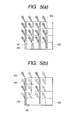
- More specifically, an optical position measurement device is used. The patterns as shown in FIGs. 5(a) and 5(b) are written to measure the positions. The number of the multi beams is also 16 for simplifying the description.
- In a
multi beam area 402 shown in FIGs. 5(a) and 5(b), onbeams 403 are indicated in black and offbeams 404 are indicated in white. When partially using the beams shown in FIG. 5(b), one beam is used for fourunit writing areas 401. Anoblong writing pattern 405 is long as nearly twice the interval of the electron beams. The longer measurement pattern is easily measured. This is a method for using a pattern written at a position closer to the center position of an adjacent electron beam than the center position of its own electron beam. At this time, it is effective to turn off the adjacent electron beam. The number of the electron beams used in writing in parallel is smaller than that of all the beams shown in FIG. 5(a). The optical position measurement has an accuracy higher than that of a typical electron beam position measurement. The position is not measured by its own electron beam to remove the influence of the habit of the writing equipment. These means can be used together with the above-mentioned two means. - Representative construction examples of the present invention will be described below.
- Electron beam writing equipment according to the present invention has: means generating multi electron beams; means on/off controlling each of the multi electron beams according to pattern data that should be written; and means deflection scanning the on/off controlled electron beams together to form desired patterns on a wafer, wherein one side of each of unit writing areas of the multi electron beams is larger than the beam interval of the multi electron beams for writing. One side of the unit writing area is larger than substantially twice the beam interval of the electron beams. One side of the unit writing area is substantially an integral multiple of the beam interval of the electron beams.
- Electron beam writing equipment according to the present invention has: means generating multi electron beams in parallel; means on/off controlling each of the multi electron beams according to pattern data that should be written; and means deflection scanning the on/off controlled multi electron beams together to form desired patterns on a wafer, wherein the center of the unit writing area of the multiple electron beams is shifted for overwriting. The center of the unit writing area is shifted by substantially an integral multiple of the beam interval of the electron beams for writing. The center of the unit writing area is shifted by substantially an integral multiple and substantially 1/integer of the beam interval of the electron beams for writing.
- In the construction of the electron beam writing equipment, in order to detect electron currents of the multi electron beams, a plurality of Faraday cups arrayed corresponding to the multi electron beams are provided to detect variation in the multi electron beams.
- An electron beam writing method according to the present invention has the steps of: on/off controlling each of the multi electron beams according to pattern data that should be written; and deflection scanning the on/off controlled multi electron beams together to form desired patterns on a wafer, wherein the positions of the patterns written with the multi electron beams are measured to obtain relative positions between the multi electron beams to correct the patterns. One side of each of unit writing areas of the multi electron beams is larger than the beam interval of the multi electron beams for writing. The positions of the patterns written with the multi electron beams are measured optically.
- In the electron beam writing method, the position of a pattern written at a position closer to the center position of a second adjacent electron beam than the center position of a first electron beam of the multi electron beams is measured optically so as to correct the pattern.
-
- FIG. 1 is a diagram of assistance in explaining a writing area;
- FIG. 2 is a diagram of assistance in explaining an example of a prior art writing method;
- FIG. 3 is a diagram of assistance in explaining an example of a writing method according to the present invention;
- FIGs. 4(a) and 4(b) are diagrams of assistance in explaining another example of the writing method according to the present invention;
- FIGs. 5(a) and 5(b) are diagrams of assistance in explaining an example of a writing pattern according to the present invention;
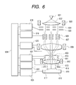
- FIG. 6 is a diagram of assistance in explaining an example of an equipment construction for use in embodiments of the present invention;
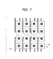
- FIG. 7 is a diagram showing a construction example of Faraday cups;
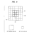
- FIG. 8 is a diagram of assistance in explaining
a writing area of
Embodiment 1 of the present invention; and - FIGs. 9(a) to 9(c) are diagrams of assistance in explaining writing patterns of Embodiment 3 of the present invention.
-
- Preferred embodiments of the present invention will be described below with reference to the drawings.
- FIG. 6 shows an equipment construction for use in this embodiment. An
electron beam 602 emitted from anelectron gun 601 is irradiated onto a plurality of holedaperture arrays 604 throughcondenser lenses 603 to form multi electron beams. The multi electron beams which pass throughaperture arrays 604 form point beams asintermediate images 607 bylens arrays 605, and are then on/off controlled by deflection ofblanker arrays 606. Theintermediate images 607 are projected onto awafer 615 on astage 616 by a lens doublet havingfirst projection lenses 608 andsecond projection lenses 612.Main deflectors 611 andsub-deflectors 613 act on the multi beams in the same manner to perform positioning on thewafer 615. AFaraday cup 617 is provided on thestage 616 to detect an electron current. - In the drawing, the numeral 609 denotes a blanking aperture; the numeral 610, a dynamic focus and astigmatism adjuster; and the numeral 614, an electron detector. The
numerals 618 to 624 show a control system of this equipment construction and denote a focus control circuit, a pattern generating circuit, a lens control circuit, a deflection control circuit, a signal handling circuit, a stage control circuit, and a CPU, respectively. - In FIG. 6, the lens doublet has one stage for simplifying the construction. When increasing the demagnification ratio for high resolution, it is effective that the lens doublets are arrayed in two stages in series.
- FIG. 7 shows an example of the construction of Faraday cups. A plurality of micro Faraday cups 702 electrically isolated to detect electron currents of
multi electron beams 701 via awire 703 at the same time are arrayed in two dimensions. In this example, the number of theelectron beams 701 is 1024 in a 32 × 32 matrix form. This can detect variation in the multi electron beams from the electron currents measured in the plurality of Faraday cups 702. - FIG. 8 shows an example of a writing area. For simplification, only a
unit writing area 803 of four electron beams is shown. The diagonally shaded part surrounded bycenters 801 of the four electron beams is written with the four electron beams. The deflection position in theunit writing area 803 is different. A smoothing effect can be expected. When the unit writing area is triple, writing with nine electron beams is permitted. - In this embodiment, the electron beam interval is 2 µm and the unit writing area is 4 µm square. The unit writing area is increased, which is not a significant problem because the deflection amount is originally small in the multi beam system. From writing to a resist, the sizing accuracy and the positioning accuracy of the prior art writing method are 10nm and 30nm, respectively. According to the present invention, they can be improved to 6nm and 18nm, respectively.
- In this embodiment, using the same equipment as
Embodiment 1, point beams having an interval of 100 µm are formed in theintermediate images 607 and are condensed to 1/50 by the two-stage lens doublet. The interval of the electron beams is 2 µm as inEmbodiment 1. The unit writing area is 2 µm square corresponding to the interval of the electron beams. - In this embodiment, an electron beam center shift method is used. The size of the multi beam area is 64 µm square obtained from 32 × 32 beams. In this embodiment, the multi beam area is shifted by 31 µm in two directions to perform overwriting. This is 30 times + 1/2 times the interval of the electron beams. Because of double writing, the fraction of the shift amount is 1/2 to perform overwriting at different deflection positions where possible. The wafer is written with the two different electron beams and deflection positions.
- As a result of the writing to a resist, while the sizing accuracy and the positioning accuracy of the prior art writing method are 10nm and 30nm, respectively, they can be improved to 8nm and 22nm, respectively. The multi beam area is shifted by 20 .7 µm in two directions to perform overwriting three times. The sizing accuracy and the positioning accuracy can be improved to 7nm and 20nm, respectively.
- FIGs. 9(a) to 9(c) show part of the patterns used in this embodiment. Writing is performed to a resist having a thickness of 0.3 µm to optically measure the positions of the developed results. This can measure variation in the electron beams. The data is fed back to the data control system of the writing equipment to improve the writing accuracy.
- In the current state, an optical measurement device has the highest measurement accuracy. Use of this is effective to improve the accuracy of the equipment. In the multi beam system, the electron current of each of the electron beams is small. It is thus difficult to make the measurement accuracy higher with the electron beam itself. The relative positions between the multi electron beams need not be measured in the prior art, which is a new trial.
- Measurement is performed in a
writing pattern 405 within 2 µm as shown in FIG. 9(a). Aunit writing area 401 given to one beam is small. It is thus difficult to optimize the parameter of optical measurement. A given value is fed back to the equipment control to improve the prior art positioning accuracy from 30nm to 25nm. - A
writing pattern 406 shown in FIG. 9(b) is used. Theunit writing area 401 is 4 µm square to improve the measurement accuracy. The positioning accuracy can be improved to 22nm. In this method, an adjacent electron beam cannot be used at a time. Writing must be done multiple times, which is not a significant problem. Since amulti beam area 402 is small, writing can be made onto the same wafer. - As shown in FIG. 9(c), the area per electron beam is increased to arrange a plurality of writing
patterns 407. The positions of the plurality of writing patterns in theunit writing area 401 can be known. The shapes can be corrected. The shapes are basically common in all the electron beams. They may be different depending on the position due to influence of aberration. Measurement with multi beams is preferable. This is fed back to the data control system of the equipment. - Correction of the shape of the unit writing area is particularly important when using the enlarged unit writing area in
Embodiment 1. Use of a combination thereof is very effective. The positioning accuracy can be improved to 20nm. Using the writing method ofEmbodiment 1 together can improve it to 15nm. - In these embodiments, multi electron beams are formed from a single electron source. The present invention can be executed using a plurality of electron sources. In this case, the number of electron optical elements in a vacuum can be reduced. Variation in the characteristics of the electron sources is the disadvantage.
- As described above, according to the present invention, the writing accuracy in the writing equipment of a multi electron beam system can be improved.
Claims (12)
- Electron beam writing equipment comprising:means generating multi electron beams; means on/off controlling each of said multi electron beams according to pattern data that should be written; and means deflection scanning said on/off controlled electron beams together to form desired patterns on a wafer, wherein one side of the maximum writing area in which each of said multi electron beams can be deflection scanned successively is larger than the beam interval of said multi electron beams for writing.
- The electron beam writing equipment according to claim 1, wherein one side of said writing area is larger than substantially twice the beam interval of said electron beams.
- The electron beam writing equipment according to claim 1, wherein one side of said writing area is substantially an integral multiple of the beam interval of said electron beams.
- The electron beam writing equipment according to claim 1, wherein in order to detect electron currents of said multi electron beams, a plurality of Faraday cups arrayed corresponding to said multi electron beams are provided.
- Electron beam writing equipment comprising:means generating multi electron beams in parallel;means on/off controlling each of said multi electron beams according to pattern data that should be written;and means deflection scanning said on/off controlled multi electron beams together to form desired patterns on a wafer, wherein the center of the maximum writing area in which each of said multi electron beams can be deflection scanned successively is shifted for overwriting.
- The electron beam writing equipment according to claim 5, wherein the center of said writing area is shifted by substantially an integral multiple of the beam interval of said electron beams for writing.
- The electron beam writing equipment according to claim 5, wherein the center of said writing area is shifted by substantially an integral multiple and substantially 1/integer of the beam interval of said electron beams for writing.
- The electron beam writing equipment according to claim 5, wherein in order to measure electron currents of said multi electron beams, a plurality of Faraday cups arrayed corresponding to said multi electron beams are provided to detect variation in said multi electron beams.
- An electron beam writing method comprising the steps of: on/off controlling each of multi electron beams according to pattern data that should be written; and deflection scanning said on/off controlled multi electron beams together to form desired patterns on a wafer, wherein the positions of the patterns written with said multi electron beams are measured to obtain relative positions between said multi electron beams to correct said patterns.
- The electron beam writing method according to claim 9, wherein one side of the maximum writing area in which each of said multi electron beams can be deflection scanned successively is larger than the beam interval of said multi electron beams for writing.
- The electron beam writing method according to claim 9 or 10, wherein the positions of the patterns written with said multi electron beams are measured optically.
- The electron beam writing method according to claim 9, wherein the position of a pattern written at a position closer to the center position of a second adjacent electron beam than the center position of a first electron beam of said multi electron beams is measured optically so as to correct said pattern.
Applications Claiming Priority (2)
| Application Number | Priority Date | Filing Date | Title |
|---|---|---|---|
| JP2002225973 | 2002-08-02 | ||
| JP2002225973A JP4183454B2 (en) | 2002-08-02 | 2002-08-02 | Electron beam drawing device |
Publications (2)
| Publication Number | Publication Date |
|---|---|
| EP1396873A1 true EP1396873A1 (en) | 2004-03-10 |
| EP1396873B1 EP1396873B1 (en) | 2019-05-01 |
Family
ID=31185064
Family Applications (1)
| Application Number | Title | Priority Date | Filing Date |
|---|---|---|---|
| EP03250725.3A Expired - Lifetime EP1396873B1 (en) | 2002-08-02 | 2003-02-05 | Electron beam writing equipment |
Country Status (3)
| Country | Link |
|---|---|
| US (1) | US7015482B2 (en) |
| EP (1) | EP1396873B1 (en) |
| JP (1) | JP4183454B2 (en) |
Cited By (1)
| Publication number | Priority date | Publication date | Assignee | Title |
|---|---|---|---|---|
| TWI506685B (en) * | 2011-02-18 | 2015-11-01 | 紐富來科技股份有限公司 | Charge particle beam rendering device and charged particle beam rendering method |
Families Citing this family (5)
| Publication number | Priority date | Publication date | Assignee | Title |
|---|---|---|---|---|
| GB2408143B (en) * | 2003-10-20 | 2006-11-15 | Ims Nanofabrication Gmbh | Charged-particle multi-beam exposure apparatus |
| US7075093B2 (en) * | 2004-05-12 | 2006-07-11 | Gorski Richard M | Parallel multi-electron beam lithography for IC fabrication with precise X-Y translation |
| JP4907092B2 (en) | 2005-03-01 | 2012-03-28 | 株式会社日立ハイテクノロジーズ | Electron beam drawing apparatus and electron beam drawing method |
| JP6215586B2 (en) * | 2012-11-02 | 2017-10-18 | 株式会社ニューフレアテクノロジー | Multi-charged particle beam writing method and multi-charged particle beam writing apparatus |
| US11651934B2 (en) | 2021-09-30 | 2023-05-16 | Kla Corporation | Systems and methods of creating multiple electron beams |
Family Cites Families (7)
| Publication number | Priority date | Publication date | Assignee | Title |
|---|---|---|---|---|
| JP3647128B2 (en) | 1996-03-04 | 2005-05-11 | キヤノン株式会社 | Electron beam exposure apparatus and exposure method thereof |
| JP3796317B2 (en) | 1996-06-12 | 2006-07-12 | キヤノン株式会社 | Electron beam exposure method and device manufacturing method using the same |
| JP3787417B2 (en) * | 1997-06-11 | 2006-06-21 | キヤノン株式会社 | Electron beam exposure method and electron beam exposure apparatus |
| JP4601146B2 (en) * | 2000-10-03 | 2010-12-22 | 株式会社アドバンテスト | Electron beam exposure system |
| EP1271605A4 (en) * | 2000-11-02 | 2009-09-02 | Ebara Corp | Electron beam apparatus and method for manufacturing semiconductor device comprising the apparatus |
| JP2002353112A (en) * | 2001-05-25 | 2002-12-06 | Riipuru:Kk | Electron beam tilt exposure measuring method and tilt calibration method in electron beam proximity exposure apparatus, and electron beam proximity exposure apparatus |
| US6710361B2 (en) * | 2002-04-23 | 2004-03-23 | International Business Machines Corporation | Multi-beam hybrid solenoid lens electron beam system |
-
2002
- 2002-08-02 JP JP2002225973A patent/JP4183454B2/en not_active Expired - Lifetime
-
2003
- 2003-01-31 US US10/354,959 patent/US7015482B2/en not_active Expired - Lifetime
- 2003-02-05 EP EP03250725.3A patent/EP1396873B1/en not_active Expired - Lifetime
Non-Patent Citations (1)
| Title |
|---|
| No Search * |
Cited By (1)
| Publication number | Priority date | Publication date | Assignee | Title |
|---|---|---|---|---|
| TWI506685B (en) * | 2011-02-18 | 2015-11-01 | 紐富來科技股份有限公司 | Charge particle beam rendering device and charged particle beam rendering method |
Also Published As
| Publication number | Publication date |
|---|---|
| JP2004071690A (en) | 2004-03-04 |
| JP4183454B2 (en) | 2008-11-19 |
| EP1396873B1 (en) | 2019-05-01 |
| US20040021095A1 (en) | 2004-02-05 |
| US7015482B2 (en) | 2006-03-21 |
Similar Documents
| Publication | Publication Date | Title |
|---|---|---|
| EP1351272B1 (en) | Electron beam exposure method | |
| JP2019204694A (en) | Multiple electron beam image acquisition device and positioning method of multiple electron beam optical system | |
| JP2017083301A (en) | Pattern inspection method and pattern inspection device | |
| US9916962B2 (en) | Multi charged particle beam irradiation apparatus, multi charged particle beam irradiation method, and multi charged particle beam adjustment method | |
| JPH113845A (en) | Electron beam exposure method and electron beam exposure apparatus | |
| US12046445B2 (en) | Electron beam inspection apparatus and electron beam inspection method | |
| JP6128744B2 (en) | Drawing apparatus, drawing method, and article manufacturing method | |
| US12205272B2 (en) | Pattern inspection device and pattern inspection method | |
| CN117981038A (en) | Multi-electron beam image acquisition device and multi-electron beam image acquisition method | |
| US8008631B2 (en) | Method of acquiring offset deflection amount for shaped beam and lithography apparatus | |
| JP7547082B2 (en) | Pattern inspection device and pattern inspection method | |
| JPH09320931A (en) | Imaging characteristic measuring method and transfer apparatus using the method | |
| EP1396873B1 (en) | Electron beam writing equipment | |
| US6433347B1 (en) | Charged-particle-beam projection-exposure methods and apparatus that selectively expose desired exposure units of a reticle pattern | |
| JP2006086182A (en) | Electron beam drawing method and electron beam drawing apparatus | |
| US20150131075A1 (en) | Drawing apparatus, and method of manufacturing article | |
| JP4477436B2 (en) | Charged particle beam exposure system | |
| JP2001052989A (en) | Charged particle beam exposure method, charged particle beam exposure apparatus and device manufacturing method | |
| JP2005032837A (en) | Charged particle drawing method and device manufacturing method using the method | |
| US7119348B2 (en) | Charged beam writing apparatus and writing method | |
| JPH09330870A (en) | Electron beam exposure apparatus and exposure method thereof | |
| WO2022102266A1 (en) | Image correction device, pattern inspection device and image correction method | |
| US20150129779A1 (en) | Drawing apparatus, and method of manufacturing article | |
| US20140162191A1 (en) | Drawing apparatus, and method of manufacturing article | |
| JP2000124116A (en) | Charged beam exposure method and charged beam exposure apparatus |
Legal Events
| Date | Code | Title | Description |
|---|---|---|---|
| PUAI | Public reference made under article 153(3) epc to a published international application that has entered the european phase |
Free format text: ORIGINAL CODE: 0009012 |
|
| AK | Designated contracting states |
Kind code of ref document: A1 Designated state(s): AT BE BG CH CY CZ DE DK EE ES FI FR GB GR HU IE IT LI LU MC NL PT SE SI SK TR |
|
| AX | Request for extension of the european patent |
Extension state: AL LT LV MK RO |
|
| 17P | Request for examination filed |
Effective date: 20040830 |
|
| AKX | Designation fees paid |
Designated state(s): DE GB NL |
|
| RAP1 | Party data changed (applicant data changed or rights of an application transferred) |
Owner name: HITACHI, LTD. Owner name: CANON KABUSHIKI KAISHA |
|
| 17Q | First examination report despatched |
Effective date: 20090507 |
|
| GRAP | Despatch of communication of intention to grant a patent |
Free format text: ORIGINAL CODE: EPIDOSNIGR1 |
|
| RIC1 | Information provided on ipc code assigned before grant |
Ipc: H01J 37/304 19800101ALI20180806BHEP Ipc: H01J 37/317 19800101AFI20180806BHEP Ipc: B82Y 10/00 20110101ALI20180806BHEP Ipc: B82Y 40/00 20110101ALI20180806BHEP Ipc: H01J 37/30 19680901ALI20180806BHEP |
|
| INTG | Intention to grant announced |
Effective date: 20180910 |
|
| RIN1 | Information on inventor provided before grant (corrected) |
Inventor name: NAKAYAMA, YOSHINORI, C/O HITACHI, LTD., IP GROUP Inventor name: MURAKI, MASATO Inventor name: KAMIMURA, OSAMU, C/O HITACHI, LTD., IP GROUP Inventor name: TAKAKUMA, MASAKI Inventor name: SOHDA, YASUNARI, C/O HITACHI, LTD., IP GROUP |
|
| GRAJ | Information related to disapproval of communication of intention to grant by the applicant or resumption of examination proceedings by the epo deleted |
Free format text: ORIGINAL CODE: EPIDOSDIGR1 |
|
| RIC1 | Information provided on ipc code assigned before grant |
Ipc: H01J 37/304 20060101ALI20180806BHEP Ipc: B82Y 40/00 20110101ALI20180806BHEP Ipc: H01J 37/30 20060101ALI20180806BHEP Ipc: B82Y 10/00 20110101ALI20180806BHEP Ipc: H01J 37/317 20060101AFI20180806BHEP |
|
| INTC | Intention to grant announced (deleted) | ||
| GRAJ | Information related to disapproval of communication of intention to grant by the applicant or resumption of examination proceedings by the epo deleted |
Free format text: ORIGINAL CODE: EPIDOSDIGR1 |
|
| GRAR | Information related to intention to grant a patent recorded |
Free format text: ORIGINAL CODE: EPIDOSNIGR71 |
|
| GRAS | Grant fee paid |
Free format text: ORIGINAL CODE: EPIDOSNIGR3 |
|
| GRAA | (expected) grant |
Free format text: ORIGINAL CODE: 0009210 |
|
| AK | Designated contracting states |
Kind code of ref document: B1 Designated state(s): DE GB NL |
|
| INTG | Intention to grant announced |
Effective date: 20190325 |
|
| REG | Reference to a national code |
Ref country code: GB Ref legal event code: FG4D |
|
| RIN1 | Information on inventor provided before grant (corrected) |
Inventor name: NAKAYAMA, YOSHINORI Inventor name: SOHDA, YASUNARI Inventor name: KAMIMURA, OSAMU Inventor name: TAKAKUWA, MASAKI Inventor name: MURAKI, MASATO |
|
| REG | Reference to a national code |
Ref country code: DE Ref legal event code: R096 Ref document number: 60351972 Country of ref document: DE |
|
| REG | Reference to a national code |
Ref country code: NL Ref legal event code: FP |
|
| REG | Reference to a national code |
Ref country code: DE Ref legal event code: R097 Ref document number: 60351972 Country of ref document: DE |
|
| PLBE | No opposition filed within time limit |
Free format text: ORIGINAL CODE: 0009261 |
|
| STAA | Information on the status of an ep patent application or granted ep patent |
Free format text: STATUS: NO OPPOSITION FILED WITHIN TIME LIMIT |
|
| 26N | No opposition filed |
Effective date: 20200204 |
|
| PGFP | Annual fee paid to national office [announced via postgrant information from national office to epo] |
Ref country code: GB Payment date: 20200203 Year of fee payment: 18 Ref country code: NL Payment date: 20200123 Year of fee payment: 18 Ref country code: DE Payment date: 20200122 Year of fee payment: 18 |
|
| REG | Reference to a national code |
Ref country code: DE Ref legal event code: R119 Ref document number: 60351972 Country of ref document: DE |
|
| GBPC | Gb: european patent ceased through non-payment of renewal fee |
Effective date: 20210205 |
|
| REG | Reference to a national code |
Ref country code: NL Ref legal event code: MM Effective date: 20210301 |
|
| PG25 | Lapsed in a contracting state [announced via postgrant information from national office to epo] |
Ref country code: NL Free format text: LAPSE BECAUSE OF NON-PAYMENT OF DUE FEES Effective date: 20210301 |
|
| PG25 | Lapsed in a contracting state [announced via postgrant information from national office to epo] |
Ref country code: DE Free format text: LAPSE BECAUSE OF NON-PAYMENT OF DUE FEES Effective date: 20210901 Ref country code: GB Free format text: LAPSE BECAUSE OF NON-PAYMENT OF DUE FEES Effective date: 20210205 |