EP1396174B1 - Galvanically isolated delivery of power to high voltage circuit parts - Google Patents
Galvanically isolated delivery of power to high voltage circuit parts Download PDFInfo
- Publication number
- EP1396174B1 EP1396174B1 EP02732945A EP02732945A EP1396174B1 EP 1396174 B1 EP1396174 B1 EP 1396174B1 EP 02732945 A EP02732945 A EP 02732945A EP 02732945 A EP02732945 A EP 02732945A EP 1396174 B1 EP1396174 B1 EP 1396174B1
- Authority
- EP
- European Patent Office
- Prior art keywords
- high voltage
- wall
- inserts
- voltage apparatus
- conductive
- Prior art date
- Legal status (The legal status is an assumption and is not a legal conclusion. Google has not performed a legal analysis and makes no representation as to the accuracy of the status listed.)
- Expired - Lifetime
Links
- 238000000576 coating method Methods 0.000 claims description 22
- 239000011248 coating agent Substances 0.000 claims description 20
- 239000003990 capacitor Substances 0.000 claims description 7
- PXHVJJICTQNCMI-UHFFFAOYSA-N Nickel Chemical compound [Ni] PXHVJJICTQNCMI-UHFFFAOYSA-N 0.000 claims description 6
- 229910052759 nickel Inorganic materials 0.000 claims description 3
- 230000007704 transition Effects 0.000 claims description 2
- 230000007246 mechanism Effects 0.000 description 9
- 230000008878 coupling Effects 0.000 description 7
- 238000010168 coupling process Methods 0.000 description 7
- 238000005859 coupling reaction Methods 0.000 description 7
- 238000004804 winding Methods 0.000 description 6
- 239000000463 material Substances 0.000 description 4
- 239000004033 plastic Substances 0.000 description 4
- 229920003023 plastic Polymers 0.000 description 4
- 239000004020 conductor Substances 0.000 description 3
- 239000000835 fiber Substances 0.000 description 3
- 239000012811 non-conductive material Substances 0.000 description 3
- 239000003822 epoxy resin Substances 0.000 description 2
- 229920000647 polyepoxide Polymers 0.000 description 2
- 229910001369 Brass Inorganic materials 0.000 description 1
- 230000008901 benefit Effects 0.000 description 1
- 239000010951 brass Substances 0.000 description 1
- 239000012530 fluid Substances 0.000 description 1
- 230000017525 heat dissipation Effects 0.000 description 1
- 238000010438 heat treatment Methods 0.000 description 1
- 238000009413 insulation Methods 0.000 description 1
- 238000000034 method Methods 0.000 description 1
- 238000012986 modification Methods 0.000 description 1
- 230000004048 modification Effects 0.000 description 1
- 230000003287 optical effect Effects 0.000 description 1
- 230000001681 protective effect Effects 0.000 description 1
- 230000001960 triggered effect Effects 0.000 description 1
- 238000003466 welding Methods 0.000 description 1
Images


Classifications
-
- H—ELECTRICITY
- H03—ELECTRONIC CIRCUITRY
- H03K—PULSE TECHNIQUE
- H03K3/00—Circuits for generating electric pulses; Monostable, bistable or multistable circuits
- H03K3/02—Generators characterised by the type of circuit or by the means used for producing pulses
- H03K3/53—Generators characterised by the type of circuit or by the means used for producing pulses by the use of an energy-accumulating element discharged through the load by a switching device controlled by an external signal and not incorporating positive feedback
- H03K3/57—Generators characterised by the type of circuit or by the means used for producing pulses by the use of an energy-accumulating element discharged through the load by a switching device controlled by an external signal and not incorporating positive feedback the switching device being a semiconductor device
-
- H—ELECTRICITY
- H05—ELECTRIC TECHNIQUES NOT OTHERWISE PROVIDED FOR
- H05B—ELECTRIC HEATING; ELECTRIC LIGHT SOURCES NOT OTHERWISE PROVIDED FOR; CIRCUIT ARRANGEMENTS FOR ELECTRIC LIGHT SOURCES, IN GENERAL
- H05B6/00—Heating by electric, magnetic or electromagnetic fields
- H05B6/64—Heating using microwaves
Definitions
- This invention relates to the delivery of power to high voltage devices, and in particular to the delivering of It power to eht devices, for example to power control circuitry.
- GB 9928074.5 and GB 9928049.7 describe a pulsed switching apparatus for an eht load such as a magnetron.
- a stack of FET switch modules are arranged in an oil filled chamber surrounded by four capacitors which are mounted within a plastics housing.
- the switch stack receives a eht supply, typically at about - 55kV and delivers a series of eht pulses to the magnetron.
- the switch also includes various control circuitry which operates at It voltages. This circuitry controls functions such as triggering of the FET switches.
- the invention aims to overcome this problem and in its broadest form delivers power by magnetic coupling across a wall of a housing.
- a high voltage apparatus comprising a means for delivering high voltages to a load, and a housing in which the high voltage delivery means is arranged, wherein the housing includes a plurality of walls, one of which is non-conductive and includes a transformer for delivering a low voltage supply to a switch system, the transformer having a primary coil and core arranged in a first insert on a first side of the wall and a secondary coil and core arranged in a second insert on a second side of the wall, whereby power can be magnetically coupled across the wall, and wherein the first and second inserts have a conductive coating formed on the surfaces thereof and are arranged between the first side of the wall and the primary coil and core, and the second side of the wall and the secondary coil and core, and wherein the inserts are shaped to minimise electric stresses.
- Embodiments of the invention have the advantage that It power can be delivered to devices that are at an eht potential.
- the use of magnetic coupling across a non conductive wall of the housing, preferably an end wall, avoids the need for seals, gaskets and the like which can give rise to oil leaks and which are generally unsatisfactory.
- the conductive coating helps to dissipate electric stresses and enables relatively non-precision components to be used, for example, standard transformer cores which have sharp edges which would otherwise generate unacceptable electric stresses.
- the inserts are arranged snugly in chambers on either side of the wall.
- the use of inserts is a convenient way of introducing the coating into the wall.
- the inserts are annular and have a smooth concave outer surface with a flat face on which the conductive coating is deposited. This arrangement helps to minimise electric stresses.
- the conductive coating may extend over the side wall of the inserts.
- the inserts have a chamber in which the coil and core are received.
- the coil and core are therefore spaced apart from the conductive coating by the thickness of a bottom wall of the inserts.
- Figures 1 and 2 show the switching mechanism disclosed in our earlier applications GB9928074.5 and GB9928049.7.
- the mechanism provides high voltage pulses to a high voltage load, such as a magnetron, by switching a capacitance.
- the switching is triggered by trigger pulses derived from a high voltage supply and the capacitance is also charged by that supply.
- the switching arrangement shown in Figures 1 and 2 comprises a switch stack arranged within a chamber surrounded by a plurality of capacitances.
- the switch stack comprises a number of FET modules 1, 2, 3, 4,...n, each of which includes one or more FET switches. There may be, for example, 75 FET modules in the stack and each module may include three FET switches.
- the modules are mounted in close proximity to one another and are stacked along the axis in Figure 1.
- each module includes a secondary transformer winding 6 with a common primary winding 7 extending along the length of the axis to act as the primary for each module. The primary is used to provide power and drive pulses to the FET switches.
- Power to the switching arrangement is applied from a source 8 to a trigger driver 9 at the high voltage end of the stack which is maintained at -55kV.
- the trigger driver is formed as a module of similar dimensions to the FET modules and forms the end module of the stack.
- the load 10 for example a magnetron, is connected to an output 11 of the switching mechanism to receive pulses from the switching mechanism.
- the output 11 also provides an output 12 to a heater transformer for heating the magnetron cathode.
- the power for the transformer is provided from a power source 12.
- the switching mechanism is arranged within a housing 14.
- the housing is formed of a non-conductive material such as a plastics material and comprises outer and inner walls 15, 16 defining an annular chamber therebetween, and an interior chamber 23 bounded by the inner walls and in which the switching stack is arranged.
- the annular chamber and the interior chamber 23 communicate via apertures 24, 25 in the inner wall 16.
- the housing and the annular and interior chambers are rectangular in cross section.
- Four capacitors 17, 18, 19, 20 are arranged in the annular chamber, one on each side, and extend along the length of the chamber shielding the switching mechanism.
- the capacitors are connected at the high voltage end to the first switch module and to the load 10 at the low voltage end, which may be at ground.
- the capacitors each comprise a plurality of parallel plates forming capacitor elements which are interconnected so that a nominally linear voltage gradient appears from the power supply end to the zero volt end.
- the capacitors may each be 0.15 ⁇ f.
- the unit is oil filled for heat dissipation and insulation. Oil can pass between the annular and inner chambers through passageways 24, 25.
- An expansion tank 26 is connected to the chambers which includes a diaphragm, and which moves with the changes in oil volume, for example due to temperature changes.
- the switching stack also comprises a control module 40 which is mounted on the stack between the trigger power supply module and the first FET module 1 and which is of similar dimensions to the FET modules.
- the control module controls triggering of the FET switches and floats at the high voltage of -55kV but requires its own It power supply to operate the control circuitry. It will be appreciated from Figures 1 and 2 that there is very limited space for the necessary transformer to provide that power supply and, also, a need tb isolate the LT voltage from the -55kv supply.
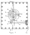
- Figures 3 to 6 illustrate an end plate 41 of the casing.
- the end plate 41 is fixed to the casing at the high voltage end by any convenient method such as welding to close the annular and interior chambers.
- the end plate is made from a non-conductive material, preferably a plastics material such as epoxy resin.
- the high voltage power supply is provided to the interior chamber 23 through a side wall 42 of the end plate 41.
- a circular screw fixing 44 is provided to receive a threaded coaxial connector.
- An interior passageway 45 extends through the end plate to an anchor plate 46 which includes a socket 48 into which the central conductor of a coaxial power cable is received.
- the anchor plate which is of a convenient conductive material such as brass, is accessible on the inside face of the end plate by which the power supply can be connected to the trigger driver 9. In Figure 4, the passageway 45 is omitted for clarity.
- each projection 50, 52 includes an annular chamber 54, 56 in which is received an annular insert 58, 60 shown in Figures 7 and 8.
- the annular chambers 54 and 56 are spaced apart and are separated by a thin wall portion 62 of the end plate, (Fig 4). This may typically be 8mm in diameter.
- the two annular chambers are coaxial but offset from the centre of the plate and are not coaxial with the two projections 50, 52.
- the projections each have two pairs of two apertures 64 through which fibre optic cables can be introduced into the interior chamber 26. Fibre optic couplings using fibre optic rods may be moulded in to deliver optical triggering to the FET switches to remove the need for oil/fluid tight seals which are prone to leak.
- annular chambers 54, 56 each have a concave rounded side wall 64 which is smooth over its surface with no sharp edges and is shaped to receive the annular inserts 58, 60 snugly.
- the annular inserts 58, 60 each have a generally flat face 66 which, when in position in the end plate oppose one another.
- the faces 66 at least, are covered with a conductive coating, preferably a nickel film.
- a conductive coating preferably a nickel film.
- the whole or the outer surface of the annular inserts may be covered in the conductive coating.
- the outer wall of the inserts are convex and follow the shape of the inner wall of the annular chambers of the end plate. In position on the end wall, the inserts are coaxial and the conductive coatings, substantially parallel on the end faces.
- the annular inserts are formed of a non-conductive material and, for example, may be mounded from a plastics material such as an epoxy resin.
- Each annular insert has a cylindrical chamber 70 which receives a primary or secondary transformer winding and corc (Fig 7), with the primary winding and core on the outside of the end plate and the secondary winding and core on the inside.
- LT power can then be supplied to the switch mechanism, which is at -55kv, by magnetic coupling across the end plate despite the poor conductivity of the end plate.
- Each of the inserts includes a pair of threaded inserts 72 which may be used to fasten a protective cover to retain the respective transformer winding.
- the embodiment described allows power to be supplied to the switching stack, for example, to operate control circuitry.
- the power supplied is in the order of 100W.
- the power can be supplied to circuitry that is floating at the -55kV potential of the high voltage source.
- the magnetically coupled inserts are not subject to unacceptable levels of electric stresses.
- the annular elements are used as a convenient way of introducing a conductive surface between the respective transformer cores and the wall of the end plate.
- the bottom surface of the annular inserts is flat ensuring that the conductive surfaces are normal to the axis of the cores.
- the conductor chosen for the coating is also magnetic. Nickel based is a preferred material for the coating.
- the conductive coating is not essential and could be omitted, in which case there is no need for the annular inserts. However, if omitted, all the components of the magnetic coupling would require very careful design to ensure that there are no sharp edges which could give rise to high electrical stresses at the high voltages at which the system operates. Such an arrangement, while possible is undesirable as it would be expensive requiring the design of very high precision components, particularly the transformer cores.
- the use of a conductive coating enables cheap, off the shelf transformer cores to be used whose shape would normally give rise to unacceptable electric stresses which the conductive coating can dissipate.
Landscapes
- Physics & Mathematics (AREA)
- Electromagnetism (AREA)
- Constitution Of High-Frequency Heating (AREA)
- Generation Of Surge Voltage And Current (AREA)
- Dc-Dc Converters (AREA)
Description
Claims (14)
- A high voltage apparatus comprising a means for delivering high voltages to a load, and a housing in which the high voltage delivery means is arranged, wherein the housing includes a plurality of walls, one of which is non-conductive and includes a transformer for delivering a low voltage supply to a switch system, the transformer having a primary coil and core arranged in a first insert on a first side of the wall and a secondary coil and core arranged in a second insert on a second side of the wall, whereby power can be magnetically coupled across the wall, and wherein the first and second inserts have a conductive coating formed on the surfaces thereof and are arranged between the first side of the wall and the primary coil and core, and the second side of the wall and the secondary coil and core, and wherein the inserts are shaped to minimise electric stresses.
- A high voltage apparatus according to claim 1, wherein the inserts are annular.
- A high voltage apparatus according to claim 1 or 2, wherein the primary coil and core are arranged on the outside of the non-conductive wall and the secondary coil and core are arranged on the inside of the non-conductive wall.
- A high voltage apparatus according to any preceding claim, wherein the non-conductive wall is an end wall of the housing.
- A high voltage apparatus according to claim 4, wherein the inserts are received snugly in respective chambers in either side of the non-conductive wall.
- A high voltage apparatus according to claim 4 or 5, wherein the first and second inserts each include a chamber for receiving a respective one of the first and second coil and core.
- A high voltage apparatus according to any preceding claim, wherein the inserts have a flat face on which the conductive coating is formed and a concave side wall, the transition between the side wall and the flat face being smooth.
- A high voltage apparatus according to claim 7, wherein the conductive coatings on the flat faces are substantially parallel.
- A high voltage apparatus according to claim 7 or 8, wherein the inserts are coaxial.
- A high voltage apparatus according to claim 7, 8 or 9, wherein the conductive coating extends over the side wall.
- A high voltage apparatus according to any preceding claim, wherein the conductive coating is magnetic.
- A high voltage apparatus according to claim 11, wherein the conductive coating includes nickel.
- A high voltage apparatus according to any preceding claim, wherein the apparatus is a switching apparatus and the high voltage delivery means is a switching stack.
- A high voltage apparatus according to claim 13, wherein the switching stack is coupled to a capacitor for delivering high voltage pulses to the load.
Applications Claiming Priority (3)
| Application Number | Priority Date | Filing Date | Title |
|---|---|---|---|
| GB0114676 | 2001-06-15 | ||
| GB0114676A GB2377822A (en) | 2001-06-15 | 2001-06-15 | Transformer arrangement for delivering low voltage power to a high voltage device |
| PCT/GB2002/002729 WO2002104076A1 (en) | 2001-06-15 | 2002-06-14 | Galvanically isolated delivery of power to high voltage circuits parts |
Publications (2)
| Publication Number | Publication Date |
|---|---|
| EP1396174A1 EP1396174A1 (en) | 2004-03-10 |
| EP1396174B1 true EP1396174B1 (en) | 2004-10-13 |
Family
ID=9916707
Family Applications (1)
| Application Number | Title | Priority Date | Filing Date |
|---|---|---|---|
| EP02732945A Expired - Lifetime EP1396174B1 (en) | 2001-06-15 | 2002-06-14 | Galvanically isolated delivery of power to high voltage circuit parts |
Country Status (6)
| Country | Link |
|---|---|
| US (1) | US7221558B2 (en) |
| EP (1) | EP1396174B1 (en) |
| JP (1) | JP4044037B2 (en) |
| DE (1) | DE60201603T2 (en) |
| GB (1) | GB2377822A (en) |
| WO (1) | WO2002104076A1 (en) |
Families Citing this family (3)
| Publication number | Priority date | Publication date | Assignee | Title |
|---|---|---|---|---|
| US9046577B2 (en) * | 2011-04-13 | 2015-06-02 | GM Global Technology Operations LLC | Corona and partial discharge diagnostic device and method for using the same |
| DE102011120526B3 (en) * | 2011-10-24 | 2013-02-28 | Maschinenfabrik Reinhausen Gmbh | High voltage switching device with power supply device |
| CN107294418B (en) * | 2017-06-29 | 2023-10-03 | 中国工程物理研究院电子工程研究所 | Integrated multipath high-power high-voltage pulse generating device |
Family Cites Families (24)
| Publication number | Priority date | Publication date | Assignee | Title |
|---|---|---|---|---|
| GB499037A (en) * | 1937-07-19 | 1939-01-18 | Alfred Graham & Co Ltd | A system for the transmission of electrical energy to or from a submerged body |
| US3376523A (en) * | 1966-12-27 | 1968-04-02 | Univ California | Transient-suppressing magnetic transmission line |
| FR2061547B1 (en) | 1969-06-03 | 1973-12-21 | Fr | |
| CH538756A (en) | 1971-11-20 | 1973-06-30 | Flako Ag | Dispersion transformer with ferrite core |
| FR2424617A1 (en) | 1978-04-28 | 1979-11-23 | Elliott Brothers London Ltd | INDUCTIVE COUPLERS |
| US4481423A (en) * | 1981-12-10 | 1984-11-06 | Westinghouse Electric Corp. | Assembly for optical communication between high and low voltage component housings |
| US4471440A (en) * | 1982-02-01 | 1984-09-11 | Pitney Bowes Inc. | Electronic postage meter having power magnetically coupled to the meter from the meter base |
| DE8322540U1 (en) * | 1983-08-04 | 1984-10-11 | Siemens AG, 1000 Berlin und 8000 München | SMALL TRANSFORMER |
| DE3700488A1 (en) | 1987-01-08 | 1988-07-21 | Klaus Dipl Ing Becker | Power transformer having a ferromagnetic core |
| CA1309752C (en) * | 1987-05-14 | 1992-11-03 | Kimiaki Yamaguchi | Stationary induction apparatus |
| GB9011970D0 (en) * | 1990-05-29 | 1990-07-18 | Leigh Stewart Prod | Electrical control system for,for example,an air spa bath |
| EP0508521A1 (en) | 1991-04-09 | 1992-10-14 | Koninklijke Philips Electronics N.V. | Transformer |
| US5301096A (en) * | 1991-09-27 | 1994-04-05 | Electric Power Research Institute | Submersible contactless power delivery system |
| CN1050242C (en) * | 1993-06-14 | 2000-03-08 | Vlt公司 | Power converter configuration, control, and construction |
| JP3409145B2 (en) * | 1993-07-26 | 2003-05-26 | 任天堂株式会社 | Small electrical equipment |
| JP3456093B2 (en) * | 1996-06-25 | 2003-10-14 | 松下電工株式会社 | Non-contact power transmission device |
| US6054780A (en) * | 1997-10-23 | 2000-04-25 | Analog Devices, Inc. | Magnetically coupled signal isolator using a Faraday shielded MR or GMR receiving element |
| JP2000078763A (en) * | 1998-09-01 | 2000-03-14 | Matsushita Electric Ind Co Ltd | Contactless charging device |
| JP3743193B2 (en) * | 1999-02-23 | 2006-02-08 | 松下電工株式会社 | Non-contact power transmission device |
| GB2356752B (en) * | 1999-11-29 | 2004-08-11 | Eev Ltd | Switching arrangements |
| GB2356753B (en) | 1999-11-29 | 2004-08-11 | Eev Ltd | Switching arrangement |
| WO2001056045A1 (en) | 2000-01-27 | 2001-08-02 | Koninklijke Philips Electronics N.V. | Transformer having insulation means formed by a mounting plate suitable for a printed circuit |
| US6301128B1 (en) * | 2000-02-09 | 2001-10-09 | Delta Electronics, Inc. | Contactless electrical energy transmission system |
| DE60139512D1 (en) * | 2000-02-24 | 2009-09-17 | Panasonic Elec Works Co Ltd | Contactless power transmission system with function for keeping the load voltage constant |
-
2001
- 2001-06-15 GB GB0114676A patent/GB2377822A/en not_active Withdrawn
-
2002
- 2002-06-14 EP EP02732945A patent/EP1396174B1/en not_active Expired - Lifetime
- 2002-06-14 US US10/480,528 patent/US7221558B2/en not_active Expired - Lifetime
- 2002-06-14 WO PCT/GB2002/002729 patent/WO2002104076A1/en not_active Ceased
- 2002-06-14 DE DE60201603T patent/DE60201603T2/en not_active Expired - Lifetime
- 2002-06-14 JP JP2003506245A patent/JP4044037B2/en not_active Expired - Fee Related
Also Published As
| Publication number | Publication date |
|---|---|
| DE60201603D1 (en) | 2004-11-18 |
| EP1396174A1 (en) | 2004-03-10 |
| US20040190231A1 (en) | 2004-09-30 |
| DE60201603T2 (en) | 2006-02-16 |
| WO2002104076A1 (en) | 2002-12-27 |
| GB0114676D0 (en) | 2001-08-08 |
| JP4044037B2 (en) | 2008-02-06 |
| GB2377822A (en) | 2003-01-22 |
| JP2004532599A (en) | 2004-10-21 |
| US7221558B2 (en) | 2007-05-22 |
Similar Documents
| Publication | Publication Date | Title |
|---|---|---|
| US7256637B2 (en) | High voltage switching apparatus | |
| US4692727A (en) | Dielectric resonator device | |
| US5434353A (en) | Self-supporting insulated conductor arrangement suitable for arrangement in a vacuum container | |
| EP1873560B1 (en) | Lens with adjustable focal length | |
| CN101192741A (en) | Ionization device | |
| WO2009012867A2 (en) | Plasma supply device | |
| KR20060035635A (en) | Method and apparatus for cooling magnetic circuit elements | |
| US7221558B2 (en) | Galvanically isolated delivery of power to high voltage circuits parts | |
| DK0499201T3 (en) | Coil for conditioning a conductor | |
| KR100660307B1 (en) | Modular support for high voltage power supply unit | |
| KR20250135858A (en) | X-ray generator and X-ray imaging device | |
| KR20250135857A (en) | X-ray generator and X-ray imaging device | |
| CA1193681A (en) | Transformers | |
| US4481423A (en) | Assembly for optical communication between high and low voltage component housings | |
| JPH07501179A (en) | High voltage insulation disc | |
| EP4141505A1 (en) | Objective | |
| US20260070819A1 (en) | Water treatment device with simple configuration that uses electrostatic field | |
| US3527952A (en) | Transmission line assembly for phototransducer | |
| Turner | PLASTICS FOR ATOM SMASHERS | |
| CN119485823A (en) | Electric heating device | |
| JP2004532599A5 (en) | ||
| KR20240092285A (en) | Water treatment device using electrostatic field | |
| US20060186864A1 (en) | High voltage switching apparatus | |
| JPH0716556U (en) | High insulation conduction device | |
| JPS6196642A (en) | Optical signal transmission equipment |
Legal Events
| Date | Code | Title | Description |
|---|---|---|---|
| PUAI | Public reference made under article 153(3) epc to a published international application that has entered the european phase |
Free format text: ORIGINAL CODE: 0009012 |
|
| 17P | Request for examination filed |
Effective date: 20031222 |
|
| AK | Designated contracting states |
Kind code of ref document: A1 Designated state(s): AT BE CH CY DE DK ES FI FR GB GR IE IT LI LU MC NL PT SE TR |
|
| AX | Request for extension of the european patent |
Extension state: AL LT LV MK RO SI |
|
| GRAP | Despatch of communication of intention to grant a patent |
Free format text: ORIGINAL CODE: EPIDOSNIGR1 |
|
| RBV | Designated contracting states (corrected) |
Designated state(s): DE FR GB SE |
|
| GRAS | Grant fee paid |
Free format text: ORIGINAL CODE: EPIDOSNIGR3 |
|
| GRAA | (expected) grant |
Free format text: ORIGINAL CODE: 0009210 |
|
| AK | Designated contracting states |
Kind code of ref document: B1 Designated state(s): DE FR GB SE |
|
| REG | Reference to a national code |
Ref country code: GB Ref legal event code: FG4D |
|
| RAP2 | Party data changed (patent owner data changed or rights of a patent transferred) |
Owner name: E2V TECHNOLOGIES (UK) LIMITED |
|
| REG | Reference to a national code |
Ref country code: IE Ref legal event code: FG4D |
|
| REF | Corresponds to: |
Ref document number: 60201603 Country of ref document: DE Date of ref document: 20041118 Kind code of ref document: P |
|
| REG | Reference to a national code |
Ref country code: SE Ref legal event code: TRGR |
|
| LTIE | Lt: invalidation of european patent or patent extension |
Effective date: 20041013 |
|
| PLBE | No opposition filed within time limit |
Free format text: ORIGINAL CODE: 0009261 |
|
| STAA | Information on the status of an ep patent application or granted ep patent |
Free format text: STATUS: NO OPPOSITION FILED WITHIN TIME LIMIT |
|
| ET | Fr: translation filed | ||
| 26N | No opposition filed |
Effective date: 20050714 |
|
| REG | Reference to a national code |
Ref country code: FR Ref legal event code: PLFP Year of fee payment: 15 |
|
| REG | Reference to a national code |
Ref country code: FR Ref legal event code: PLFP Year of fee payment: 16 |
|
| REG | Reference to a national code |
Ref country code: DE Ref legal event code: R082 Ref document number: 60201603 Country of ref document: DE Representative=s name: MANITZ FINSTERWALD PATENT- UND RECHTSANWALTSPA, DE Ref country code: DE Ref legal event code: R081 Ref document number: 60201603 Country of ref document: DE Owner name: TELEDYNE UK LTD., CHELMSFORD, GB Free format text: FORMER OWNER: E2V TECHNOLOGIES (UK) LTD., CHELMSFORD, ESSEX, GB Ref country code: DE Ref legal event code: R082 Ref document number: 60201603 Country of ref document: DE Representative=s name: MANITZ FINSTERWALD PATENTANWAELTE PARTMBB, DE Ref country code: DE Ref legal event code: R081 Ref document number: 60201603 Country of ref document: DE Owner name: TELEDYNE E2V (UK) LTD., CHELMSFORD, GB Free format text: FORMER OWNER: E2V TECHNOLOGIES (UK) LTD., CHELMSFORD, ESSEX, GB |
|
| REG | Reference to a national code |
Ref country code: FR Ref legal event code: CD Owner name: TELEDYNE E2V (UK) LIMITED, GB Effective date: 20180410 |
|
| REG | Reference to a national code |
Ref country code: FR Ref legal event code: PLFP Year of fee payment: 17 |
|
| REG | Reference to a national code |
Ref country code: DE Ref legal event code: R082 Ref document number: 60201603 Country of ref document: DE Representative=s name: MANITZ FINSTERWALD PATENT- UND RECHTSANWALTSPA, DE Ref country code: DE Ref legal event code: R081 Ref document number: 60201603 Country of ref document: DE Owner name: TELEDYNE UK LTD., CHELMSFORD, GB Free format text: FORMER OWNER: TELEDYNE E2V (UK) LTD., CHELMSFORD, ESSEX, GB |
|
| PGFP | Annual fee paid to national office [announced via postgrant information from national office to epo] |
Ref country code: FR Payment date: 20200625 Year of fee payment: 19 Ref country code: DE Payment date: 20200629 Year of fee payment: 19 |
|
| PGFP | Annual fee paid to national office [announced via postgrant information from national office to epo] |
Ref country code: GB Payment date: 20200629 Year of fee payment: 19 Ref country code: SE Payment date: 20200629 Year of fee payment: 19 |
|
| REG | Reference to a national code |
Ref country code: DE Ref legal event code: R119 Ref document number: 60201603 Country of ref document: DE |
|
| REG | Reference to a national code |
Ref country code: SE Ref legal event code: EUG |
|
| GBPC | Gb: european patent ceased through non-payment of renewal fee |
Effective date: 20210614 |
|
| PG25 | Lapsed in a contracting state [announced via postgrant information from national office to epo] |
Ref country code: GB Free format text: LAPSE BECAUSE OF NON-PAYMENT OF DUE FEES Effective date: 20210614 Ref country code: DE Free format text: LAPSE BECAUSE OF NON-PAYMENT OF DUE FEES Effective date: 20220101 |
|
| PG25 | Lapsed in a contracting state [announced via postgrant information from national office to epo] |
Ref country code: SE Free format text: LAPSE BECAUSE OF NON-PAYMENT OF DUE FEES Effective date: 20210615 Ref country code: FR Free format text: LAPSE BECAUSE OF NON-PAYMENT OF DUE FEES Effective date: 20210630 |