EP1394849A1 - Cluster tool and method for controlling transport - Google Patents
Cluster tool and method for controlling transport Download PDFInfo
- Publication number
- EP1394849A1 EP1394849A1 EP02707288A EP02707288A EP1394849A1 EP 1394849 A1 EP1394849 A1 EP 1394849A1 EP 02707288 A EP02707288 A EP 02707288A EP 02707288 A EP02707288 A EP 02707288A EP 1394849 A1 EP1394849 A1 EP 1394849A1
- Authority
- EP
- European Patent Office
- Prior art keywords
- load lock
- processed
- wafer
- transfer
- period
- Prior art date
- Legal status (The legal status is an assumption and is not a legal conclusion. Google has not performed a legal analysis and makes no representation as to the accuracy of the status listed.)
- Granted
Links
Images


Classifications
-
- H—ELECTRICITY
- H10—SEMICONDUCTOR DEVICES; ELECTRIC SOLID-STATE DEVICES NOT OTHERWISE PROVIDED FOR
- H10P—GENERIC PROCESSES OR APPARATUS FOR THE MANUFACTURE OR TREATMENT OF DEVICES COVERED BY CLASS H10
- H10P72/00—Handling or holding of wafers, substrates or devices during manufacture or treatment thereof
- H10P72/50—Handling or holding of wafers, substrates or devices during manufacture or treatment thereof for positioning, orientation or alignment
-
- H—ELECTRICITY
- H10—SEMICONDUCTOR DEVICES; ELECTRIC SOLID-STATE DEVICES NOT OTHERWISE PROVIDED FOR
- H10P—GENERIC PROCESSES OR APPARATUS FOR THE MANUFACTURE OR TREATMENT OF DEVICES COVERED BY CLASS H10
- H10P72/00—Handling or holding of wafers, substrates or devices during manufacture or treatment thereof
- H10P72/04—Apparatus for manufacture or treatment
- H10P72/0451—Apparatus for manufacturing or treating in a plurality of work-stations
- H10P72/0461—Apparatus for manufacturing or treating in a plurality of work-stations characterised by the presence of two or more transfer chambers
-
- H—ELECTRICITY
- H10—SEMICONDUCTOR DEVICES; ELECTRIC SOLID-STATE DEVICES NOT OTHERWISE PROVIDED FOR
- H10P—GENERIC PROCESSES OR APPARATUS FOR THE MANUFACTURE OR TREATMENT OF DEVICES COVERED BY CLASS H10
- H10P72/00—Handling or holding of wafers, substrates or devices during manufacture or treatment thereof
- H10P72/04—Apparatus for manufacture or treatment
- H10P72/0451—Apparatus for manufacturing or treating in a plurality of work-stations
- H10P72/0452—Apparatus for manufacturing or treating in a plurality of work-stations characterised by the layout of the process chambers
- H10P72/0454—Apparatus for manufacturing or treating in a plurality of work-stations characterised by the layout of the process chambers surrounding a central transfer chamber
-
- H—ELECTRICITY
- H10—SEMICONDUCTOR DEVICES; ELECTRIC SOLID-STATE DEVICES NOT OTHERWISE PROVIDED FOR
- H10P—GENERIC PROCESSES OR APPARATUS FOR THE MANUFACTURE OR TREATMENT OF DEVICES COVERED BY CLASS H10
- H10P72/00—Handling or holding of wafers, substrates or devices during manufacture or treatment thereof
- H10P72/06—Apparatus for monitoring, sorting, marking, testing or measuring
- H10P72/0612—Production flow monitoring, e.g. for increasing throughput
-
- H—ELECTRICITY
- H10—SEMICONDUCTOR DEVICES; ELECTRIC SOLID-STATE DEVICES NOT OTHERWISE PROVIDED FOR
- H10P—GENERIC PROCESSES OR APPARATUS FOR THE MANUFACTURE OR TREATMENT OF DEVICES COVERED BY CLASS H10
- H10P72/00—Handling or holding of wafers, substrates or devices during manufacture or treatment thereof
- H10P72/30—Handling or holding of wafers, substrates or devices during manufacture or treatment thereof for conveying, e.g. between different workstations
- H10P72/33—Handling or holding of wafers, substrates or devices during manufacture or treatment thereof for conveying, e.g. between different workstations into and out of processing chamber
- H10P72/3304—Handling or holding of wafers, substrates or devices during manufacture or treatment thereof for conveying, e.g. between different workstations into and out of processing chamber characterised by movements or sequence of movements of transfer devices
-
- Y—GENERAL TAGGING OF NEW TECHNOLOGICAL DEVELOPMENTS; GENERAL TAGGING OF CROSS-SECTIONAL TECHNOLOGIES SPANNING OVER SEVERAL SECTIONS OF THE IPC; TECHNICAL SUBJECTS COVERED BY FORMER USPC CROSS-REFERENCE ART COLLECTIONS [XRACs] AND DIGESTS
- Y10—TECHNICAL SUBJECTS COVERED BY FORMER USPC
- Y10S—TECHNICAL SUBJECTS COVERED BY FORMER USPC CROSS-REFERENCE ART COLLECTIONS [XRACs] AND DIGESTS
- Y10S414/00—Material or article handling
- Y10S414/135—Associated with semiconductor wafer handling
- Y10S414/139—Associated with semiconductor wafer handling including wafer charging or discharging means for vacuum chamber
Definitions
- the present invention relates to a cluster tool and a transfer control method.
- processing residual periods for wafers which are being processed at present in process chambers are calculated respectively, and selection of a wafer to be taken out of a load port is made in such a manner that the next wafer is transferred to a process chamber having the shortest processing residual period.
- An object of the present invention is to provide a cluster tool provided with load lock chambers in which transfer delay can be improved and a transfer control method thereof.
- the present invention is characterized by comprising: a plurality of process chambers for performing process processing for objects to be processed; load lock chambers coupled to the process chambers respectively for transferring the objects to be processed to the process chambers; a loader module coupled to the load lock chambers for transferring the objects to be processed to the load lock chambers; and a transfer control unit for selecting an object to be processed that is to be transferred next by the loader module, based on timings for when the load lock chambers get ready to permit transfers of the objects to be processed thereto.
- the transfer control unit comprises: a transfer period calculating unit for calculating a period for each of the load lock chambers to get ready to permit a next transfer thereto, when the object to be processed is transferred into any one of the load lock chambers; and a selecting unit for selecting, as an object to be processed that is to be transferred next, an object to be processed having the shortest period to get ready to be transferable.
- the present invention is characterized by comprising: a plurality of process chambers for performing process processing for objects to be processed; load lock chambers coupled to the process chambers respectively for transferring the objects to be processed to the process chambers; a loader module coupled to the load lock chambers for transferring the objects to be processed to the load lock chambers; and a transfer control unit for selecting an object to be processed that is to be transferred next by the loader module, based on timings for when the process chambers get ready to permit transfers of the objects to be processed thereto.
- the transfer control unit comprises: a transfer period calculating unit for calculating a period for each of the process chambers to get ready to permit a next transfer thereto, when the object to be processed is transferred into any one of the load lock chambers; and a selecting unit for selecting, as an object to be processed that is to be transferred next, an object to be processed having the shortest period to get ready to be transferable.
- the present invention is characterized in that the loader module is provided with a positioning mechanism for positioning the object to be processed, and that the object to be processed that is to be transferred next selected by the transfer control unit is positioned by the positioning mechanism, thereafter transferred to the front of the load lock chamber, and kept waiting.
- a transfer control method of transferring objects to be processed via load lock chambers to a plurality of process chambers is characterized by comprising: selecting an object to be processed that is to be transferred next based on timings for when the load lock chambers get ready to permit transfers of the objects to be processed thereto.
- a transfer control method of transferring objects to be processed via load lock chambers to a plurality of process chambers is characterized by comprising: selecting an object to be processed that is to be transferred next based on timings for when the process chambers get ready to permit transfers of the objects to be processed thereto.
- the present invention is characterized by further comprising: positioning the selected object to be processed that is to be transferred next by a positioning mechanism, thereafter transferring the object to the front of the load lock chamber, and keeping the object waiting.
- FIG. 1 is a cross-sectional view showing a schematic configuration of a cluster tool according to an embodiment of the present invention.
- load ports LP1 to LP3 which accommodate wafers W
- a transfer chamber TR in which the wafers W are transferred and an orienter OR which positions the wafers W
- cassettes or FOUPs CS1 to CS3 which accommodate unprocessed wafers W and processed wafers W, are located.
- load ports LP1 to LP3 can also be set as ports for dummy wafers in which cassettes or the like accommodating dummy wafers are located.
- the orienter OR is coupled, process ships PS1 and PS2 are coupled via load lock doors LG1 and LG2, and further the load ports LP1 to LP3 are coupled via load port doors CG1 to CG3.
- loader arms LA1 and LA2 in a two-tier structure are provided, and the loader arms LA1 and LA2 perform transfers of wafers W among the load ports LP1 to LP3, load lock chambers LL1 and LL2, and the orienter OR (transfers (1), (2), and (6) in FIG. 1).
- the loader arms LA1 and LA2 are structured in two tiers so as to make it possible that one of the loader arms LA1 and LA2 transfers a wafer W in, while the other loader arm LA1 or LA2 transfers a wafer W out, thereby enabling performance of efficient exchange of the wafers W.
- the load lock chambers LL1 and LL2 and process chambers PM1 and PM2 are provided, and the load lock chambers LL1 and LL2 and the process chambers PM1 and PM2 are coupled to each other via process gates PG1 and PG2.
- wafer mounting tables B11, B12, B21, and B22, and load lock arms LR1 and LR2 are provided respectively, so that wafers W transferred thereinto from the loader module LM and wafers W to be transferred out of the load lock chambers LL1 and LL2 are mounted on the wafer mounting tables B12 and B22.
- wafers W to be transferred into the process chambers PM1 and PM2 are mounted on the wafer mounting tables B11 and B21.
- the load lock arms LR1 and LR2 perform transfers of wafers W between the load lock chambers LL1 and LL2 and the process chambers PM1 and PM2 (transfers (3), (4), and (5) in FIG. 1).
- the transfer chamber TR is open to atmospheric air, and the load port doors CG1 to CG3 are kept open. Meanwhile, the process chambers PM1 and PM2 are kept at a predetermined degree of vacuum in order to prevent contamination. Accordingly, in the load lock chambers LL1 and LL2, supply or exhaust of air is performed to respond to respective degrees of vacuum, in accordance with transfers to/from the transfer chamber TR or the process chambers PM1 and PM2.
- a transfer sequence will be explained with taking a case of performance of a transfer between the load port LP1 and the process ship PS1 as an example.
- the loader arm LA1 or LA2 takes out a wafer W mounted on the load port LP1 and transfers it into the orienter OR ((1)).
- the orienter OR positions the wafer W. After the positioning of the wafer W is finished, the loader arm LA1 or LA2 takes the wafer W out of the orienter OR and transfers it to the front of the load lock chamber LL1 and waits there. Then, when opening to atmospheric air of the load lock chamber LL1 is completed, the load lock door LG1 of the load lock chamber LL1 is opened. When the load lock door LG1 is opened, the loader arm LA1 or LA2 transfers the wafer W into the load lock chamber LL1 and mounts it on the wafer mounting table B11 ((2)).
- the load lock door LG1 When the wafer W is mounted on the mounting table B11, the load lock door LG1 is closed, exhaust of air in the load lock chamber LL1 is performed, and the load lock arm LR1 transfers the wafer W mounted on the wafer mounting table B11 to the wafer mounting table B12 ((3)).
- the process gate PG1 of the process chamber PM1 is opened, and the load lock arm LR1 transfers the wafer W mounted on the wafer mounting table B12 into the process chamber PM1 ((4)).
- the process gate PG1 When, the wafer W is transferred into the process chamber PM1, the process gate PG1 is closed, and the wafer W is processed in the process chamber PM1.
- the process gate PG1 When the processing for the wafer W in the process chamber PM1 is completed and the load lock chamber LL1 gets ready to permit a transfer-out of the wafer W thereto, the process gate PG1 is opened, and the load lock arm LR1 transfers the wafer W placed in the process chamber PM1 to the wafer mounting table B11 ((5)).
- the process gate PG1 is closed, and the load lock chamber LL1 is opened to atmospheric air.
- the load lock door LG1 is opened in accordance with a transfer-in timing for the next wafer W, and one of the loader arms LA1 and LA2 transfers out the wafer W mounted on the wafer mounting table B11 to the load port LP1 ((6)), while the other loader arm LA1 or LA2 transfers the next wafer W, which has been positioned in the orienter OR, into the load lock chamber LL1. ((2)).
- the load lock arms LR1 and LR2 and so on which transfer wafers W perform a probe action for sections where the wafers W possibly exist at the time of restore of the apparatus after a stop of operation in order to confirm that there is no wafer W left in the sections.
- this probe action if a wafer W is still mounted on the load lock arm LR1 or LR2, the wafer W is to be collected, whereby processing thereafter can be performed safely.
- FIGS. 2(a) to 2(e) are diagrams each showing a method of calculating a transfer-in timing according to a first embodiment of the present invention. Note that such a calculation is conducted by a not-shown transfer control unit comprising a CPU and so on.
- periods PSL for the load lock chambers LL1 and LL2 to get ready to permit a transfer of the next wafer W thereinto are calculated based on a timing for exchange of wafers W between the load lock chamber LL1 or LL2 and the loader module LM.
- the loader arm LA1 or LA2 selects the next wafer W having the shortest period to get ready to be transferable into the load lock chamber LL1 or LL2, from the load ports LP1 to LP3.
- This period PSL is calculated as follows in accordance with the number of wafers W transferred in the process ship PS1 or PS2.
- the period to get ready to permit a transfer-in of the next wafer W is a period during which a wafer W transferred from the loader module LM into the process ship PS1 or PS2 is processed in the process chamber PM1 or PM2, the processed wafer W is mounted on the wafer mounting table B11 or B21, and the load lock chamber LL1 or LL2 is opened to atmospheric air.
- the reason why the period of transfer of the wafer W from the wafer mounting table B11 or B21 to the wafer mounting table B12 or B22 is not added is that the transfer from the wafer mounting table B11 or B21 to the wafer mounting table B12 or B22 ((3)) is performed during the exhaust of air in the load lock chamber LL1 or LL2, and therefore this transfer period is behind the air exhausting period VAC of the load lock chamber LL1 or LL2 (the same applies to the following).
- each of the process ships PS1 and PS2 can accommodate up to two wafers W at the same time, that each of the process chambers PM1 and PM2 can accommodate only one wafer W, and that each of the load lock chambers LL1 and LL2 can accommodate only one wafer W.
- the next wafer W can be transferred into the load lock chamber LL1 or LL2. Therefore, at the time of transfer-in of the wafer W, the period to get ready to permit a transfer-in of the next wafer is a period during which the wafer W transferred from the loader module LM into the process ship PS1 or PS2 is transferred into the process chamber PM1 or PM2, and the load lock chamber LL1 or LL2 is opened to atmospheric air.
- the period to get ready to permit a transfer-in of the next wafer W is a period during which the processing for the wafer W transferred in the process chamber PM1 or PM2 is finished, the wafer W transferred from the loader module LM into the process ship PS1 or PS2 is exchanged with the wafer W which has been processed in the process chamber PM1 or PM2, and the load lock chamber LL1 or LL2 is opened to atmospheric air.
- the process processing for the wafer W in the process chamber PM1 or PM2 can be performed concurrently with processing such as exhaust of air in the load lock chamber LL1 or LL2.
- the period PSL is a period for the process ship PS1 or PS2 to get ready to permit a transfer-out of the last wafer W in the process ship PS1 or PS2 therefrom.
- a period for each of the process ships PS1 and PS2 to get ready to permit a transfer of the next wafer thereinto is calculated based on the period PSL. Then, when there is no wafer W in the orienter OR, the loader arm LA1 or LA2 takes out a wafer W having the shortest period to get ready to be transferable thereinto from one of the load ports LP1 to LP3, and transfers the taken out wafer W into the orienter OR.
- the period for each of the process ships PS1 and PS2 to get ready to permit transfer thereinto is recalculated, if, for example, it is assumed that the wafer W is transferred into the process ship PS1, processing such as supply or exhaust of air in the load lock chamber LL2 has already advanced in the process ship PS2, and therefore the period for the process ship PS2 to get ready to permit transfer thereinto is reduced only by the advance. Therefore, the period PSL calculated by the above-described method needs to be corrected.
- a period PSL' that is the period PSL after the correction excluding the period at a destination can be calculated by the following equation.
- PSL' PSL - TR(in)
- TR(in) represents the period for the load lock chamber LL1 or LL2 that is the destination to get ready to permit a transfer of the wafer W on the orienter OR thereinto, and can be obtained as follows when there is a wafer W in the process ship PS1 or PS2.
- FIG. 3 is a diagram for explaining transfer-in timings according to the first embodiment of the present invention.
- FIG. 3 for example, when a wafer W is transferred into the load lock chamber LL1 at a time TP1, periods PSL1 and PSL2 for the process ships PS1 and PS2 to get ready to permit a transfer of the next wafer W thereinto are calculated based on this time TP1 respectively.
- a time when the process ship PS1 gets ready to permit a transfer of the next wafer W thereinto is TL1
- a time when the process ship PS2 gets ready to permit a transfer of the next wafer W thereinto is TL2.
- a wafer to be transferred to the process ship PS1 is selected from the load ports LP1 to LP3 because the processing residual period ⁇ PM in the process chamber PM1 is shorter than the processing residual period ⁇ PM in the process chamber PM 2.
- the transfer timing for the wafer W from the orienter OR delays by TL1 - TL2 as compared to the case in which the wafer W is transferred into the process ship PS2 since the time when the wafer W can be transferred into the process ship PS1 is at TL1 which is later than TL2.
- a wafer to be transferred to the process ship PS2 can be selected from the load ports LP1 to LP3 since the period PSL2 is shorter than the period PSL1, so that transfer delay can be reduced by TL1 - TL2.
- selection can be made in a manner to give a priority to one of the process chambers PM1 and PM2 having a longer recipe period. This enables the wafer W to wait in the load lock chamber LL1 or LL2 in a state in which processing such as exhaust of air in the load lock chamber LL1 or LL2 is finished, and the wafer W can be immediately transferred into the process chamber PM1 or PM2.
- periods PPS for the process chambers PM1 and PM2 to get ready to permit a transfer of the next wafer W thereinto are calculated based on the timing for exchange of the wafers W between the process chamber PM1 or PM2 and the load lock chamber LL1 or LL2.
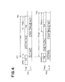
- FIG. 4 is a diagram for explaining transfer-in timings according to a second embodiment of the present invention.
- FIG. 4 for example, when a wafer W is transferred into the load lock chamber LL1 at a time TP1, periods PSS1 and PSS2 for the process chambers PM1 and PM2 to get ready to permit a transfer of the next wafer W thereinto are calculated based on this time TP1 respectively.
- TR(11m) in FIG. 4 represents an exchanging period in the load lock chamber LL1 or LL2.
- a wafer W to be transferred to the process ship PS1 can be selected from the load ports LP1 to LP3, so that selection can be made in a manner to give a priority to one having a shorter recipe period.
- the periods PSS can be calculated as follows in accordance with the numbers of wafers W transferred in the process ships PS1 and PS2.
- the calculation of the period PSS is performed based on the timing for exchange of wafers W between the process chamber PM1 or PM2 and the load lock chamber LL1 or LL2. Therefore, it is only required to calculate a waiting period PMb for transfer-in during which the wafer W transferred into the load lock chamber LL1 or LL2 is kept waiting until it is transferred into the process chamber PM1 or PM2, and add this waiting period PMb for transfer-in to the period PSL.
- the waiting period PMb for transfer-in during which the wafer W transferred into the load lock chamber LL1 or LL2 is kept waiting until it is transferred into the process chamber PM1 or PM2 is 0, and therefore the equations here are the same as the equation (1), (2), and (5).
- the period PSS can be obtained by adding PMb to the equations (3) and (4) respectively.
- the recalculation when there is a wafer W on the orienter OR can be performed by the calculation method similar to that of the equation (6) except that PMo is used in place of PMa in the equations (7) and (8). Note that PMo represents the process processing period for the wafer W on the orienter OR.
- the transfer chamber TR which is kept open to atmospheric air has been described as an example, but vacuum drawing of the transfer chamber TR may be performed.
- the loader arms LA1 and LA2 have been described with a case in which they are accessible to the wafer mounting tables B11 and B21 on the front side, but they may be configured to directly access the wafer mounting tables B12 and B22 on the back side.
- the loader arms LA1 and LA2 in a two-tire structure have been described, but a one-tier loader arm is also applicable.
- a cluster tool and a transfer control method according to the present invention are usable in the semiconductor manufacturing industry in which semiconductor devices are manufactured, and so on. Therefore, they have industrial applicability.
Landscapes
- Container, Conveyance, Adherence, Positioning, Of Wafer (AREA)
Abstract
Description
In the case where PSL > TR(LM): PMx = PMs
TR(in) = PSL at destination
In the case where PSL < TR(LM): PMx = PMs - TR(LM)
(however, it is 0 when PMs < TR(LM))
TR(in) = TR(LM) Note that PMx represents the processing residual period in the process chamber PM1 or PM2 in consideration of processing in the load lock chamber LL1 or LL2, and therefore when obtaining PSL at the destination, ΔPM in the equations (3) to (5) is replaced with PMx. Besides, TR(LM) represents the transfer period from one of the load ports LP1 to LP3 to the load lock chamber LL1 or LL2, and can be expressed, for example, by the period of transfer from the remotest load port LP3 via the orienter OR to the load lock chamber LL1 or LL2. PMs represents the processing residual period in the process chamber PM1 or PM2 after the wafer W is exchanged with another and transferred to the process chamber PM1 or PM2 and the load lock chamber LL1 or LL2 is opened to atmospheric air, and can be obtained as follows:
In the case where PMt > VENT: PMs = PMt - VENT
In the case where PMt < VENT: PMs = 0Note that PMt represents the processing period in the process chamber PM1 or PM2 for the wafer W before processed in the load lock chamber LL1 or LL2.
In the case where PSL > TR(LM): TR(in) = PSL at destination
In the case where PSL < TR(LM): TR(in) = TR(LM)
In the case where PMc > TR(in): PMx = PMc - TR(in)
In the case where TR(in) < PMc: PMx = 0 Note that PMc represents the processing residual period in the process chamber PM1 or PM2 for the wafer W in the process chamber PM1 or PM2.It should be noted that when there is no wafer W in the process chamber PM1 or PM2, calculation is conducted with the processing residual period ΔPM in the process chamber PM1 or PM2 as 0.
In the case where PSL > TR(LM): TR(in) = PSL at destination
In the case where PSL < TR(LM): TR(in) = TR(LM)
Tllm = VAC + TR(llm) + VENT.
Here,
PMa: process period for the wafer W transferred into the load lock chamber LL1 or LL2
Tllm: processing period in the load lock chamber LL1 or LL2.
Claims (12)
- A cluster tool, comprising:a plurality of process chambers for performing process processing for objects to be processed;load lock chambers coupled to said process chambers respectively for transferring the objects to be processed to said process chambers;a loader module coupled to said load lock chambers for transferring the objects to be processed to said load lock chambers; anda transfer control unit for selecting an object to be processed that is to be transferred next by said loader module, based on timings for when said load lock chambers get ready to permit transfers of the objects to be processed thereto.
- The cluster tool as set forth in claim 1, wherein said transfer control unit comprises:a transfer period calculating unit for calculating a period for each of said load lock chambers to get ready to permit a next transfer thereto, when the object to be processed is transferred into any one of said load lock chambers; anda selecting unit for selecting, as an object to be processed that is to be transferred next, an object to be processed having the shortest period to get ready to be transferable.
- The cluster tool as set forth in claim 2, wherein said loader module is provided with a positioning mechanism for positioning the object to be processed.
- The cluster tool as set forth in claim 4, wherein the object to be processed that is to be transferred next selected by said transfer control unit is positioned by said positioning mechanism, thereafter transferred to the front of said load lock chamber, and kept waiting.
- A cluster tool, comprising:a plurality of process chambers for performing process processing for objects to be processed;load lock chambers coupled to said process chambers respectively for transferring the objects to be processed to said process chambers;a loader module coupled to said load lock chambers for transferring the objects to be processed to said load lock chambers; anda transfer control unit for selecting an object to be processed that is to be transferred next by said loader module, based on timings for when said load lock chambers get ready to permit transfers of the objects to be processed thereto.
- The cluster tool as set forth in claim 5, wherein said transfer control unit comprises:a transfer period calculating unit for calculating a period for each of said load lock chambers to get ready to permit a next transfer thereto, when the object to be processed is transferred into any one of said load lock chambers; anda selecting unit for selecting, as an object to be processed that is to be transferred next, an object to be processed having the shortest period to get ready to be transferable.
- The cluster tool as set forth in claim 6, wherein said loader module is provided with a positioning mechanism for positioning the object to be processed.
- The cluster tool as set forth in claim 7, wherein the object to be processed that is to be transferred next selected by said transfer control unit is positioned by said positioning mechanism, thereafter transferred to the front of said load lock chamber, and kept waiting.
- A transfer control method of transferring objects to be processed via load lock chambers to a plurality of process chambers provided, comprising:selecting an object to be processed that is to be transferred next based on timings for when the load lock chambers get ready to permit transfers of the objects to be processed thereto.
- The transfer control method as set forth in claim 9, further comprising:positioning the selected object to be processed that is to be transferred next by a positioning mechanism, thereafter transferring the object to the front of the load lock chamber, and keeping the object waiting.
- A transfer control method of transferring objects to be processed via load lock chambers to a plurality of process chambers provided, comprising:selecting an object to be processed that is to be transferred next based on timings for when the load lock chambers get ready to permit transfers of the objects to be processed thereto.
- The transfer control method as set forth in claim 11, further comprising:positioning the selected object to be processed that is to be transferred next by a positioning mechanism, thereafter transferring the object to the front of the load lock chamber, and keeping the object waiting.
Applications Claiming Priority (3)
| Application Number | Priority Date | Filing Date | Title |
|---|---|---|---|
| JP2001108926 | 2001-04-06 | ||
| JP2001108926A JP4937459B2 (en) | 2001-04-06 | 2001-04-06 | Cluster tool and transfer control method |
| PCT/JP2002/003283 WO2002084731A1 (en) | 2001-04-06 | 2002-04-02 | Cluster tool and method for controlling transport |
Publications (3)
| Publication Number | Publication Date |
|---|---|
| EP1394849A1 true EP1394849A1 (en) | 2004-03-03 |
| EP1394849A4 EP1394849A4 (en) | 2009-06-24 |
| EP1394849B1 EP1394849B1 (en) | 2012-01-25 |
Family
ID=18960976
Family Applications (1)
| Application Number | Title | Priority Date | Filing Date |
|---|---|---|---|
| EP02707288A Expired - Lifetime EP1394849B1 (en) | 2001-04-06 | 2002-04-02 | Cluster tool and method for controlling transport |
Country Status (7)
| Country | Link |
|---|---|
| US (2) | US6970770B2 (en) |
| EP (1) | EP1394849B1 (en) |
| JP (1) | JP4937459B2 (en) |
| KR (1) | KR100571878B1 (en) |
| CN (1) | CN1320624C (en) |
| TW (1) | TW550638B (en) |
| WO (1) | WO2002084731A1 (en) |
Cited By (1)
| Publication number | Priority date | Publication date | Assignee | Title |
|---|---|---|---|---|
| EP3217421A1 (en) * | 2014-06-24 | 2017-09-13 | EV Group E. Thallner GmbH | Device for surface treating substrates |
Families Citing this family (31)
| Publication number | Priority date | Publication date | Assignee | Title |
|---|---|---|---|---|
| JPH0936198A (en) * | 1995-07-19 | 1997-02-07 | Hitachi Ltd | Vacuum processing apparatus and semiconductor manufacturing line using the same |
| TW442891B (en) * | 1998-11-17 | 2001-06-23 | Tokyo Electron Ltd | Vacuum processing system |
| JP4937459B2 (en) * | 2001-04-06 | 2012-05-23 | 東京エレクトロン株式会社 | Cluster tool and transfer control method |
| JP3674864B2 (en) * | 2003-03-25 | 2005-07-27 | 忠素 玉井 | Vacuum processing equipment |
| JP2004349503A (en) * | 2003-05-22 | 2004-12-09 | Tokyo Electron Ltd | Processing system and processing method for object to be processed |
| US7226512B2 (en) * | 2003-06-18 | 2007-06-05 | Ekc Technology, Inc. | Load lock system for supercritical fluid cleaning |
| JP2005322762A (en) * | 2004-05-10 | 2005-11-17 | Hitachi Kokusai Electric Inc | Substrate processing equipment |
| TWI278416B (en) * | 2004-12-09 | 2007-04-11 | Au Optronics Corp | Cassette stocker |
| KR100621775B1 (en) * | 2005-04-15 | 2006-09-15 | 삼성전자주식회사 | Substrate Cleaning Equipment |
| CN100511629C (en) * | 2005-10-06 | 2009-07-08 | 东京毅力科创株式会社 | Processing system and operating method thereof |
| JP2008075135A (en) * | 2006-09-21 | 2008-04-03 | Nippon Dempa Kogyo Co Ltd | Vacuum processing apparatus and air release method |
| CN101584034B (en) * | 2007-06-19 | 2011-05-18 | 株式会社爱发科 | Substrate carrying method |
| US8430620B1 (en) | 2008-03-24 | 2013-04-30 | Novellus Systems, Inc. | Dedicated hot and cold end effectors for improved throughput |
| JP2010062534A (en) * | 2008-06-30 | 2010-03-18 | Intevac Inc | System and method for substrate transport |
| WO2010014761A1 (en) | 2008-07-29 | 2010-02-04 | Intevac, Inc. | Processing tool with combined sputter and evaporation deposition sources |
| US20100162955A1 (en) * | 2008-12-31 | 2010-07-01 | Lawrence Chung-Lai Lei | Systems and methods for substrate processing |
| US20100162954A1 (en) * | 2008-12-31 | 2010-07-01 | Lawrence Chung-Lai Lei | Integrated facility and process chamber for substrate processing |
| US7897525B2 (en) * | 2008-12-31 | 2011-03-01 | Archers Inc. | Methods and systems of transferring, docking and processing substrates |
| US8110511B2 (en) * | 2009-01-03 | 2012-02-07 | Archers Inc. | Methods and systems of transferring a substrate to minimize heat loss |
| US8367565B2 (en) * | 2008-12-31 | 2013-02-05 | Archers Inc. | Methods and systems of transferring, docking and processing substrates |
| WO2013077322A1 (en) * | 2011-11-23 | 2013-05-30 | 日本電産サンキョー株式会社 | Work transfer system |
| SG2014013015A (en) * | 2012-05-30 | 2014-08-28 | Ev Group E Thallner Gmbh | Device and method for bonding of substrates |
| US9558974B2 (en) * | 2012-09-27 | 2017-01-31 | Taiwan Semiconductor Manufacturing Company, Ltd. | Semiconductor processing station and method for processing semiconductor wafer |
| JP6377717B2 (en) * | 2013-03-15 | 2018-08-22 | アプライド マテリアルズ インコーポレイテッドApplied Materials,Incorporated | Temperature control system and method for small lot substrate handling system |
| US9245783B2 (en) | 2013-05-24 | 2016-01-26 | Novellus Systems, Inc. | Vacuum robot with linear translation carriage |
| JP2014236193A (en) * | 2013-06-05 | 2014-12-15 | Sppテクノロジーズ株式会社 | Substrate transfer apparatus, and substrate transfer method using the same |
| JP6121846B2 (en) * | 2013-08-15 | 2017-04-26 | 株式会社Screenホールディングス | Substrate processing apparatus, substrate processing method, and substrate processing system |
| CN103529652B (en) * | 2013-10-23 | 2015-04-15 | 深圳市华星光电技术有限公司 | Sheet inlet and outlet controlling method and device for cooling and buffering mechanism for precise length measuring machine |
| CN105336652B (en) * | 2014-06-26 | 2019-05-31 | 北京北方华创微电子装备有限公司 | Chip transmission control method and system |
| JP7324811B2 (en) * | 2021-09-22 | 2023-08-10 | 株式会社Kokusai Electric | SUBSTRATE PROCESSING APPARATUS, SEMICONDUCTOR DEVICE MANUFACTURING METHOD, AND PROGRAM |
| JP7578120B2 (en) * | 2022-06-23 | 2024-11-06 | 日新イオン機器株式会社 | Substrate transport method and substrate processing apparatus |
Family Cites Families (21)
| Publication number | Priority date | Publication date | Assignee | Title |
|---|---|---|---|---|
| US5019233A (en) * | 1988-10-31 | 1991-05-28 | Eaton Corporation | Sputtering system |
| US5685684A (en) * | 1990-11-26 | 1997-11-11 | Hitachi, Ltd. | Vacuum processing system |
| JPH05275511A (en) * | 1991-03-01 | 1993-10-22 | Tokyo Electron Ltd | Transfer system and processing device for object to be processed |
| JP2751975B2 (en) * | 1991-12-20 | 1998-05-18 | 株式会社日立製作所 | Load lock chamber of semiconductor processing equipment |
| JPH05218176A (en) * | 1992-02-07 | 1993-08-27 | Tokyo Electron Tohoku Kk | Heat treatment and transfer of article to be treated |
| JPH0786369A (en) * | 1993-09-10 | 1995-03-31 | Matsushita Electric Ind Co Ltd | Combined processing equipment with multiple processing means |
| JPH0919853A (en) * | 1995-07-03 | 1997-01-21 | Seiko Epson Corp | Production management device and production management method using the device |
| JPH0936198A (en) * | 1995-07-19 | 1997-02-07 | Hitachi Ltd | Vacuum processing apparatus and semiconductor manufacturing line using the same |
| US6481956B1 (en) * | 1995-10-27 | 2002-11-19 | Brooks Automation Inc. | Method of transferring substrates with two different substrate holding end effectors |
| US6091498A (en) * | 1996-07-15 | 2000-07-18 | Semitool, Inc. | Semiconductor processing apparatus having lift and tilt mechanism |
| US6431807B1 (en) * | 1998-07-10 | 2002-08-13 | Novellus Systems, Inc. | Wafer processing architecture including single-wafer load lock with cooling unit |
| JP2000174091A (en) * | 1998-12-01 | 2000-06-23 | Fujitsu Ltd | Transfer device and manufacturing device |
| JP4256551B2 (en) * | 1998-12-25 | 2009-04-22 | 東京エレクトロン株式会社 | Vacuum processing system |
| JP3748193B2 (en) * | 1999-03-17 | 2006-02-22 | 株式会社日立製作所 | Vacuum processing apparatus and operation method thereof |
| US6244811B1 (en) * | 1999-06-29 | 2001-06-12 | Lam Research Corporation | Atmospheric wafer transfer module with nest for wafer transport robot |
| JP2000100720A (en) * | 1999-07-14 | 2000-04-07 | Nikon Corp | Lithography system, exposure apparatus, semiconductor device manufacturing method using the same, and machine controller |
| AU6763000A (en) * | 1999-08-11 | 2001-03-05 | Multilevel Metals, Inc. | Load lock system for foups |
| US6248262B1 (en) * | 2000-02-03 | 2001-06-19 | General Electric Company | Carbon-reinforced thermoplastic resin composition and articles made from same |
| JP2001358195A (en) | 2000-06-15 | 2001-12-26 | Mitsubishi Electric Corp | Semiconductor manufacturing method and apparatus |
| JP4937459B2 (en) * | 2001-04-06 | 2012-05-23 | 東京エレクトロン株式会社 | Cluster tool and transfer control method |
| US6719517B2 (en) * | 2001-12-04 | 2004-04-13 | Brooks Automation | Substrate processing apparatus with independently configurable integral load locks |
-
2001
- 2001-04-06 JP JP2001108926A patent/JP4937459B2/en not_active Expired - Fee Related
-
2002
- 2002-04-02 EP EP02707288A patent/EP1394849B1/en not_active Expired - Lifetime
- 2002-04-02 CN CNB028074955A patent/CN1320624C/en not_active Expired - Fee Related
- 2002-04-02 WO PCT/JP2002/003283 patent/WO2002084731A1/en not_active Ceased
- 2002-04-02 KR KR1020037013032A patent/KR100571878B1/en not_active Expired - Fee Related
- 2002-04-02 US US10/473,135 patent/US6970770B2/en not_active Expired - Lifetime
- 2002-04-04 TW TW091106834A patent/TW550638B/en not_active IP Right Cessation
-
2005
- 2005-05-16 US US11/129,327 patent/US7245987B2/en not_active Expired - Fee Related
Cited By (1)
| Publication number | Priority date | Publication date | Assignee | Title |
|---|---|---|---|---|
| EP3217421A1 (en) * | 2014-06-24 | 2017-09-13 | EV Group E. Thallner GmbH | Device for surface treating substrates |
Also Published As
| Publication number | Publication date |
|---|---|
| US7245987B2 (en) | 2007-07-17 |
| EP1394849B1 (en) | 2012-01-25 |
| EP1394849A4 (en) | 2009-06-24 |
| WO2002084731A1 (en) | 2002-10-24 |
| US20050220577A1 (en) | 2005-10-06 |
| KR20030090713A (en) | 2003-11-28 |
| US6970770B2 (en) | 2005-11-29 |
| JP4937459B2 (en) | 2012-05-23 |
| KR100571878B1 (en) | 2006-04-18 |
| JP2002305225A (en) | 2002-10-18 |
| CN1547768A (en) | 2004-11-17 |
| CN1320624C (en) | 2007-06-06 |
| US20040117059A1 (en) | 2004-06-17 |
| TW550638B (en) | 2003-09-01 |
Similar Documents
| Publication | Publication Date | Title |
|---|---|---|
| EP1394849B1 (en) | Cluster tool and method for controlling transport | |
| JP5543318B2 (en) | Substrate transfer method | |
| US7630785B2 (en) | Substrate processing system for setting uniform module cycle length and access control time lag in two pipeline processing systems | |
| US20090259335A1 (en) | Substrate Processing System | |
| US8467895B2 (en) | Processing system and method for operating the same | |
| JP4334817B2 (en) | Substrate processing apparatus and substrate processing method | |
| JP2005322762A (en) | Substrate processing equipment | |
| JP4477982B2 (en) | Cluster tool processing system and dwell time monitoring program | |
| US6684123B2 (en) | Method and apparatus for accessing a multiple chamber semiconductor wafer processing system | |
| KR20040024156A (en) | Single type vacuum chamber system for processing semiconductor wafer | |
| JP2005252105A (en) | Substrate processing equipment | |
| CN121023458A (en) | A wafer deposition equipment and its scheduling method | |
| KR20060064943A (en) | Semiconductor manufacturing apparatus and process progress method using the same | |
| JP2009024229A (en) | Substrate processing equipment |
Legal Events
| Date | Code | Title | Description |
|---|---|---|---|
| PUAI | Public reference made under article 153(3) epc to a published international application that has entered the european phase |
Free format text: ORIGINAL CODE: 0009012 |
|
| 17P | Request for examination filed |
Effective date: 20031104 |
|
| AK | Designated contracting states |
Kind code of ref document: A1 Designated state(s): AT BE CH CY DE DK ES FI FR GB GR IE IT LI LU MC NL PT SE TR |
|
| AX | Request for extension of the european patent |
Extension state: AL LT LV MK RO SI |
|
| A4 | Supplementary search report drawn up and despatched |
Effective date: 20090527 |
|
| RIC1 | Information provided on ipc code assigned before grant |
Ipc: H01L 21/00 20060101AFI20090519BHEP |
|
| 17Q | First examination report despatched |
Effective date: 20091123 |
|
| GRAP | Despatch of communication of intention to grant a patent |
Free format text: ORIGINAL CODE: EPIDOSNIGR1 |
|
| RBV | Designated contracting states (corrected) |
Designated state(s): DE |
|
| GRAS | Grant fee paid |
Free format text: ORIGINAL CODE: EPIDOSNIGR3 |
|
| GRAA | (expected) grant |
Free format text: ORIGINAL CODE: 0009210 |
|
| AK | Designated contracting states |
Kind code of ref document: B1 Designated state(s): DE |
|
| RAP1 | Party data changed (applicant data changed or rights of an application transferred) |
Owner name: TOKYO ELECTRON LIMITED |
|
| REG | Reference to a national code |
Ref country code: DE Ref legal event code: R096 Ref document number: 60242069 Country of ref document: DE Effective date: 20120329 |
|
| PLBE | No opposition filed within time limit |
Free format text: ORIGINAL CODE: 0009261 |
|
| STAA | Information on the status of an ep patent application or granted ep patent |
Free format text: STATUS: NO OPPOSITION FILED WITHIN TIME LIMIT |
|
| 26N | No opposition filed |
Effective date: 20121026 |
|
| REG | Reference to a national code |
Ref country code: DE Ref legal event code: R097 Ref document number: 60242069 Country of ref document: DE Effective date: 20121026 |
|
| PGFP | Annual fee paid to national office [announced via postgrant information from national office to epo] |
Ref country code: DE Payment date: 20170329 Year of fee payment: 16 |
|
| REG | Reference to a national code |
Ref country code: DE Ref legal event code: R119 Ref document number: 60242069 Country of ref document: DE |
|
| PG25 | Lapsed in a contracting state [announced via postgrant information from national office to epo] |
Ref country code: DE Free format text: LAPSE BECAUSE OF NON-PAYMENT OF DUE FEES Effective date: 20181101 |