EP1394554A1 - Process for the fabrication of a threshold acceleration sensor - Google Patents
Process for the fabrication of a threshold acceleration sensor Download PDFInfo
- Publication number
- EP1394554A1 EP1394554A1 EP02425539A EP02425539A EP1394554A1 EP 1394554 A1 EP1394554 A1 EP 1394554A1 EP 02425539 A EP02425539 A EP 02425539A EP 02425539 A EP02425539 A EP 02425539A EP 1394554 A1 EP1394554 A1 EP 1394554A1
- Authority
- EP
- European Patent Office
- Prior art keywords
- sample element
- process according
- forming
- layer
- substrate
- Prior art date
- Legal status (The legal status is an assumption and is not a legal conclusion. Google has not performed a legal analysis and makes no representation as to the accuracy of the status listed.)
- Granted
Links
- 238000000034 method Methods 0.000 title claims abstract description 42
- 230000008569 process Effects 0.000 title claims abstract description 39
- 238000004519 manufacturing process Methods 0.000 title claims abstract description 19
- 230000001133 acceleration Effects 0.000 title description 7
- 239000000758 substrate Substances 0.000 claims abstract description 29
- 238000005530 etching Methods 0.000 claims abstract description 12
- 239000004065 semiconductor Substances 0.000 claims abstract description 11
- 238000004873 anchoring Methods 0.000 claims description 24
- VYPSYNLAJGMNEJ-UHFFFAOYSA-N Silicium dioxide Chemical compound O=[Si]=O VYPSYNLAJGMNEJ-UHFFFAOYSA-N 0.000 claims description 12
- 229910021420 polycrystalline silicon Inorganic materials 0.000 claims description 12
- 229920005591 polysilicon Polymers 0.000 claims description 11
- 239000000463 material Substances 0.000 claims description 10
- 235000012239 silicon dioxide Nutrition 0.000 claims description 6
- 239000000377 silicon dioxide Substances 0.000 claims description 6
- 238000007493 shaping process Methods 0.000 claims description 2
- 239000011248 coating agent Substances 0.000 claims 1
- 238000000576 coating method Methods 0.000 claims 1
- 239000004020 conductor Substances 0.000 claims 1
- 239000003989 dielectric material Substances 0.000 claims 1
- 238000012360 testing method Methods 0.000 description 6
- 238000005538 encapsulation Methods 0.000 description 4
- 238000001020 plasma etching Methods 0.000 description 3
- 230000000284 resting effect Effects 0.000 description 3
- 230000008901 benefit Effects 0.000 description 2
- 239000002131 composite material Substances 0.000 description 2
- 239000002019 doping agent Substances 0.000 description 2
- 238000005259 measurement Methods 0.000 description 2
- 238000005459 micromachining Methods 0.000 description 2
- 230000010355 oscillation Effects 0.000 description 2
- 238000012545 processing Methods 0.000 description 2
- XUIMIQQOPSSXEZ-UHFFFAOYSA-N Silicon Chemical compound [Si] XUIMIQQOPSSXEZ-UHFFFAOYSA-N 0.000 description 1
- 230000009471 action Effects 0.000 description 1
- 150000001875 compounds Chemical class 0.000 description 1
- 230000006835 compression Effects 0.000 description 1
- 238000007906 compression Methods 0.000 description 1
- 230000008878 coupling Effects 0.000 description 1
- 238000010168 coupling process Methods 0.000 description 1
- 238000005859 coupling reaction Methods 0.000 description 1
- 230000007547 defect Effects 0.000 description 1
- 230000008021 deposition Effects 0.000 description 1
- 238000013461 design Methods 0.000 description 1
- 230000000873 masking effect Effects 0.000 description 1
- 238000004377 microelectronic Methods 0.000 description 1
- 238000012986 modification Methods 0.000 description 1
- 230000004048 modification Effects 0.000 description 1
- 229910021421 monocrystalline silicon Inorganic materials 0.000 description 1
- 230000003647 oxidation Effects 0.000 description 1
- 238000007254 oxidation reaction Methods 0.000 description 1
- 230000001681 protective effect Effects 0.000 description 1
- 230000035945 sensitivity Effects 0.000 description 1
- 230000035939 shock Effects 0.000 description 1
- 229910052710 silicon Inorganic materials 0.000 description 1
- 239000010703 silicon Substances 0.000 description 1
- 238000005476 soldering Methods 0.000 description 1
- 238000013519 translation Methods 0.000 description 1
Images




Classifications
-
- H—ELECTRICITY
- H01—ELECTRIC ELEMENTS
- H01H—ELECTRIC SWITCHES; RELAYS; SELECTORS; EMERGENCY PROTECTIVE DEVICES
- H01H1/00—Contacts
- H01H1/0036—Switches making use of microelectromechanical systems [MEMS]
-
- G—PHYSICS
- G01—MEASURING; TESTING
- G01P—MEASURING LINEAR OR ANGULAR SPEED, ACCELERATION, DECELERATION, OR SHOCK; INDICATING PRESENCE, ABSENCE, OR DIRECTION, OF MOVEMENT
- G01P1/00—Details of instruments
- G01P1/02—Housings
- G01P1/023—Housings for acceleration measuring devices
-
- G—PHYSICS
- G01—MEASURING; TESTING
- G01P—MEASURING LINEAR OR ANGULAR SPEED, ACCELERATION, DECELERATION, OR SHOCK; INDICATING PRESENCE, ABSENCE, OR DIRECTION, OF MOVEMENT
- G01P15/00—Measuring acceleration; Measuring deceleration; Measuring shock, i.e. sudden change of acceleration
- G01P15/02—Measuring acceleration; Measuring deceleration; Measuring shock, i.e. sudden change of acceleration by making use of inertia forces using solid seismic masses
- G01P15/04—Measuring acceleration; Measuring deceleration; Measuring shock, i.e. sudden change of acceleration by making use of inertia forces using solid seismic masses for indicating maximum value
- G01P15/06—Measuring acceleration; Measuring deceleration; Measuring shock, i.e. sudden change of acceleration by making use of inertia forces using solid seismic masses for indicating maximum value using members subjected to a permanent deformation
-
- G—PHYSICS
- G01—MEASURING; TESTING
- G01P—MEASURING LINEAR OR ANGULAR SPEED, ACCELERATION, DECELERATION, OR SHOCK; INDICATING PRESENCE, ABSENCE, OR DIRECTION, OF MOVEMENT
- G01P15/00—Measuring acceleration; Measuring deceleration; Measuring shock, i.e. sudden change of acceleration
- G01P15/02—Measuring acceleration; Measuring deceleration; Measuring shock, i.e. sudden change of acceleration by making use of inertia forces using solid seismic masses
- G01P15/08—Measuring acceleration; Measuring deceleration; Measuring shock, i.e. sudden change of acceleration by making use of inertia forces using solid seismic masses with conversion into electric or magnetic values
- G01P15/0802—Details
-
- G—PHYSICS
- G01—MEASURING; TESTING
- G01P—MEASURING LINEAR OR ANGULAR SPEED, ACCELERATION, DECELERATION, OR SHOCK; INDICATING PRESENCE, ABSENCE, OR DIRECTION, OF MOVEMENT
- G01P15/00—Measuring acceleration; Measuring deceleration; Measuring shock, i.e. sudden change of acceleration
- G01P15/02—Measuring acceleration; Measuring deceleration; Measuring shock, i.e. sudden change of acceleration by making use of inertia forces using solid seismic masses
- G01P15/08—Measuring acceleration; Measuring deceleration; Measuring shock, i.e. sudden change of acceleration by making use of inertia forces using solid seismic masses with conversion into electric or magnetic values
- G01P15/0891—Measuring acceleration; Measuring deceleration; Measuring shock, i.e. sudden change of acceleration by making use of inertia forces using solid seismic masses with conversion into electric or magnetic values with indication of predetermined acceleration values
-
- G—PHYSICS
- G01—MEASURING; TESTING
- G01P—MEASURING LINEAR OR ANGULAR SPEED, ACCELERATION, DECELERATION, OR SHOCK; INDICATING PRESENCE, ABSENCE, OR DIRECTION, OF MOVEMENT
- G01P15/00—Measuring acceleration; Measuring deceleration; Measuring shock, i.e. sudden change of acceleration
- G01P15/18—Measuring acceleration; Measuring deceleration; Measuring shock, i.e. sudden change of acceleration in two or more dimensions
-
- G—PHYSICS
- G01—MEASURING; TESTING
- G01P—MEASURING LINEAR OR ANGULAR SPEED, ACCELERATION, DECELERATION, OR SHOCK; INDICATING PRESENCE, ABSENCE, OR DIRECTION, OF MOVEMENT
- G01P15/00—Measuring acceleration; Measuring deceleration; Measuring shock, i.e. sudden change of acceleration
- G01P15/02—Measuring acceleration; Measuring deceleration; Measuring shock, i.e. sudden change of acceleration by making use of inertia forces using solid seismic masses
- G01P15/08—Measuring acceleration; Measuring deceleration; Measuring shock, i.e. sudden change of acceleration by making use of inertia forces using solid seismic masses with conversion into electric or magnetic values
- G01P2015/0805—Measuring acceleration; Measuring deceleration; Measuring shock, i.e. sudden change of acceleration by making use of inertia forces using solid seismic masses with conversion into electric or magnetic values being provided with a particular type of spring-mass-system for defining the displacement of a seismic mass due to an external acceleration
- G01P2015/0808—Measuring acceleration; Measuring deceleration; Measuring shock, i.e. sudden change of acceleration by making use of inertia forces using solid seismic masses with conversion into electric or magnetic values being provided with a particular type of spring-mass-system for defining the displacement of a seismic mass due to an external acceleration for defining in-plane movement of the mass, i.e. movement of the mass in the plane of the substrate
- G01P2015/0811—Measuring acceleration; Measuring deceleration; Measuring shock, i.e. sudden change of acceleration by making use of inertia forces using solid seismic masses with conversion into electric or magnetic values being provided with a particular type of spring-mass-system for defining the displacement of a seismic mass due to an external acceleration for defining in-plane movement of the mass, i.e. movement of the mass in the plane of the substrate for one single degree of freedom of movement of the mass
- G01P2015/0814—Measuring acceleration; Measuring deceleration; Measuring shock, i.e. sudden change of acceleration by making use of inertia forces using solid seismic masses with conversion into electric or magnetic values being provided with a particular type of spring-mass-system for defining the displacement of a seismic mass due to an external acceleration for defining in-plane movement of the mass, i.e. movement of the mass in the plane of the substrate for one single degree of freedom of movement of the mass for translational movement of the mass, e.g. shuttle type
-
- H—ELECTRICITY
- H01—ELECTRIC ELEMENTS
- H01H—ELECTRIC SWITCHES; RELAYS; SELECTORS; EMERGENCY PROTECTIVE DEVICES
- H01H35/00—Switches operated by change of a physical condition
- H01H35/14—Switches operated by change of acceleration, e.g. by shock or vibration, inertia switch
- H01H35/146—Switches operated by change of acceleration, e.g. by shock or vibration, inertia switch operated by plastic deformation or rupture of structurally associated elements
Definitions
- the present invention relates to a process for the fabrication of an inertial sensor with failure threshold.
- MEMS sensors are sensors that can be integrated in a semiconductor chip and are suitable for detecting various quantities.
- MEMS accelerometers with capacitive unbalancing are known.
- these accelerometers are normally provided with a fixed body and of a mobile mass, both of which are conductive and are capacitively coupled together.
- the capacitance present between the fixed body and the mobile mass may vary, and its value depends upon the relative position of the mobile mass with respect to the fixed body.
- the accelerometer is subjected to a stress, the mobile mass is displaced with respect to the fixed body and causes a variation in the coupling capacitance, which is detected by a special sensing circuit.
- MEMS accelerometers are extremely sensitive and precise; however, they are not suitable for being used in many applications, mainly because they are complex to make and their cost is very high.
- the processes of fabrication involve the execution of numerous non-standard steps and/or the use of non-standard substrates (for example, SOI substrates); on the other hand, it is normally necessary to provide feedback sensing circuits based upon differential charge amplifiers, the design of which frequently involves some difficulties.
- the purpose of the present invention is to provide a process for the fabrication of an inertial sensor with failure threshold, which will enable the problems described above to be overcome.
- a wafer 1 of semiconductor material for example monocrystalline silicon, comprises a substrate 2, on which a thin pad oxide layer 3, for example 2.5 ⁇ m thick, is thermally grown.
- a conductive layer 5 of polysilicon having for example a thickness of between 400 and 800 nm and a dopant concentration of 10 19 atoms/cm 3 , is then deposited on the pad oxide layer 3 and is defined by means of a photolithographic process.
- Two T-shaped samples 6 are thus obtained, having respective feet 6a, aligned with respect to one another and extending towards one another, and respective arms 6b parallel to one another ( Figures 2-4).
- each sample 6 is set in directions identified by a first axis X and, respectively, by a second axis Y, which are mutually orthogonal (a third axis Z, orthogonal to the first axis X and the second axis Y, is illustrated in Figure 2).
- anchoring pads 8 are made, of a substantially rectangular shape and having a width greater than the arms 6b.
- each of the samples 6 has a first weakened region 9 and a second weakened region 10.
- the first weakened region 9 and the second weakened region 10 are made as narrowed portions of the foot 6a and, respectively, of one of the arms 6b.
- the weakened regions 9, 10 are defined by notches 11 with a circular or polygonal profile, made in an area of joining 6c between the foot 6a and the arms 6b and traversing the sample 6 in a direction parallel to the third axis Z.
- the thickness of the conductive layer 5 of polysilicon, the dimensions of the feet 6a and of the arms 6b of the samples 6, and the conformation of the weakened regions 9, 10 determine the mechanical resistance to failure of the samples .6 themselves.
- a sacrificial layer 12 of silicon dioxide is deposited so as to coat the pad oxide layer 3 and the samples 6.
- the pad oxide layer 3 and the sacrificial layer 12 form a single sacrificial region in which the samples 6 are embedded.
- the sacrificial layer 12 is then defined by means of a photolithographic process comprising two masking steps. During a first step, first openings 14 are made in the sacrificial layer 12, exposing respective ends of the feet 6b of the samples 6, as illustrated in Figure 5. In a second step of the photolithographic process ( Figure 6), both the sacrificial layer 12 and the pad oxide layer 3 are selectively etched, so as to make second openings 15, exposing portions of the substrate 2.
- a conductive epitaxial layer 16 is grown on the wafer 1, the said layer having a thickness, for example, of 15 ⁇ m and a dopant concentration of 10 18 atoms/cm 3 .
- the epitaxial layer 16 coats the sacrificial layer 12 entirely and extends in depth through the first and the second openings 14, 15 until the samples 6 and the substrate 2, respectively, are reached ( Figure 7 and 8).
- the epitaxial layer 16 is then selectively etched, preferably by reactive-ion etching (RIE), and the sacrificial layer 12 and the pad oxide layer 3 are removed.
- RIE reactive-ion etching
- the following are formed: a mobile mass 18; anchorages 19, provided on the portions of the substrate 2 previously exposed by the second openings 15; a plurality of springs 20, connecting the mobile mass 18 to the anchorages 19; and a ring-shaped supporting structure 21, which surrounds the mobile mass 18, the samples 6, the springs 20, and the corresponding anchorages 19 (see Figure 9, in which the sacrificial layer 12 and the pad oxide layer 3 have already been removed) .
- the mobile mass 18 is connected to the substrate 2 by the springs 20, which are in turn constrained to the anchorages 19 ( Figure 11).
- the springs 20, which are per se known, are shaped so as to enable oscillations of the mobile mass 18 with respect to the substrate 2 along each of the three axes X, Y, Z, at the same time, however, preventing rotations.
- the mobile mass 18 is moreover constrained to the substrate 2 through the samples 6.
- the mobile mass 18 has, in a median portion, a pair of anchoring blocks 22, projecting outwards in opposite directions along the second axis Y.
- the anchoring blocks 22 are connected to the end of the foot 6a of a respective one of the samples 6, as illustrated in Figure 10.
- the samples 6 are anchored to the substrate 2 through the anchoring pads 8.
- the silicon dioxide is in fact removed only partially underneath the anchoring pads 8, which are wider than the feet 6a and the arms 6b of the samples 6; thus, residual portions 3' of the pad oxide layer 3, which are not etched, fix the anchoring pads 8 to the substrate 2, serving as bonding elements.
- the mobile mass 18 is suspended at a distance on the substrate 2 and can oscillate about a resting position, in accordance with the degrees of freedom allowed by the springs 20 (in particular, it can translate along the axes X, Y and Z).
- the samples 6. are elastic elements, which connect the mobile mass 18 to the substrate 2 in a way similar to the springs 20.
- the samples are shaped so as to be subjected to a stress when the mobile mass 18 is outside a relative resting position with respect to the substrate 2.
- the samples 6 are, however, very thin and have preferential failure points in areas corresponding to the weakened regions 9, 10. For this reason, their mechanical resistance to failure is much lower than that of the springs 20, and they undergo failure in a controlled way when they are subjected to a stress of pre-set intensity.
- the mobile mass 18, the substrate 2, the springs 20 with the anchorages 19, and the samples 6 form an inertial sensor 24, the operation of which will be described in detail hereinafter.
- An encapsulation structure 25 for the inertial sensor 24 is then applied on top of the wafer 1, forming a composite wafer 26 ( Figure 12).
- the encapsulation structure 25 is an additional semiconductor wafer, in which a recess 27 has previously been opened, in a region that is to be laid on top of the mobile mass 18.
- the encapsulation structure 25 is coupled to the ring-shaped supporting structure 21 by the interposition of a layer of soldering 29.
- the compound wafer 26 is cut into a plurality of dice 30, each die comprising an inertial sensor 24 and a respective protective cap 31, formed by the fractioning of the encapsulation structure 25 ( Figure 13).
- the die 30 is finally mounted on a device 32, for example a cellphone.
- the device 32 is provided with a casing 33, inside which the die 30 is fixed, as illustrated in Figure 14.
- the inertial sensor 24 is connected to terminals of a testing circuit 35, which measures the value of electrical resistance between said terminals.
- the anchoring pads 8 of the arms 6b, in which the second weakened regions 10 are formed are connected each to a respective terminal of the testing circuit 35.
- the samples 6 and the mobile mass 18 form a conductive path that enables passage of current between any given pair of anchoring pads 8.
- the testing circuit 35 detects low values of electrical resistance between the anchoring pads 8.
- the device 32 undergoes modest stresses, which cause slight oscillations of the mobile mass 18 about the resting position, without jeopardizing the integrity of the inertial sensor 24.
- the mobile mass 18 of the inertial sensor 24 undergoes a sharp acceleration and subjects the samples 6 and the springs 20 to a force. According to the intensity of the stress transmitted to the inertial sensor 24, said force can exceed one of the thresholds of mechanical failure of the samples 6, which consequently break. In particular, failure occurs at one of the weakened regions 9, 10, which have minimum strength. In either case, the conductive path between the two anchoring pads 8 connected to the testing circuit 35 is interrupted, and hence the testing circuit detects a high value of electrical resistance between its own terminals, thus enabling recognition of the occurrence of events that are liable to damage the device 32.
- T-shaped samples 37 are provided, which present a single weakened region 38.
- the weakened region 38 is a narrowed portion defined by a pair of notches 39, which are oblique with respect to a foot 37a and arms 37b of the samples 37.
- the two T-shaped samples 6 are located in a gap 36 between the substrate 2 and the mobile mass 18 and have the end of the respective feet 6a in mutual contact.
- both of the samples 6 are fixed to a single anchoring block 22' set centrally with respect to the mobile mass 18 itself.
- the process according to the invention has the following advantages.
- processing steps that are standard in the microelectronics industry are employed.
- the following steps are carried out: steps of deposition of both insulating and conductive layers of material; photolithographic processes; a step of epitaxial growth; and standard steps of etching of the epitaxial silicon and of the insulating layers.
- a single step of thermal oxidation is carried out, and consequently the wafer 1 is subjected to modest stresses during the fabrication process. The yield of the process is therefore high.
- the inertial sensor 24 is obtained starting from a standard, lowcost substrate.
- inertial sensors with failure threshold are particularly suitable for use where it is necessary to record the occurrence of stresses that are harmful for a device in which they are incorporated and in which it is superfluous to provide precise measurements of accelerations. For example, they can be advantageously used for verifying the validity of the warranty in the case of widely used electronic devices, such as, for example, cellphones.
- the inertial sensors provided with the present method have contained overall dimensions.
- large dimensions are generally due to the mobile mass, which must ensure the necessary precision and sensitivity.
- inertial sensors obtained using the process described are more advantageous because they respond in a substantially isotropic way to the mechanical stress. In practice, therefore, just one inertial sensor is sufficient to detect forces acting in any direction.
- FIG. 19 A second embodiment of the invention is illustrated in Figures 19 and 20, where parts that are the same as the ones already illustrated are designated by the same reference numbers.
- an inertial sensor 40 is made, having L-shaped samples 41.
- the samples 41 are obtained by shaping a conductive polysilicon layer deposited on top of a pad oxide layer (not illustrated herein), which has in turn been grown on the substrate 42 of a semiconductor wafer 43.
- the mobile mass 18, the anchorages 19 and the springs 20 are subsequently obtained.
- the samples 41 have first ends connected to respective anchoring blocks 22 of the mobile mass 18, and second ends terminating with respective anchoring pads 41 fixed to the substrate 2, as explained previously.
- notches 42 made at respective vertices 43 of the samples 41 define weakened regions 44 of the samples 40.
- Figures 21 and 22 illustrate a third embodiment of the invention, according to which an inertial sensor 50 is obtained, made on a substrate 54 and provided with substantially rectilinear samples 51 that extend parallel to the first axis X.
- an inertial sensor 50 is obtained, made on a substrate 54 and provided with substantially rectilinear samples 51 that extend parallel to the first axis X.
- two anchorages 52 and two springs 53 of a known type are provided, which connect the mobile mass 18 to the anchorages 52 and are shaped so as to prevent substantially the rotation of the mobile mass 18 itself about the first axis X.
- the samples 51 have first ends soldered to respective anchoring blocks 22 of the mobile mass 18 and second ends terminating with anchoring pads 55, made as described previously.
- pairs of transverse opposed notches 57 define respective weakened regions 58 along the samples 51 ( Figure 22).
- the weakened regions may be absent.
- the inertial sensor 50 responds preferentially to stresses oriented according to a plane orthogonal to the samples 51, i.e., the plane defined by the second axis Y and by the third axis Z.
- a plane orthogonal to the samples 51 i.e., the plane defined by the second axis Y and by the third axis Z.
- to detect stresses in a substantially isotropic way it is possible to use two sensors 50 connected in series between the terminals of a testing circuit 59 and rotated through 90° with respect to one another, as illustrated in Figure 23.
- a pad oxide layer 62 is grown on a semiconductor wafer 60 having a substrate 61.
- a conductive layer 63 of polycrystalline silicon (here indicated by a dashed line) is deposited on the pad oxide layer 61 and is defined to form a sample 64, which is substantially rectilinear and extends parallel to the first axis X ( Figure 25).
- the sample 64 has an anchoring pad 65 at one of its ends and has a weakened region 66 defined by a pair of notches 67 in a central position.
- a sacrificial layer 69 of silicon dioxide is deposited so as to coat the entire wafer 60 and is then selectively removed to form an opening 68 at one end of the sample 64 opposite to the anchoring pad 65.
- An epitaxial layer 70 is then grown ( Figure 26), which is etched so as to form a mobile mass 71, anchorages 72, springs 73, and a supporting ring (not illustrated for reasons of convenience).
- the sacrificial layer 69 and the pad oxide layer 62 are removed, except for a residual portion 62' of the pad oxide layer 62 underlying the anchoring pad 65 ( Figures 27 and 28).
- the mobile mass 71 and the sample 64 are thus freed. More precisely, the mobile mass 71, which has, at its centre, a through opening 74 on top of the sample 64, is constrained to the substrate 61 through the anchorages 72 and the springs 73, which are shaped so as to prevent any translation along or rotation about the first axis X.
- the sample 65 has opposite ends, one connected to the substrate 2 through the anchoring pad 65, and the other to the mobile mass 71, and is placed in a gap 76 comprised between the mobile mass 71 and the substrate 61.
- the use of a single anchoring point between the sample and the mobile mass advantageously enables effective relaxation of the stresses due to expansion of the mobile mass.
- the sample is T-shaped, like the ones illustrated in Figure 9.
- Figure 29 illustrates a detail of a sample 81, for example a rectilinear one, of an inertial sensor obtained using a fifth embodiment of the process according to the invention.
- the sample 81 has a weakened region defined by a transverse groove 82 extending between opposite sides 83 of the sample 81.
- the groove 82 is obtained by means of masked etching of controlled duration of the sample 81 ( Figure 30).
- a first layer 85 of polysilicon is deposited and defined. Then, a stop layer 86 of silicon dioxide and a second layer 87 of polysilicon are formed. Finally, a groove 82' is dug by etching the second layer 87 of polysilicon as far as the stop layer 86.
- the weakened regions can be defined by using side notches in the samples together with grooves extending between the side notches.
- the weakened regions could be defined by through openings that traverse the samples, instead of by side notches.
Landscapes
- Physics & Mathematics (AREA)
- General Physics & Mathematics (AREA)
- Electromagnetism (AREA)
- Pressure Sensors (AREA)
- Micromachines (AREA)
Abstract
Description
- The present invention relates to a process for the fabrication of an inertial sensor with failure threshold.
- As is known, modern techniques of micromachining of semiconductors can be advantageously exploited for making various extremely sensitive and precise sensors, having further small overall dimensions. The so-called MEMS sensors (or micro-electro-mechanical-system sensors), are sensors that can be integrated in a semiconductor chip and are suitable for detecting various quantities. In particular, both linear and rotational MEMS accelerometers with capacitive unbalancing are known. In brief, these accelerometers are normally provided with a fixed body and of a mobile mass, both of which are conductive and are capacitively coupled together. In addition, the capacitance present between the fixed body and the mobile mass may vary, and its value depends upon the relative position of the mobile mass with respect to the fixed body. When the accelerometer is subjected to a stress, the mobile mass is displaced with respect to the fixed body and causes a variation in the coupling capacitance, which is detected by a special sensing circuit.
- As mentioned previously, MEMS accelerometers are extremely sensitive and precise; however, they are not suitable for being used in many applications, mainly because they are complex to make and their cost is very high. On the one hand, in fact, the processes of fabrication involve the execution of numerous non-standard steps and/or the use of non-standard substrates (for example, SOI substrates); on the other hand, it is normally necessary to provide feedback sensing circuits based upon differential charge amplifiers, the design of which frequently involves some difficulties.
- In addition, in many cases the precision of capacitive MEMS sensors is not required and, indeed, it is not even necessary to have an instantaneous measurement of the value of acceleration. On the contrary, it is frequently just necessary to verify whether a device incorporating the accelerometer has undergone accelerations higher than a pre-set threshold, normally on account of impact. For example, the majority of electronic devices commonly used, such as cellphones, are protected by a warranty, which, however, is no longer valid if any malfunctioning is due not to defects of fabrication but to an impact consequent on the device being dropped or in any case on a use that is not in conformance with the instructions. Unless visible damage is found, such as marks on the casing or breaking of some parts, it is practically impossible to demonstrate that the device has suffered damage that invalidates the warranty. On the other hand, portable devices, such as cellphones, exactly, are particularly exposed to being dropped and consequently to getting broken, precisely on account of how they are used.
- Events of the above type could be easily detected by an inertial sensor, which is able to record accelerations higher than a pre-set threshold. However, the use of MEMS accelerometers of a capacitive type in these cases would evidently lead to excessive costs. It would thus be desirable to have available sensors that can be made using techniques of micromachining of semiconductors, consequently having overall dimensions comparable to those of capacitive MEMS sensors, but simpler as regards both the structure of the sensor and the sensing circuit. In addition, also the processes of fabrication should be, as a whole, simple and inexpensive.
- The purpose of the present invention is to provide a process for the fabrication of an inertial sensor with failure threshold, which will enable the problems described above to be overcome.
- According to the present invention, a process is provided for the fabrication of an inertial sensor with failure threshold, as defined in
Claim 1. - For a better understanding of the invention, some embodiments thereof are now described, purely by way of non-limiting examples and with reference to the attached drawings, in which:
- Figures 1 and 2 are cross-sectional views through a semiconductor wafer in successive steps of fabrication in a first embodiment of the process according to the present invention;
- Figure 3 is a top plan view of the wafer of Figure 2;
- Figure 4 illustrates an enlarged detail of Figure 3;
- Figure 5 is a cross-sectional view of the wafer of Figure 3 in a subsequent fabrication step;
- Figure 6 is a top plan view of the wafer of Figure 5;
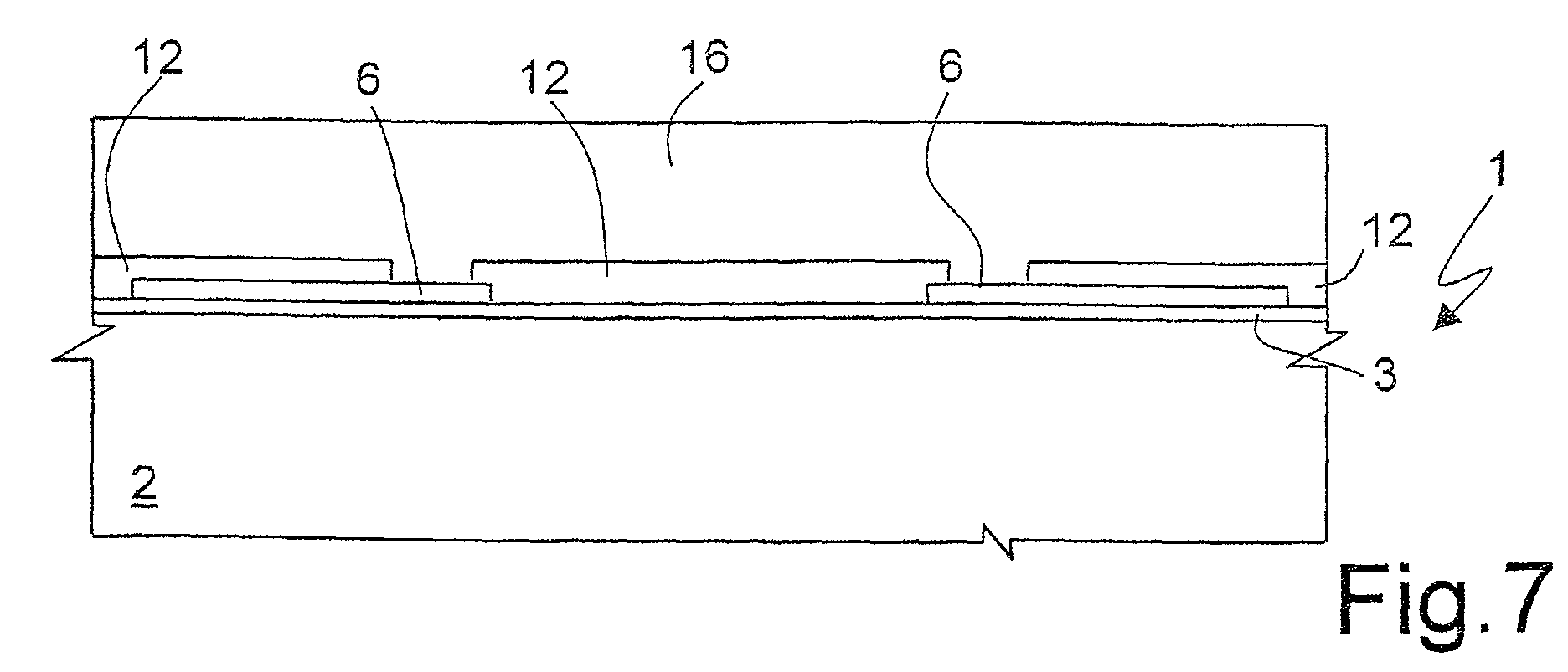
- Figures 7 and 8 are cross-sectional views of the wafer of Figure 6 in a subsequent fabrication step, taken along the planes of trace VII-VII and VIII-VIII, respectively, of Figure 6;
- Figure 9 is a top plan view of the wafer of Figure 7, in a subsequent fabrication step, in which an inertial sensor is obtained;
- Figures 10 and 11 are cross-sectional views of the wafer of Figure 9, taken along the planes of trace X-X and XI-XI, respectively, of Figure 9;
- Figures 12 and 13 are cross-sectional views through a composite wafer and a die, respectively, obtained starting from the wafer of Figure 9;
- Figure 14 is a schematic view of the top three quarters of a device incorporating the die of Figure 13;
- Figure 15 is a schematic illustration of an inertial sensor of the type illustrated in Figures 9-13 in an operative configuration;
- Figure 16 is a detail of an inertial sensor obtained according to a variant of the first embodiment of the present process;
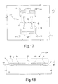
- Figure 17 is a top plan view of an inertial sensor obtained according to a further variant of the first embodiment of the present process;
- Figure 18 is a cross-sectional view of the sensor of Figure 17;
- Figure 19 is a top plan view of an inertial sensor obtained according to a second embodiment of the present invention;
- Figure 20 illustrates an enlarged detail of Figure 19;
- Figure 21 is a top plan view of an inertial sensor obtained according to a third embodiment of the present invention;
- Figure 22 illustrates an enlarged detail of Figure 21;
- Figure 23 is a schematic illustration of two inertial sensors of the type illustrated in Figure 21 in an operative configuration;
- Figure 24 is a cross-sectional view through a semiconductor wafer in an initial fabrication step of a process according to a fourth embodiment of the present invention;
- Figure 25 is a top plan view of the wafer of Figure 24;
- Figure 26 illustrates the wafer of Figure 24 in a subsequent fabrication step;
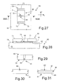
- Figure 27 is a top plan view of the wafer of Figure 26 in a subsequent fabrication step, in which an inertial sensor is obtained;
- Figure 28 is a cross-sectional view through the wafer of Figure 27, taken according to the plane of trace XXVI-XXVI of Figure 27;
- Figure 29 is a plan view of a detail of an inertial sensor obtained according to a fifth embodiment of the present invention
- Figure 30 is a side view of the detail of Figure 29; and
- Figure 31 is a side view of the detail of Figure 29, obtained according to a variant of the fifth embodiment of the present invention.
- With reference to Figures 1-13, a
wafer 1 of semiconductor material, for example monocrystalline silicon, comprises asubstrate 2, on which a thinpad oxide layer 3, for example 2.5 µm thick, is thermally grown. Aconductive layer 5 of polysilicon, having for example a thickness of between 400 and 800 nm and a dopant concentration of 1019 atoms/cm3, is then deposited on thepad oxide layer 3 and is defined by means of a photolithographic process. Two T-shaped samples 6 are thus obtained, havingrespective feet 6a, aligned with respect to one another and extending towards one another, andrespective arms 6b parallel to one another (Figures 2-4). Thefeet 6a and thearms 6b of eachsample 6 are set in directions identified by a first axis X and, respectively, by a second axis Y, which are mutually orthogonal (a third axis Z, orthogonal to the first axis X and the second axis Y, is illustrated in Figure 2). In addition, at respective ends of thearms 6b of both thesamples 6anchoring pads 8 are made, of a substantially rectangular shape and having a width greater than thearms 6b. As illustrated in Figure 4, each of thesamples 6 has a first weakenedregion 9 and a second weakenedregion 10. In particular, in both of thesamples 6, the first weakenedregion 9 and the second weakenedregion 10 are made as narrowed portions of thefoot 6a and, respectively, of one of thearms 6b. In addition, the weakenedregions notches 11 with a circular or polygonal profile, made in an area of joining 6c between thefoot 6a and thearms 6b and traversing thesample 6 in a direction parallel to the third axis Z. The thickness of theconductive layer 5 of polysilicon, the dimensions of thefeet 6a and of thearms 6b of thesamples 6, and the conformation of the weakenedregions notches 11 defining the first weakenedregion 9 and the second weakenedregion 10, it is possible to obtain pre-set failure thresholds of thesamples 6 along the first, second and third axes X, Y and Z. Preferably, all the mechanical failure thresholds are basically the same. - Next, a
sacrificial layer 12 of silicon dioxide is deposited so as to coat thepad oxide layer 3 and thesamples 6. In practice, thepad oxide layer 3 and thesacrificial layer 12 form a single sacrificial region in which thesamples 6 are embedded. Thesacrificial layer 12 is then defined by means of a photolithographic process comprising two masking steps. During a first step,first openings 14 are made in thesacrificial layer 12, exposing respective ends of thefeet 6b of thesamples 6, as illustrated in Figure 5. In a second step of the photolithographic process (Figure 6), both thesacrificial layer 12 and thepad oxide layer 3 are selectively etched, so as to makesecond openings 15, exposing portions of thesubstrate 2. - Subsequently, a conductive
epitaxial layer 16 is grown on thewafer 1, the said layer having a thickness, for example, of 15 µm and a dopant concentration of 1018 atoms/cm3. In detail, theepitaxial layer 16 coats thesacrificial layer 12 entirely and extends in depth through the first and thesecond openings samples 6 and thesubstrate 2, respectively, are reached (Figure 7 and 8). - The
epitaxial layer 16 is then selectively etched, preferably by reactive-ion etching (RIE), and thesacrificial layer 12 and thepad oxide layer 3 are removed. In greater detail, during the step of etching of theepitaxial layer 16, the following are formed: amobile mass 18;anchorages 19, provided on the portions of thesubstrate 2 previously exposed by thesecond openings 15; a plurality ofsprings 20, connecting themobile mass 18 to theanchorages 19; and a ring-shaped supportingstructure 21, which surrounds themobile mass 18, thesamples 6, thesprings 20, and the corresponding anchorages 19 (see Figure 9, in which thesacrificial layer 12 and thepad oxide layer 3 have already been removed) . - The
mobile mass 18 is connected to thesubstrate 2 by thesprings 20, which are in turn constrained to the anchorages 19 (Figure 11). Thesprings 20, which are per se known, are shaped so as to enable oscillations of themobile mass 18 with respect to thesubstrate 2 along each of the three axes X, Y, Z, at the same time, however, preventing rotations. Themobile mass 18 is moreover constrained to thesubstrate 2 through thesamples 6. In greater detail, themobile mass 18 has, in a median portion, a pair of anchoring blocks 22, projecting outwards in opposite directions along the second axis Y. The anchoring blocks 22 are connected to the end of thefoot 6a of a respective one of thesamples 6, as illustrated in Figure 10. In turn, thesamples 6 are anchored to thesubstrate 2 through theanchoring pads 8. By controlling the duration of etching of thesacrificial layer 12 and of thepad oxide layer 3, the silicon dioxide is in fact removed only partially underneath theanchoring pads 8, which are wider than thefeet 6a and thearms 6b of thesamples 6; thus, residual portions 3' of thepad oxide layer 3, which are not etched, fix theanchoring pads 8 to thesubstrate 2, serving as bonding elements. - The
sacrificial layer 12 and the remaining portions of thepad oxide layer 3 are, instead, completely removed and, hence, themobile mass 18 and thesamples 6 are freed. In practice, themobile mass 18 is suspended at a distance on thesubstrate 2 and can oscillate about a resting position, in accordance with the degrees of freedom allowed by the springs 20 (in particular, it can translate along the axes X, Y and Z). Also thesamples 6. are elastic elements, which connect themobile mass 18 to thesubstrate 2 in a way similar to thesprings 20. In particular, the samples are shaped so as to be subjected to a stress when themobile mass 18 is outside a relative resting position with respect to thesubstrate 2. Thesamples 6 are, however, very thin and have preferential failure points in areas corresponding to the weakenedregions springs 20, and they undergo failure in a controlled way when they are subjected to a stress of pre-set intensity. - In practice, at this stage of the process, the
mobile mass 18, thesubstrate 2, thesprings 20 with theanchorages 19, and thesamples 6 form aninertial sensor 24, the operation of which will be described in detail hereinafter. - An encapsulation structure 25 for the
inertial sensor 24 is then applied on top of thewafer 1, forming a composite wafer 26 (Figure 12). In particular, the encapsulation structure 25 is an additional semiconductor wafer, in which arecess 27 has previously been opened, in a region that is to be laid on top of themobile mass 18. The encapsulation structure 25 is coupled to the ring-shaped supportingstructure 21 by the interposition of a layer ofsoldering 29. Next, thecompound wafer 26 is cut into a plurality ofdice 30, each die comprising aninertial sensor 24 and a respectiveprotective cap 31, formed by the fractioning of the encapsulation structure 25 (Figure 13). - The
die 30 is finally mounted on adevice 32, for example a cellphone. Preferably, thedevice 32 is provided with acasing 33, inside which thedie 30 is fixed, as illustrated in Figure 14. In addition (Figure 15), theinertial sensor 24 is connected to terminals of atesting circuit 35, which measures the value of electrical resistance between said terminals. In greater in detail, theanchoring pads 8 of thearms 6b, in which the second weakenedregions 10 are formed, are connected each to a respective terminal of thetesting circuit 35. - In normal conditions, i.e., when the
inertial sensor 24 is intact, thesamples 6 and themobile mass 18 form a conductive path that enables passage of current between any given pair ofanchoring pads 8. In practice, thetesting circuit 35 detects low values of electrical resistance between theanchoring pads 8. During normal use, thedevice 32 undergoes modest stresses, which cause slight oscillations of themobile mass 18 about the resting position, without jeopardizing the integrity of theinertial sensor 24. - When the
device 32 suffers a shock, themobile mass 18 of theinertial sensor 24 undergoes a sharp acceleration and subjects thesamples 6 and thesprings 20 to a force. According to the intensity of the stress transmitted to theinertial sensor 24, said force can exceed one of the thresholds of mechanical failure of thesamples 6, which consequently break. In particular, failure occurs at one of the weakenedregions anchoring pads 8 connected to thetesting circuit 35 is interrupted, and hence the testing circuit detects a high value of electrical resistance between its own terminals, thus enabling recognition of the occurrence of events that are liable to damage thedevice 32. - According to a variant of the embodiment described, shown in Figure 16, T-shaped
samples 37 are provided, which present a single weakenedregion 38. In particular, the weakenedregion 38 is a narrowed portion defined by a pair ofnotches 39, which are oblique with respect to afoot 37a andarms 37b of thesamples 37. - According to a further variant, illustrated in Figures 17 and 18, the two T-shaped
samples 6 are located in agap 36 between thesubstrate 2 and themobile mass 18 and have the end of therespective feet 6a in mutual contact. In addition, both of thesamples 6 are fixed to a single anchoring block 22' set centrally with respect to themobile mass 18 itself. - The process according to the invention has the following advantages. In the first place, for fabrication of the
inertial sensor 24, processing steps that are standard in the microelectronics industry are employed. In particular, the following steps are carried out: steps of deposition of both insulating and conductive layers of material; photolithographic processes; a step of epitaxial growth; and standard steps of etching of the epitaxial silicon and of the insulating layers. Advantageously, a single step of thermal oxidation is carried out, and consequently thewafer 1 is subjected to modest stresses during the fabrication process. The yield of the process is therefore high. In addition, theinertial sensor 24 is obtained starting from a standard, lowcost substrate. - The process described consequently enables inertial sensors with failure threshold to be produced at a very low cost. Such sensors are particularly suitable for use where it is necessary to record the occurrence of stresses that are harmful for a device in which they are incorporated and in which it is superfluous to provide precise measurements of accelerations. For example, they can be advantageously used for verifying the validity of the warranty in the case of widely used electronic devices, such as, for example, cellphones.
- In addition, the inertial sensors provided with the present method have contained overall dimensions. In inertial sensors, in fact, large dimensions are generally due to the mobile mass, which must ensure the necessary precision and sensitivity. In this case, instead, it is sufficient that, in the event of a predetermined acceleration, the mobile mass will cause breaking of the weakened regions of the samples, which have low strength. It is consequently evident that also the mobile mass can have contained overall dimensions.
- The use of a single anchoring point between the samples and the mobile mass, as illustrated in the second variant of Figures 17 and 18, has a further advantage as compared to the ones already pointed out, because it enables more effective relaxation of the stresses due to expansion of the materials. In particular, it may happen that the polysilicon parts which are even only partially embedded in the silicon dioxide (samples and portions of the epitaxial layer) will be subjected to a compressive force, since both the polysilicon, and the oxide tend to a expand in opposite directions during the fabrication process. When the oxide is removed, the action of compression on the polysilicon is eliminated, and the polysilicon can thus expand. Clearly, the largest expansion, in absolute terms, is that of the mobile mass, since it has the largest size. The use of a single anchoring point, instead of two anchorages set at a distance apart enables more effective relaxation of the stresses due to said expansion, since the mobile mass can expand freely, without modifying the load state of the samples.
- The inertial sensors obtained using the process described are more advantageous because they respond in a substantially isotropic way to the mechanical stress. In practice, therefore, just one inertial sensor is sufficient to detect forces acting in any direction.
- A second embodiment of the invention is illustrated in Figures 19 and 20, where parts that are the same as the ones already illustrated are designated by the same reference numbers. According to said embodiment, an
inertial sensor 40 is made, having L-shapedsamples 41. As in the previous case, thesamples 41 are obtained by shaping a conductive polysilicon layer deposited on top of a pad oxide layer (not illustrated herein), which has in turn been grown on thesubstrate 42 of asemiconductor wafer 43. Using processing steps similar to the ones already described, themobile mass 18, theanchorages 19 and thesprings 20 are subsequently obtained. - In detail, the
samples 41 have first ends connected to respective anchoring blocks 22 of themobile mass 18, and second ends terminating withrespective anchoring pads 41 fixed to thesubstrate 2, as explained previously. In addition,notches 42 made atrespective vertices 43 of thesamples 41 define weakenedregions 44 of thesamples 40. - Figures 21 and 22 illustrate a third embodiment of the invention, according to which an
inertial sensor 50 is obtained, made on asubstrate 54 and provided with substantiallyrectilinear samples 51 that extend parallel to the first axis X. In this case, during the RIE etching step, in addition to themobile mass 18, twoanchorages 52 and twosprings 53 of a known type are provided, which connect themobile mass 18 to theanchorages 52 and are shaped so as to prevent substantially the rotation of themobile mass 18 itself about the first axis X. - The
samples 51 have first ends soldered to respective anchoring blocks 22 of themobile mass 18 and second ends terminating with anchoringpads 55, made as described previously. In addition, pairs of transverseopposed notches 57 define respective weakenedregions 58 along the samples 51 (Figure 22). - Alternatively, the weakened regions may be absent.
- The
inertial sensor 50 responds preferentially to stresses oriented according to a plane orthogonal to thesamples 51, i.e., the plane defined by the second axis Y and by the third axis Z. In this case, to detect stresses in a substantially isotropic way, it is possible to use twosensors 50 connected in series between the terminals of atesting circuit 59 and rotated through 90° with respect to one another, as illustrated in Figure 23. - With reference to Figures 24-28, according to a fourth embodiment of the invention, a
pad oxide layer 62 is grown on asemiconductor wafer 60 having asubstrate 61. Next, aconductive layer 63 of polycrystalline silicon (here indicated by a dashed line) is deposited on thepad oxide layer 61 and is defined to form asample 64, which is substantially rectilinear and extends parallel to the first axis X (Figure 25). Thesample 64 has ananchoring pad 65 at one of its ends and has a weakenedregion 66 defined by a pair ofnotches 67 in a central position. - A
sacrificial layer 69 of silicon dioxide is deposited so as to coat theentire wafer 60 and is then selectively removed to form an opening 68 at one end of thesample 64 opposite to theanchoring pad 65. - An
epitaxial layer 70 is then grown (Figure 26), which is etched so as to form amobile mass 71,anchorages 72, springs 73, and a supporting ring (not illustrated for reasons of convenience). Thesacrificial layer 69 and thepad oxide layer 62 are removed, except for a residual portion 62' of thepad oxide layer 62 underlying the anchoring pad 65 (Figures 27 and 28). Themobile mass 71 and thesample 64 are thus freed. More precisely, themobile mass 71, which has, at its centre, a through opening 74 on top of thesample 64, is constrained to thesubstrate 61 through theanchorages 72 and thesprings 73, which are shaped so as to prevent any translation along or rotation about the first axis X. In addition, thesample 65 has opposite ends, one connected to thesubstrate 2 through theanchoring pad 65, and the other to themobile mass 71, and is placed in agap 76 comprised between themobile mass 71 and thesubstrate 61. - In this way, an
inertial sensor 80 is obtained, which is then encapsulated through steps similar to the ones described with reference to Figures 12 and 13. - Also in this case, the use of a single anchoring point between the sample and the mobile mass advantageously enables effective relaxation of the stresses due to expansion of the mobile mass.
- According to one variant (not illustrated), the sample is T-shaped, like the ones illustrated in Figure 9.
- Figure 29 illustrates a detail of a
sample 81, for example a rectilinear one, of an inertial sensor obtained using a fifth embodiment of the process according to the invention. In particular, thesample 81 has a weakened region defined by atransverse groove 82 extending betweenopposite sides 83 of thesample 81. - The
groove 82 is obtained by means of masked etching of controlled duration of the sample 81 (Figure 30). - Alternatively (Figure 31), a
first layer 85 of polysilicon is deposited and defined. Then, astop layer 86 of silicon dioxide and asecond layer 87 of polysilicon are formed. Finally, a groove 82' is dug by etching thesecond layer 87 of polysilicon as far as thestop layer 86. - Finally, it is evident that modifications and variations may be made to the process described herein, without thereby departing from the scope of the present invention. In particular, the weakened regions can be defined by using side notches in the samples together with grooves extending between the side notches. In addition, the weakened regions could be defined by through openings that traverse the samples, instead of by side notches.
Claims (15)
- A process for the fabrication of an inertial sensor with failure threshold, comprising the steps of:forming, on top of a substrate (2; 42; 61) of a semiconductor wafer (1; 43; 60), at least one sample element (6; 40; 51; 64; 81; 81') embedded in a sacrificial region (3, 12; 62, 69);forming, on top of said sacrificial region (3, 12; 62, 69), a body (18; 71) connected to said sample element (6; 40; 51; 64; 81; 81'); andetching said sacrificial region (3, 12; 62, 69), so as to free said body (18; 71) and said sample element (6; 40; 51; 64; 81; 81').
- The process according to Claim 1, in which the step of forming said sample element (6; 40; 51; 64; 81; 81') comprises:forming a first layer (3; 62) of a first material, which coats said substrate (2; 61);forming a second layer (5; 63) of a second material, which coats said first layer (3; 62);shaping said second layer (5; 63), so as to define said sample element (6; 40; 51; 64; 81; 81'); andforming a third layer (12; 69) of said first material coating said first layer (3; 62) and said sample element (6; 40; 51; 64; 81; 81').
- The process according to Claim 2, in which said first material is a dielectric material and said second material is a conductive material.
- The process according to Claim 3, in which said first material is silicon dioxide and said second material is polysilicon.
- The process according to any one of the preceding claims, in which the step of forming at least one sample element (6; 40; 51; 64; 81; 81') comprises the step of making at least one weakened region (9, 10; 38; 42; 58; 66; 82; 82') of said sample element (6; 40; 51; 64; 81; 81').
- The process according to Claim 5, in which the step of making at least one weakened region (9, 10; 38; 42; 58; 66) comprises the step of defining a narrowing of said sample element (6; 40; 51; 64).
- The process according to Claim 6, in which said step of defining a narrowing portion comprises forming notches (11; 39; 42; 57; 67) in said sample element (6; 40; 51; 64)
- The process according to Claim 5, in which the step of making at least one weakened region (82; 82') comprises making a groove extending between opposite edges (83) of said sample element (81; 81').
- The process according to Claim 8, in which the step of making a groove comprises performing an etch of controlled duration of said sample element (81; 81').
- The process according to Claim 8, in which the step of making a groove comprises:forming a stop layer (86) inside said sample element (81'); andetching said sample element (81') until said stop element (86) is reached.
- The process according to any one of the preceding claims, in which the step of forming at least one sample element (6; 40; 51; 64; 81; 81') comprises defining at least one anchoring pad (8; 41; 55; 65) of said sample element (6; 40; 51; 64; 81; 81' ) .
- The process according to Claim 11, in which the step of etching said sacrificial region (3, 12; 62, 69) is interrupted before removing residual portions (3'; 62') of said sacrificial region (3, 12; 62, 69) underlying said anchoring pad (8; 41; 55; 65).
- The process according to any one of the preceding claims, in which before performing the step of forming said body (18; 71), through said sacrificial region (3, 12; 62, 69) there are made at least one first opening (14; 68), which exposes one end of said sample element (6), and second openings (15), which expose respective portions of said substrate (2).
- The process according to Claim 13, in which the step of forming said body (18; 71) comprises:growing an epitaxial layer (16; 70), which extends on top of said sacrificial region (3, 12; 62, 69) and through said first opening (14; 68) and said second openings (15); andetching said epitaxial layer (16; 70) until said sacrificial region is reached (3, 12; 62, 69).
- The process according to Claim 14, in which, during the step of etching said epitaxial layer (16; 70) there are defined anchorages (19; 52; 72) connected to said substrate (2; 42; 61) and elastic elements (20; 53; 73) connecting said body (18; 71) to said anchorages (19; 52; 72).
Priority Applications (4)
| Application Number | Priority Date | Filing Date | Title |
|---|---|---|---|
| EP02425539A EP1394554B1 (en) | 2002-08-30 | 2002-08-30 | Process for the fabrication of a threshold acceleration sensor |
| US10/650,275 US20040121504A1 (en) | 2002-08-30 | 2003-08-27 | Process for the fabrication of an inertial sensor with failure threshold |
| JP2003307928A JP4667731B2 (en) | 2002-08-30 | 2003-08-29 | Manufacturing process of inertial sensor with failure threshold |
| US11/566,590 US7678599B2 (en) | 2002-08-30 | 2006-12-04 | Process for the fabrication of an inertial sensor with failure threshold |
Applications Claiming Priority (1)
| Application Number | Priority Date | Filing Date | Title |
|---|---|---|---|
| EP02425539A EP1394554B1 (en) | 2002-08-30 | 2002-08-30 | Process for the fabrication of a threshold acceleration sensor |
Publications (2)
| Publication Number | Publication Date |
|---|---|
| EP1394554A1 true EP1394554A1 (en) | 2004-03-03 |
| EP1394554B1 EP1394554B1 (en) | 2011-11-02 |
Family
ID=31198026
Family Applications (1)
| Application Number | Title | Priority Date | Filing Date |
|---|---|---|---|
| EP02425539A Expired - Lifetime EP1394554B1 (en) | 2002-08-30 | 2002-08-30 | Process for the fabrication of a threshold acceleration sensor |
Country Status (3)
| Country | Link |
|---|---|
| US (2) | US20040121504A1 (en) |
| EP (1) | EP1394554B1 (en) |
| JP (1) | JP4667731B2 (en) |
Cited By (4)
| Publication number | Priority date | Publication date | Assignee | Title |
|---|---|---|---|---|
| EP2275384A1 (en) * | 2009-07-15 | 2011-01-19 | Nxp B.V. | Threshold acceleration sensor and method of manufacturing |
| WO2015080793A1 (en) * | 2013-11-26 | 2015-06-04 | Raytheon Company | High bandwidth linear flexure bearing |
| CN106076460A (en) * | 2016-06-15 | 2016-11-09 | 亚洲硅业(青海)有限公司 | A kind of device processing polycrystalline silicon rod and using method thereof |
| US10670825B2 (en) | 2018-08-23 | 2020-06-02 | Raytheon Company | Mounting devices with integrated alignment adjustment features and locking mechanisms |
Families Citing this family (6)
| Publication number | Priority date | Publication date | Assignee | Title |
|---|---|---|---|---|
| EP1394554B1 (en) * | 2002-08-30 | 2011-11-02 | STMicroelectronics Srl | Process for the fabrication of a threshold acceleration sensor |
| JP2007298408A (en) * | 2006-04-28 | 2007-11-15 | Matsushita Electric Works Ltd | Electrostatic capacity sensor |
| US8682606B2 (en) * | 2008-10-07 | 2014-03-25 | Qualcomm Incorporated | Generating virtual buttons using motion sensors |
| US8351910B2 (en) * | 2008-12-02 | 2013-01-08 | Qualcomm Incorporated | Method and apparatus for determining a user input from inertial sensors |
| US9297824B2 (en) * | 2012-09-14 | 2016-03-29 | Intel Corporation | Techniques, systems and devices related to acceleration measurement |
| TWI756860B (en) * | 2020-10-08 | 2022-03-01 | 緯創資通股份有限公司 | Channel structure for signal transmission |
Citations (2)
| Publication number | Priority date | Publication date | Assignee | Title |
|---|---|---|---|---|
| WO1998009174A1 (en) * | 1996-08-30 | 1998-03-05 | Fraunhofer-Gesellschaft zur Förderung der angewandten Forschung e.V. | Acceleration limit sensor |
| DE10005562A1 (en) * | 2000-02-09 | 2001-09-06 | Bosch Gmbh Robert | Leveling sensor for e.g. aligning laser device has acceleration measurement unit enclosed along with acceleration sensor via common frame |
Family Cites Families (24)
| Publication number | Priority date | Publication date | Assignee | Title |
|---|---|---|---|---|
| JPH05142243A (en) * | 1991-11-22 | 1993-06-08 | Omron Corp | Impact sensor and impact sensing device |
| JPH08138307A (en) * | 1994-09-16 | 1996-05-31 | Toshiba Corp | Information storage device |
| JPH10270719A (en) * | 1997-03-26 | 1998-10-09 | Mitsubishi Materials Corp | Semiconductor inertial sensor and method of manufacturing the same |
| JPH11250788A (en) * | 1998-02-27 | 1999-09-17 | Omron Corp | Physical quantity change recording element |
| US6794728B1 (en) * | 1999-02-24 | 2004-09-21 | Advanced Safety Concepts, Inc. | Capacitive sensors in vehicular environments |
| WO2001014842A1 (en) * | 1999-08-20 | 2001-03-01 | Hitachi, Ltd. | Semiconductor pressure sensor and pressure sensing device |
| US6508122B1 (en) * | 1999-09-16 | 2003-01-21 | American Gnc Corporation | Microelectromechanical system for measuring angular rate |
| JP2001108703A (en) * | 1999-10-08 | 2001-04-20 | Akebono Brake Ind Co Ltd | Impact detection display member |
| AU2002359370A1 (en) * | 2001-11-09 | 2003-05-26 | Coventor, Incorporated | Mems device having contact and standoff bumps and related methods |
| FI119078B (en) * | 2002-02-12 | 2008-07-15 | Nokia Corp | Accelerometer |
| US7064637B2 (en) * | 2002-07-18 | 2006-06-20 | Wispry, Inc. | Recessed electrode for electrostatically actuated structures |
| US7265429B2 (en) * | 2002-08-07 | 2007-09-04 | Chang-Feng Wan | System and method of fabricating micro cavities |
| US7429495B2 (en) * | 2002-08-07 | 2008-09-30 | Chang-Feng Wan | System and method of fabricating micro cavities |
| EP1394554B1 (en) * | 2002-08-30 | 2011-11-02 | STMicroelectronics Srl | Process for the fabrication of a threshold acceleration sensor |
| EP1394555B1 (en) * | 2002-08-30 | 2012-04-25 | STMicroelectronics S.r.l. | Threshold acceleration sensor |
| WO2005058133A2 (en) * | 2003-12-11 | 2005-06-30 | Proteus Biomedical, Inc. | Implantable pressure sensors |
| JP2006250769A (en) * | 2005-03-11 | 2006-09-21 | Seiko Epson Corp | Vibrating gyro element |
| US7528691B2 (en) * | 2005-08-26 | 2009-05-05 | Innovative Micro Technology | Dual substrate electrostatic MEMS switch with hermetic seal and method of manufacture |
| US7467552B2 (en) * | 2005-11-10 | 2008-12-23 | Honeywell International Inc. | Miniature package for translation of sensor sense axis |
| US7545622B2 (en) * | 2006-03-08 | 2009-06-09 | Wispry, Inc. | Micro-electro-mechanical system (MEMS) variable capacitors and actuation components and related methods |
| US7779688B2 (en) * | 2006-12-20 | 2010-08-24 | Epson Toyocom Corporation | Vibration gyro sensor |
| JP4915246B2 (en) * | 2007-01-26 | 2012-04-11 | セイコーエプソン株式会社 | Gyro module |
| JP4285548B2 (en) * | 2007-02-05 | 2009-06-24 | エプソントヨコム株式会社 | Gyro sensor module and angular velocity detection method |
| JP2009002735A (en) * | 2007-06-20 | 2009-01-08 | Epson Toyocom Corp | Angular velocity detector |
-
2002
- 2002-08-30 EP EP02425539A patent/EP1394554B1/en not_active Expired - Lifetime
-
2003
- 2003-08-27 US US10/650,275 patent/US20040121504A1/en not_active Abandoned
- 2003-08-29 JP JP2003307928A patent/JP4667731B2/en not_active Expired - Lifetime
-
2006
- 2006-12-04 US US11/566,590 patent/US7678599B2/en not_active Expired - Lifetime
Patent Citations (2)
| Publication number | Priority date | Publication date | Assignee | Title |
|---|---|---|---|---|
| WO1998009174A1 (en) * | 1996-08-30 | 1998-03-05 | Fraunhofer-Gesellschaft zur Förderung der angewandten Forschung e.V. | Acceleration limit sensor |
| DE10005562A1 (en) * | 2000-02-09 | 2001-09-06 | Bosch Gmbh Robert | Leveling sensor for e.g. aligning laser device has acceleration measurement unit enclosed along with acceleration sensor via common frame |
Cited By (7)
| Publication number | Priority date | Publication date | Assignee | Title |
|---|---|---|---|---|
| EP2275384A1 (en) * | 2009-07-15 | 2011-01-19 | Nxp B.V. | Threshold acceleration sensor and method of manufacturing |
| US9679857B2 (en) | 2009-07-15 | 2017-06-13 | Nxp B.V. | Semiconductor device and method including an intertial mass element |
| WO2015080793A1 (en) * | 2013-11-26 | 2015-06-04 | Raytheon Company | High bandwidth linear flexure bearing |
| US9222956B2 (en) | 2013-11-26 | 2015-12-29 | Raytheon Company | High bandwidth linear flexure bearing |
| CN106076460A (en) * | 2016-06-15 | 2016-11-09 | 亚洲硅业(青海)有限公司 | A kind of device processing polycrystalline silicon rod and using method thereof |
| CN106076460B (en) * | 2016-06-15 | 2018-04-13 | 亚洲硅业(青海)有限公司 | A kind of device and its application method for handling polycrystalline silicon rod |
| US10670825B2 (en) | 2018-08-23 | 2020-06-02 | Raytheon Company | Mounting devices with integrated alignment adjustment features and locking mechanisms |
Also Published As
| Publication number | Publication date |
|---|---|
| EP1394554B1 (en) | 2011-11-02 |
| US20040121504A1 (en) | 2004-06-24 |
| JP4667731B2 (en) | 2011-04-13 |
| US7678599B2 (en) | 2010-03-16 |
| US20070175865A1 (en) | 2007-08-02 |
| JP2004134763A (en) | 2004-04-30 |
Similar Documents
| Publication | Publication Date | Title |
|---|---|---|
| EP1394555B1 (en) | Threshold acceleration sensor | |
| EP0762510B1 (en) | Method for fabricating a monolithic semiconductor device with integrated surface micromachined structures | |
| US6146917A (en) | Fabrication method for encapsulated micromachined structures | |
| US8186221B2 (en) | Vertically integrated MEMS acceleration transducer | |
| US5417111A (en) | Monolithic chip containing integrated circuitry and suspended microstructure | |
| US5620931A (en) | Methods for fabricating monolithic device containing circuitry and suspended microstructure | |
| EP2871456A1 (en) | Pressure sensor | |
| TW201400401A (en) | Hybrid integrated component and method of manufacturing same | |
| US6500348B2 (en) | Deep reactive ion etching process and microelectromechanical devices formed thereby | |
| EP1394554B1 (en) | Process for the fabrication of a threshold acceleration sensor | |
| US6768628B2 (en) | Method for fabricating an isolated microelectromechanical system (MEMS) device incorporating a wafer level cap | |
| US6846724B2 (en) | Method for fabricating a microelectromechanical system (MEMS) device using a pre-patterned bridge | |
| US20160209344A1 (en) | Complex sensor and method of manufacturing the same | |
| CN110697647A (en) | MEMS sensor element and corresponding sensor, chip and method of manufacture | |
| US4873868A (en) | Force measurement sensor integrated on silicon, and a method of manufacture | |
| JPH03114272A (en) | Strain sensor and manufacture thereof | |
| KR100238999B1 (en) | Semiconductor micromachining method | |
| CN115014593B (en) | Pressure sensor and preparation method thereof | |
| JPH07273351A (en) | Semiconductor sensor | |
| JP2009079948A (en) | Semiconductor acceleration sensor and manufacturing method thereof | |
| WO2002091439A1 (en) | Fabrication of a microelectromechanical system (mems) device | |
| JP2006214963A (en) | Acceleration sensor, electronic device, and method of manufacturing acceleration sensor | |
| KR100298296B1 (en) | A ultra-small disposable threshold shock sensor and fabrication method thereof | |
| JP3405222B2 (en) | Semiconductor acceleration sensor element and method of manufacturing the same | |
| KR20050019758A (en) | Monolithic silicon acceleration sensor |
Legal Events
| Date | Code | Title | Description |
|---|---|---|---|
| PUAI | Public reference made under article 153(3) epc to a published international application that has entered the european phase |
Free format text: ORIGINAL CODE: 0009012 |
|
| AK | Designated contracting states |
Kind code of ref document: A1 Designated state(s): AT BE BG CH CY CZ DE DK EE ES FI FR GB GR IE IT LI LU MC NL PT SE SK TR |
|
| AX | Request for extension of the european patent |
Extension state: AL LT LV MK RO SI |
|
| RAP1 | Party data changed (applicant data changed or rights of an application transferred) |
Owner name: STMICROELECTRONICS S.R.L. Owner name: NOKIA CORPORATION |
|
| 17P | Request for examination filed |
Effective date: 20040825 |
|
| AKX | Designation fees paid |
Designated state(s): DE FR GB IT |
|
| 17Q | First examination report despatched |
Effective date: 20070927 |
|
| RAP1 | Party data changed (applicant data changed or rights of an application transferred) |
Owner name: STMICROELECTRONICS SRL Owner name: NOKIA CORPORATION |
|
| GRAP | Despatch of communication of intention to grant a patent |
Free format text: ORIGINAL CODE: EPIDOSNIGR1 |
|
| GRAS | Grant fee paid |
Free format text: ORIGINAL CODE: EPIDOSNIGR3 |
|
| GRAA | (expected) grant |
Free format text: ORIGINAL CODE: 0009210 |
|
| RAP1 | Party data changed (applicant data changed or rights of an application transferred) |
Owner name: NOKIA CORPORATION Owner name: STMICROELECTRONICS SRL |
|
| AK | Designated contracting states |
Kind code of ref document: B1 Designated state(s): DE FR GB IT |
|
| REG | Reference to a national code |
Ref country code: GB Ref legal event code: FG4D |
|
| REG | Reference to a national code |
Ref country code: DE Ref legal event code: R096 Ref document number: 60241449 Country of ref document: DE Effective date: 20111229 |
|
| RAP2 | Party data changed (patent owner data changed or rights of a patent transferred) |
Owner name: NOKIA CORPORATION Owner name: STMICROELECTRONICS SRL |
|
| PG25 | Lapsed in a contracting state [announced via postgrant information from national office to epo] |
Ref country code: IT Free format text: LAPSE BECAUSE OF FAILURE TO SUBMIT A TRANSLATION OF THE DESCRIPTION OR TO PAY THE FEE WITHIN THE PRESCRIBED TIME-LIMIT Effective date: 20111102 |
|
| PLBE | No opposition filed within time limit |
Free format text: ORIGINAL CODE: 0009261 |
|
| STAA | Information on the status of an ep patent application or granted ep patent |
Free format text: STATUS: NO OPPOSITION FILED WITHIN TIME LIMIT |
|
| 26N | No opposition filed |
Effective date: 20120803 |
|
| REG | Reference to a national code |
Ref country code: DE Ref legal event code: R097 Ref document number: 60241449 Country of ref document: DE Effective date: 20120803 |
|
| GBPC | Gb: european patent ceased through non-payment of renewal fee |
Effective date: 20120830 |
|
| PG25 | Lapsed in a contracting state [announced via postgrant information from national office to epo] |
Ref country code: GB Free format text: LAPSE BECAUSE OF NON-PAYMENT OF DUE FEES Effective date: 20120830 |
|
| REG | Reference to a national code |
Ref country code: FR Ref legal event code: PLFP Year of fee payment: 15 |
|
| REG | Reference to a national code |
Ref country code: FR Ref legal event code: PLFP Year of fee payment: 16 |
|
| REG | Reference to a national code |
Ref country code: FR Ref legal event code: PLFP Year of fee payment: 17 |
|
| PGFP | Annual fee paid to national office [announced via postgrant information from national office to epo] |
Ref country code: FR Payment date: 20210722 Year of fee payment: 20 |
|
| PGFP | Annual fee paid to national office [announced via postgrant information from national office to epo] |
Ref country code: DE Payment date: 20210720 Year of fee payment: 20 |
|
| REG | Reference to a national code |
Ref country code: DE Ref legal event code: R071 Ref document number: 60241449 Country of ref document: DE |