EP1394281A1 - UNIDIRECTIONAL SILICON STEEL SHEET OF ULTRA−LOW IRON LOSS AND METHOD FOR PRODUCTION THEREOF - Google Patents
UNIDIRECTIONAL SILICON STEEL SHEET OF ULTRA−LOW IRON LOSS AND METHOD FOR PRODUCTION THEREOF Download PDFInfo
- Publication number
- EP1394281A1 EP1394281A1 EP02733245A EP02733245A EP1394281A1 EP 1394281 A1 EP1394281 A1 EP 1394281A1 EP 02733245 A EP02733245 A EP 02733245A EP 02733245 A EP02733245 A EP 02733245A EP 1394281 A1 EP1394281 A1 EP 1394281A1
- Authority
- EP
- European Patent Office
- Prior art keywords
- steel sheet
- coating
- silicon steel
- grain
- iron loss
- Prior art date
- Legal status (The legal status is an assumption and is not a legal conclusion. Google has not performed a legal analysis and makes no representation as to the accuracy of the status listed.)
- Withdrawn
Links
Images


Classifications
-
- C—CHEMISTRY; METALLURGY
- C23—COATING METALLIC MATERIAL; COATING MATERIAL WITH METALLIC MATERIAL; CHEMICAL SURFACE TREATMENT; DIFFUSION TREATMENT OF METALLIC MATERIAL; COATING BY VACUUM EVAPORATION, BY SPUTTERING, BY ION IMPLANTATION OR BY CHEMICAL VAPOUR DEPOSITION, IN GENERAL; INHIBITING CORROSION OF METALLIC MATERIAL OR INCRUSTATION IN GENERAL
- C23C—COATING METALLIC MATERIAL; COATING MATERIAL WITH METALLIC MATERIAL; SURFACE TREATMENT OF METALLIC MATERIAL BY DIFFUSION INTO THE SURFACE, BY CHEMICAL CONVERSION OR SUBSTITUTION; COATING BY VACUUM EVAPORATION, BY SPUTTERING, BY ION IMPLANTATION OR BY CHEMICAL VAPOUR DEPOSITION, IN GENERAL
- C23C14/00—Coating by vacuum evaporation, by sputtering or by ion implantation of the coating forming material
- C23C14/06—Coating by vacuum evaporation, by sputtering or by ion implantation of the coating forming material characterised by the coating material
-
- C—CHEMISTRY; METALLURGY
- C23—COATING METALLIC MATERIAL; COATING MATERIAL WITH METALLIC MATERIAL; CHEMICAL SURFACE TREATMENT; DIFFUSION TREATMENT OF METALLIC MATERIAL; COATING BY VACUUM EVAPORATION, BY SPUTTERING, BY ION IMPLANTATION OR BY CHEMICAL VAPOUR DEPOSITION, IN GENERAL; INHIBITING CORROSION OF METALLIC MATERIAL OR INCRUSTATION IN GENERAL
- C23C—COATING METALLIC MATERIAL; COATING MATERIAL WITH METALLIC MATERIAL; SURFACE TREATMENT OF METALLIC MATERIAL BY DIFFUSION INTO THE SURFACE, BY CHEMICAL CONVERSION OR SUBSTITUTION; COATING BY VACUUM EVAPORATION, BY SPUTTERING, BY ION IMPLANTATION OR BY CHEMICAL VAPOUR DEPOSITION, IN GENERAL
- C23C14/00—Coating by vacuum evaporation, by sputtering or by ion implantation of the coating forming material
- C23C14/22—Coating by vacuum evaporation, by sputtering or by ion implantation of the coating forming material characterised by the process of coating
- C23C14/24—Vacuum evaporation
- C23C14/32—Vacuum evaporation by explosion; by evaporation and subsequent ionisation of the vapours, e.g. ion-plating
-
- C—CHEMISTRY; METALLURGY
- C21—METALLURGY OF IRON
- C21D—MODIFYING THE PHYSICAL STRUCTURE OF FERROUS METALS; GENERAL DEVICES FOR HEAT TREATMENT OF FERROUS OR NON-FERROUS METALS OR ALLOYS; MAKING METAL MALLEABLE, e.g. BY DECARBURISATION OR TEMPERING
- C21D8/00—Modifying the physical properties of ferrous metals or ferrous alloys by deformation combined with, or followed by, heat treatment
- C21D8/12—Modifying the physical properties of ferrous metals or ferrous alloys by deformation combined with, or followed by, heat treatment during manufacturing of articles with special electromagnetic properties
- C21D8/1277—Modifying the physical properties of ferrous metals or ferrous alloys by deformation combined with, or followed by, heat treatment during manufacturing of articles with special electromagnetic properties involving a particular surface treatment
- C21D8/1288—Application of a tension-inducing coating
-
- C—CHEMISTRY; METALLURGY
- C22—METALLURGY; FERROUS OR NON-FERROUS ALLOYS; TREATMENT OF ALLOYS OR NON-FERROUS METALS
- C22C—ALLOYS
- C22C38/00—Ferrous alloys, e.g. steel alloys
- C22C38/06—Ferrous alloys, e.g. steel alloys containing aluminium
-
- C—CHEMISTRY; METALLURGY
- C22—METALLURGY; FERROUS OR NON-FERROUS ALLOYS; TREATMENT OF ALLOYS OR NON-FERROUS METALS
- C22C—ALLOYS
- C22C38/00—Ferrous alloys, e.g. steel alloys
- C22C38/60—Ferrous alloys, e.g. steel alloys containing lead, selenium, tellurium, or antimony, or more than 0.04% by weight of sulfur
-
- C—CHEMISTRY; METALLURGY
- C23—COATING METALLIC MATERIAL; COATING MATERIAL WITH METALLIC MATERIAL; CHEMICAL SURFACE TREATMENT; DIFFUSION TREATMENT OF METALLIC MATERIAL; COATING BY VACUUM EVAPORATION, BY SPUTTERING, BY ION IMPLANTATION OR BY CHEMICAL VAPOUR DEPOSITION, IN GENERAL; INHIBITING CORROSION OF METALLIC MATERIAL OR INCRUSTATION IN GENERAL
- C23C—COATING METALLIC MATERIAL; COATING MATERIAL WITH METALLIC MATERIAL; SURFACE TREATMENT OF METALLIC MATERIAL BY DIFFUSION INTO THE SURFACE, BY CHEMICAL CONVERSION OR SUBSTITUTION; COATING BY VACUUM EVAPORATION, BY SPUTTERING, BY ION IMPLANTATION OR BY CHEMICAL VAPOUR DEPOSITION, IN GENERAL
- C23C14/00—Coating by vacuum evaporation, by sputtering or by ion implantation of the coating forming material
- C23C14/06—Coating by vacuum evaporation, by sputtering or by ion implantation of the coating forming material characterised by the coating material
- C23C14/0676—Oxynitrides
-
- C—CHEMISTRY; METALLURGY
- C23—COATING METALLIC MATERIAL; COATING MATERIAL WITH METALLIC MATERIAL; CHEMICAL SURFACE TREATMENT; DIFFUSION TREATMENT OF METALLIC MATERIAL; COATING BY VACUUM EVAPORATION, BY SPUTTERING, BY ION IMPLANTATION OR BY CHEMICAL VAPOUR DEPOSITION, IN GENERAL; INHIBITING CORROSION OF METALLIC MATERIAL OR INCRUSTATION IN GENERAL
- C23C—COATING METALLIC MATERIAL; COATING MATERIAL WITH METALLIC MATERIAL; SURFACE TREATMENT OF METALLIC MATERIAL BY DIFFUSION INTO THE SURFACE, BY CHEMICAL CONVERSION OR SUBSTITUTION; COATING BY VACUUM EVAPORATION, BY SPUTTERING, BY ION IMPLANTATION OR BY CHEMICAL VAPOUR DEPOSITION, IN GENERAL
- C23C14/00—Coating by vacuum evaporation, by sputtering or by ion implantation of the coating forming material
- C23C14/22—Coating by vacuum evaporation, by sputtering or by ion implantation of the coating forming material characterised by the process of coating
- C23C14/56—Apparatus specially adapted for continuous coating; Arrangements for maintaining the vacuum, e.g. vacuum locks
- C23C14/562—Apparatus specially adapted for continuous coating; Arrangements for maintaining the vacuum, e.g. vacuum locks for coating elongated substrates
-
- C—CHEMISTRY; METALLURGY
- C23—COATING METALLIC MATERIAL; COATING MATERIAL WITH METALLIC MATERIAL; CHEMICAL SURFACE TREATMENT; DIFFUSION TREATMENT OF METALLIC MATERIAL; COATING BY VACUUM EVAPORATION, BY SPUTTERING, BY ION IMPLANTATION OR BY CHEMICAL VAPOUR DEPOSITION, IN GENERAL; INHIBITING CORROSION OF METALLIC MATERIAL OR INCRUSTATION IN GENERAL
- C23C—COATING METALLIC MATERIAL; COATING MATERIAL WITH METALLIC MATERIAL; SURFACE TREATMENT OF METALLIC MATERIAL BY DIFFUSION INTO THE SURFACE, BY CHEMICAL CONVERSION OR SUBSTITUTION; COATING BY VACUUM EVAPORATION, BY SPUTTERING, BY ION IMPLANTATION OR BY CHEMICAL VAPOUR DEPOSITION, IN GENERAL
- C23C28/00—Coating for obtaining at least two superposed coatings either by methods not provided for in a single one of groups C23C2/00 - C23C26/00 or by combinations of methods provided for in subclasses C23C and C25C or C25D
- C23C28/04—Coating for obtaining at least two superposed coatings either by methods not provided for in a single one of groups C23C2/00 - C23C26/00 or by combinations of methods provided for in subclasses C23C and C25C or C25D only coatings of inorganic non-metallic material
Definitions
- This invention relates to an ultra-low iron loss grain-oriented silicon steel sheet and a method of producing the same, and is to more improve the iron loss property by effectively improving properties and adhesion property of a first coating layer when a plurality of ceramic coating layers are formed on a surface of a silicon steel sheet after finish annealing.
- a longtime pending issue in such a production method lies in a point that a ceramic tension coating having an adhesion property and bending properties durable to a stress relief annealing at a high temperature for a long time and capable of attaining an ultra-low iron loss without the deterioration of the iron loss feared in the stress relief annealing is effectively formed.
- a hollow cathode discharge process having a low voltage-high current characteristic and an excellent ionization ratio on deposit particles is said to be optimum.
- a magnetron sputtering process is said to be optimum in the formation of a ceramic coating such as Si 3 N 4 , SiO 2 , AIN, Si system (S-N-O-C) or the like.
- the invention advantageously solves the above problems and is to propose an ultra-low iron loss grain-oriented silicon steel sheet provided with a ceramic tension coating having excellent adhesion property and bending properties even after the stress relief annealing at a high temperature for a long time and causing no deterioration of iron loss feared in such a stress relief annealing as a first object.
- the inventors have made various studies in order to achieve the above obj ects and obtained knowledge as mentioned below.
- the application of the bias voltage to the substrate of the grain-oriented silicon steel sheet is desirable to be a non-contact system.
- the invention is based on the above knowledge.
- FIG. 1 is schematically shown a HCD apparatus incorporated with said non-contact type high bias voltage applying apparatus, in which numeral 1 is a vacuum tank, numeral 2 a material to be treated (grain-oriented silicon steel sheet), numeral 3 a positive electrode (+ pole) arranged at a rear side of the material 2 and in proximity of the material 2, and similarly numeral 4 a negative electrode (- pole), and these electrodes are connected to a power circuit (not shown), respectively. Also, numeral 5 is a magnet for applying a magnetic field as a magnetic field generating means (electromagnet).
- the non-contact type high bias voltage applying apparatus is constructed with the above + pole 3, - pole 4 and magnet 5 for applying magnetic field.
- Numeral 6 is a group of electrons existing in a high density at a rear face of the material 2.
- Numeral 7 is a depositing ion (Ti ion) generated in the HCD apparatus.
- numeral 8 is a Ta cathode, numeral 9 a HCD gun, numeral 10 an electron beam, numeral 11 a vaporizing source (molten Ti), and numeral 12 a crucible, which constitute the HCD apparatus.
- FIG. 1 shows a case that a cylindrical - pole is arranged around a linear + pole (disc-shape at its top portion) disposed perpendicular to the material 2 as + pole 3 and - pole 4, but the pole arrangement is not restricted thereto.
- any arranging structures may be taken.
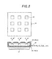
- FIG. 2 it is particularly advantageous to use a housing 14 provided on its front face with many nozzle holes 13, in which convex + poles 15 are arranged on positions matching with the nozzle holes 13, while a frame of the housing 14 is - pole 16 and further a magnet 17 for applying a magnetic field is arranged on a rear face of the housing 14.
- the high bias voltage applying apparatus having the above structure can generate electrons in a good directivity. Therefore, electron beams can be emitted toward desired positions in a good directivity.
- the arranging position of such a high bias voltage applying apparatus is not necessarily limited to the rear face side of the material to be treated.
- the apparatus can be arranged at an irradiation side of depositing ion (Ti ion) and at a side face side of the material 2.
- the bias voltage is about -100 to -3000 V (preferably about -150 to -2000 V). Because, as the bias voltage becomes higher, impact degree of the depositing ion to the steel sheet substrate is strong and the depositing ion deeply penetrate into the steel sheet and hence the adhesion property becomes more excellent.
- an intensity of a magnetic field through a magnetic field generating means is about 50-1000 Gauss.
- bias voltage applying power source it is advantageous to use an arc cut power source or a pulse power source for lessening abnormal discharge in a high plasma atmosphere.
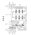
- FIG. 4 is shown a continuous ceramic coating installation of an in-line system suitable for carrying out the invention, which comprises a HDC apparatus incorporated with the above non-contact type high bias voltage applying apparatus, and a magnetron sputtering apparatus.
- a zone (a) is an equipment for installing a grain-oriented silicon steel sheet coil as a material to be treated, which is divided into a preliminary evacuation chamber 19 for previously suctioning the preliminarily installed coil under vacuum and an unwinding chamber 20 for the coil.
- Numeral 21 is a slit, which partitions zone (a) and zone (b).
- the zone (b) is a chamber for forming TiNO coating through the HCD apparatus, at where TiNO coating are formed on both surfaces of the material 2 during the running of the material in an arrow direction.
- Numeral 22 is a deflector roll, and numeral 23 a device for supplying a Ti material.
- a zone (c) is a chamber for forming various ceramic coatings through the magnetron sputtering apparatus, in which numeral 24 is a target, numeral 25 a magnet arranged at a rear side thereof, and numeral 26 a cooling band of the grain-oriented silicon steel sheet after the formation of the ceramic coating.
- a zone (d) is an equipment for discharging the coil after the formation of the ceramic coating, which is divided into a winding chamber 27 of the coil and a discharging chamber 28 thereof.
- FIG. 4 shows a so-called vertical type magnetron sputtering apparatus for conducting the formation of ceramic coating on both surfaces of the steel sheet by vertically arranging the magnetron sputtering apparatuses in two rows. Hover, the magnetron sputtering apparatus is not limitative thereto.
- a so-called lateral type apparatus may be used by laterally arranging the magnetron sputtering apparatuses in two rows.
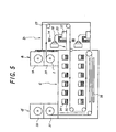
- the magnetron sputtering apparatus is used as a later-stage ion plating apparatus in FIGS. 4 and 5, the otherwise HCD apparatus, P-CVD (Plasma Chemical Vapor Deposition) apparatus, (EB (Electron Beam) + HCD) apparatus and so on may be used in the invention.
- the kind of the ceramic coating formed through the later-stage ion plating apparatus is not particularly limited. Various ceramic coatings including SiN x can be formed.
- a continuously cast slab of silicon steel sheet having a composition comprising of C: 0.076 mass%, Si: 3.35 mass%, Mn: 0.076 mass%, Se: 0.020 mass%, Sb: 0.025 mass%, Al: 0.021 mass%, N: 0.0070 mass% and Mo: 0.012 mass% and the reminder being Fe and inevitable impurities is heated at 1350°C for 4 hours and subjected to hot rolling to obtain a hot rolled sheet having a thickness of 2.0 mm.
- the hot rolled sheet is subjected to a homogenizing at 1050°C for 2 minutes and further to two cold rollings sandwiching an intermediate annealing at 1050°C therebetween to obtain a cold rolled sheet having a final thickness of 0.23 mm.
- the cold rolled sheet is subjected to a decarburization-primary recrystallization annealing in wet H 2 of 840°C, and a slurry of an annealing separator having a composition of MgO (20 mass%), Al 2 O 3 (30 mass%), Sr(OH) (10 mass%), NiCl 3 (15 mass%), CaSiO 3 (5 mass%) and SiO 2 (20 mass%) is applied onto the surface of the steel sheet.
- the decarburization-primary recrystallization annealed sheet is subjected to an annealing at 850°C for 15 hours and the temperature is raised from 850°C to 1100°C at a rate of 12°C/h to develop secondary recrystallized grains strongly accumulated in a Goss orientation, and thereafter subjected to a purification treatment in dry H 2 of 1200°C to produce silicon steel sheet having no forsterite coating.
- an insulating coating composed mainly of a phosphate and colloidal silica is applied and dried, and the sheet is subjected to a baking treatment at 815°C in nitrogen atmosphere for 1 minute and further to a stress relief annealing at 800°C in nitrogen atmosphere for 3 hours.
- the thus obtained grain-oriented silicon steel sheet has the following magnetic properties and adhesion property: B 8 : 1.90T W 17/50 : 0.53 W/kg Adhesion property: no peeling even in 180° bending on a round rod of 15 mm in diameter.
- the grain-oriented silicon steel sheet is produced by the usual production method of grain-oriented steel sheets wherein TiN coating of 0.1 ⁇ m in thickness is pre-coated onto the surface of the non-coating silicon steel sheet by the HCD process without applying bias voltage and SiN x coating of 0.2 ⁇ m in thickness is formed by the magnetron sputtering process and then stress relief annealing is conducted at 800°C in nitrogen atmosphere for 3 hours in a similar manner, and the resulting grain-oriented silicon steel sheet is measured with respect to the magnetic properties and adhesion property to obtain the following results: B 8 : 1.90T W 17/50 : 0.68 W/kg Adhesion property: no peeling even in 180° bending on a round rod of 40 mm in diameter.
- the peeling is not caused in the bending of 15 mm ⁇ as to the adhesion property (minimum diameter causing no peeling even in 180° bending), so that it is noticed that the adhesion property is highly improved as compared with the case of applying no bias voltage.
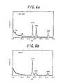
- FIGS. 6a and 6b are results measured by X-ray diffractometry on the ceramic coating obtained by applying a high bias voltage of -200 V and the ceramic coating obtained without applying bias voltage, respectively.
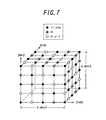
- FIG. 6a In FIG. 6a are observed (111), (200) and (220) peaks of TiN and two peaks at a lower angle side thereof. Such two peaks are considered to be TiNO coating having a crystal structure shown in FIG. 7 from diffraction peaks corresponding to 1/2 and 1/4 positions of the angle of (111) peak, respectively and the result of measurement by GDS (Glow Discharge Spectroscopy).
- any steels having the conventionally known composition are suitable.
- a typical composition is mentioned as follows. C: 0.01-0.08 mass%
- the carbon amount is preferable to be about 0.01-0.08 mass%.
- the silicon amount is preferable to be a range of about 2.0-4.0 mass%.
- Mn is an important component to fix MnS or MnSe as a dispersed precipitation phase exerting on the secondary recrystallization of the grain-oriented silicon steel sheet.
- Mn amount is less than 0.01 mass%, an absolute amount of MnS or the like required for causing the recrystallization is lacking and hence incomplete secondary recrystallization is caused and at the same time surface defect called as blister increases.
- the Mn amount exceeds 0.2 mass%, even if dissociation and solid solution are conducted in the heating of the slab or the like, the dispersed precipitation phase precipitated in the hot rolling is easily coarsened and hence optimum size distribution desired as an inhibitor is damaged to deteriorate the magnetic properties. Therefore, the Mn amount is preferable to be about 0.01-0.2 mass%. S: 0.008-0.1 mass%, Se: 0.003-0.1 mass%
- Each of S and Se is preferable to be not more than 0.1 mass%, and particularly S is a range of 0.008-0.1 mass% and Se is a range of 0.003-0.1 mass%. Because, when each of them exceeds 0.1 mass%, hot and cold workabilities are deteriorated, while when they are less than the lower limits, particular effect is not created in the function of inhibiting the primary grain growth as MnS, MnSe.
- the effect of the invention is not obstructed even if Al, Sb, Cu, B and the like conventionally known as an inhibitor are added together.
- LD converters electric furnaces, open-hearth furnaces and other known steel-making furnaces can be used but also vacuum melting or RH degassing treatment can be combined therewith for the melting of starting materials.
- Any conventionally known methods can be used as a method of adding a slight amount of S, Se or other primary grain growth inhibiting agent included in the starting material to molten steel.
- it can be added to molten steel in the LD converter or at a time of completing RH degassing or in the ingot making.
- the continuously cast slab is heated above 1300°C for dissociating and solid soluting the inhibitors in the slab. Thereafter, the slab is subjected to hot rough rolling and further to hot finish rolling to obtain a hot rolled sheet usually having a thickness of about 1.3-3.3 mm.
- the hot rolled sheet is subjected to a hot rolled sheet annealing (which is also called as homogenizing) within a temperature range of about 850-1100°C, if necessary, and then subjected to one cold rolling or two cold rollings sandwiching an intermediate annealing therebetween up to a final sheet thickness.
- a hot rolled sheet annealing which is also called as homogenizing
- one cold rolling or two cold rollings sandwiching an intermediate annealing therebetween up to a final sheet thickness.
- it is required to watch out for on a final cold rolling reduction (usually 55-90%) for obtaining products having characteristics such as high magnetic flux density and low iron loss.
- an upper limit of the product thickness is 0.5 mm from a viewpoint that eddy current loss of the silicon steel sheet is made small as far as possible, and a lower limit thereof is 0.05 mm for avoiding an adverse effect of hysteresis loss.
- linear recess regions having a width of 50-500 ⁇ m and a depth of 0.1-50 ⁇ m are formed at intervals of 2-10 mm on the surface of the final cold rolled sheet or the steel sheet before or after the secondary recrystallization in a direction cross to the rolling direction.
- the width of the recess region is less than 50 ⁇ m, it is difficult to utilize a demagnetizing field effect, while when it exceeds 500 ⁇ m, the magnetic flux density uneconomically lowers, so that the width of the recess region is limited to a range of 50-500 ⁇ m.
- the demagnetizing field effect can not effectively be utilized, while when it exceeds 50 ⁇ m, the magnetic flux density uneconomically lowers, so that the depth of the recess region is limited to a range of 0.1-50 ⁇ m.
- the forming direction of the linear recess region is optimum to be a direction perpendicular to the rolling direction or a widthwise direction of the sheet, but substantially the same effect can be obtained within a range of ⁇ 30° with respect to the widthwise direction of the sheet.
- a method of forming the linear recess region it is advantageous to use a method wherein an etching resist is applied by printing onto the surface of the final cold rolled sheet and baked and then subjected to an etching treatment and thereafter the resist is removed off.
- This method can be industrially and stably carried out as compared with the conventional method using a blade edge of a knife, a laser or the like, and has an advantage that the iron loss can be reduced more effectively by tensile strength.
- An etching resist ink composed mainly of an alkyd resin is applied onto the surface of the final cold rolled sheet by a gravure off-set printing so as to leave linear non-coated portions having a width of 200 ⁇ m at intervals of 4 mm in a direction substantially perpendicular to the rolling direction and then baked at 200°C for about 20 seconds.
- the thickness of the resist is about 2 ⁇ m.
- the steel sheet coated with the etching resist is subjected to an electrolytic etching or a chemical etching to form linear grooves having a width of 200 ⁇ m and a depth of 20 ⁇ m and then immersed in an organic solvent to remove the resist.
- the electrolytic etching may be carried out in an electrolyte of NaCl at a current density of 10 A/dm 2 for a treating time of about 20 seconds, while the chemical etching may be carried out in a solution of HNO 3 for an immersing time of about 10 seconds.
- the steel sheet is subjected to a decarburization annealing.
- This annealing is conducted in a wet hydrogen atmosphere of, for example, 750-880°C for the purpose that the cold rolled texture is substituted with a primary recrystallization texture and at the same time harmful C in the development of secondary recrystallization grains having ⁇ 110 ⁇ 001> orientation at a final annealing (which is also called as finish annealing) is removed.
- the final annealing is to sufficiently develop the secondary recrystallization grains of ⁇ 110 ⁇ 001> orientation, and is usually carried out by immediately raising a temperature above 1000°C and keeping this temperature through box annealing.
- This final annealing is usually conducted while applying an annealing separator such as magnesia or the like, so that an undercoating called as forsterite is simultaneously formed on the surface.
- an annealing separator such as magnesia or the like
- an including ratio of MgO forming the forsterite undercoating is decreased (not more than 50 mass%), while an including ratio of CaO, Al 2 O 3 , CaSiO 3 , SiO 2 , NiCl 3 , Sr(OH) or the like not forming such an undercoating is increased (not less than 50 mass%).
- a method of annealing by keeping a lower temperature of from 820°C to 900°C is advantageous, but an annealing by gradually heating at a temperature rising rate of about 0.5-15°C/h may be used.
- the steel sheet Since the forsterite undercoating or oxide coating is not basically existent on the surface of the steel sheet after the purification annealing, the steel sheet is directly fed to a subsequent ceramic coating step or subjected to a light pickling treatment before the ceramic coating.
- the invention has a merit that the effect of sufficiently improving the iron loss can be developed after the finish annealing even if a smoothening treatment coming cost-up is not conducted or when the steel sheet is directly fed to the ceramic coating step or to the light pickling treatment before the coating.
- recess grooves can be formed on the surface of the steel sheet.
- the method of forming such grooves may be used the same method as described in the case of applying onto the surface of the final cold rolled sheet or the steel sheet before or after the secondary recrystallization.
- a ceramic coating of TiNO is formed on the surface of the steel sheet as a first coating layer using HCD process having an excellent ionization ratio.
- the thickness of the TiNO pre-coating is about 0.005-0.5 ⁇ m, which is preferable to be about 1/50-1/2 of a total coating thickness (preferably 1/20-1/5).
- the HCD process is an excellent means for ionization of Ti + , in order to form a ceramic coating having an adhesion property, it is also important to ionize reactive gases such as nitrogen, oxygen and the like.
- reactive gases such as nitrogen, oxygen and the like.
- the high bias voltage applying apparatus it is advantageous to use an apparatus capable of promoting the ionization of the reactive gases as shown in FIG. 2.
- ceramic tension coating of one or more layers are formed for increasing the tension applying effect.
- the kind of ceramic tension coating for a second layer or above layers is not particularly limited, but it is preferable to serve as a diffusion barrier in the stress relief annealing at high temperatures.
- SiN x , SiO 2 , CrAlSiN, TiAlN, TiO 2 , CrN and so on are advantageously adaptable.
- the thickness of the ceramic tension coating for the second layer or above layers is preferable to be about 0.05-0.5 ⁇ m in total.
- the magnetron sputtering apparatus is optimum as an apparatus for forming the ceramic tension coating for the second layer or above layers, but HCD apparatus, P-CVD (Plasma Chemical Vapor Deposition) apparatus, EB (Electron Beam) + HCD apparatus and so on may be used.
- a continuously cast slab of silicon steel having a composition of C: 0.075 mass%, Si: 3.43 mass%, Mn: 0.076 mass%, Se: 0.020 mass%, Sb: 0.025 mass%, Al: 0.020 mass%, N: 0.0078 mass%, Mo: 0.012 mass% and the reminder being Fe and inevitable impurities is heated at 1350°C for 4 hours and subjected to a hot rolling to obtain a hot rolled sheet having a thickness of 2.2 mm. Then, the hot rolled sheet is subjected to homogenizing at 1050°C and further to two cold rollings sandwiching an intermediate annealing therebetween at 1000°C to obtain a cold rolled sheet having a final thickness of 0.23 mm.
- the cold rolled sheet is subjected to decarburization-primary recrystallization annealing in a wet H 2 of 840°C, and a slurry of an annealing separator having a composition of MgO (40 mass%), Al 2 O 3 (20 mass%), Sr(OH) (10 mass%), NiCl 3 (10 mass%), CaSiO 3 (5 mass%) and SiO 2 (15 mass%) is applied onto the surface of the steel sheet.
- the decarburization-primary recrystallization annealed sheet is annealed at 850°C for 15 hours and raised from 850° to 1050°C at a rate of 12°C/h to develop secondary recrystallization grains strongly accumulated in a Goss orientation and subjected to purification annealing in a dry H 2 of 1200°C to prepare a non-coating material.
- the thus obtained non-coating silicon steel sheet is directly fed to a continuous ion plating apparatus shown in FIG. 4 to form a ceramic coating of two layers.
- TiNO coating of 0.1 ⁇ m in thickness is first pre-coated by the HCD process under an application of a high-bias voltage of -250 V onto the steel sheet substrate, and then SiN x coating of 0.2 ⁇ m in thickness is formed by the magnetron sputtering process.
- an insulating coating composed mainly of a phosphate and colloidal silica is applied and dried and then subjected to a baking treatment at 815°C in nitrogen atmosphere for 1 minute and further to a stress relief annealing at 800°C in nitrogen atmosphere for 3 hours.
- the thus obtained grain-oriented silicon steel sheet provided with the insulating coating is measured with respect to the magnetic properties and coating adhesion property (180° bending diameter).
- a continuously cast slab of silicon steel having a composition of C: 0.071 mass%, Si: 3.39 mass%, Mn: 0.071 mass%, Se: 0.020 mass%, Sb: 0.025 mass%, Al: 0.021 mass%, N: 0.0079 mass%, Mo: 0.012 mass% and the reminder being Fe and inevitable impurities is heated at 1350°C for 3 hours and subjected to a hot rolling to obtain a hot rolled sheet having a thickness of 2.0 mm. Then, the hot rolled sheet is subjected to homogenizing at 1050°C and further to two cold rollings sandwiching an intermediate annealing at 1050°C to obtain a cold rolled sheet having a thickness of 0.23 mm.
- an etching resist ink composed mainly of an alkyd resin is applied onto the surface of the cold rolled sheet by a gravure off-set printing so as to linearly leave non-applied portions in a direction substantially perpendicular to the rolling direction at a width of 200 ⁇ m and an interval in the rolling direction of 4 mm and baked at 200°C for about 20 seconds.
- the thickness of the resist is 2 ⁇ m.
- the steel sheet coated with the etching resist is subjected to an electrolytic etching to form linear grooves having a width of 200 ⁇ m and a depth of 20 ⁇ m and then immersed in an organic solvent to remove the resist.
- the electrolytic etching is carried out in an electrolyte of NaCl under conditions that a current density is 10 A/dm 2 and a treating time is 20 seconds.
- a slurry of an annealing separator having a composition of MgO (25 mass%), Al 2 O 3 (60 mass%), Si(OH) (10 mass%) and CaSiO 3 (5 mass%) is applied onto the surface of the steel sheet.
- the decarburization-primary recrystallization annealed sheet is annealed at 850°C for 15 hours and raised from 850° to 1100°C at a rate of 12°C/h to develop secondary recrystallization grains strongly accumulated in a Goss orientation and subjected to purification annealing in a dry H 2 of 1220°C to prepare a non-coating material.
- the thus obtained non-coating silicon steel sheet is directly fed to a continuous ion plating apparatus shown in FIG. 5 to form a ceramic coating of two layers.
- TiNO coating of 0.1 ⁇ m in thickness is first pre-coated by the HCD process under an application of a high-bias voltage of -150 V onto the steel sheet substrate, and then SiN x coating of 0.15 ⁇ m in thickness is formed by the magnetron sputtering process.
- an insulating coating composed mainly of a phosphate and colloidal silica is applied and dried and then subjected to a baking treatment at 815°C in nitrogen atmosphere for 1 minute and further to a stress relief annealing at 800°C in nitrogen atmosphere for 3 hours.
- the thus obtained grain-oriented silicon steel sheet provided with the insulating coating is measured with respect to the magnetic properties and coating adhesion property (180° bending diameter).
Landscapes
- Chemical & Material Sciences (AREA)
- Engineering & Computer Science (AREA)
- Materials Engineering (AREA)
- Mechanical Engineering (AREA)
- Metallurgy (AREA)
- Organic Chemistry (AREA)
- Chemical Kinetics & Catalysis (AREA)
- Physics & Mathematics (AREA)
- Electromagnetism (AREA)
- Manufacturing & Machinery (AREA)
- Thermal Sciences (AREA)
- Crystallography & Structural Chemistry (AREA)
- Inorganic Chemistry (AREA)
- Manufacturing Of Steel Electrode Plates (AREA)
- Physical Vapour Deposition (AREA)
- Soft Magnetic Materials (AREA)
- Chemical Treatment Of Metals (AREA)
- Other Surface Treatments For Metallic Materials (AREA)
Abstract
Description
B8: 1.90T
W17/50: 0.53 W/kg
Adhesion property: no peeling even in 180° bending on a round rod of 15 mm in diameter.
B8: 1.90T
W17/50: 0.68 W/kg
Adhesion property: no peeling even in 180° bending on a round rod of 40 mm in diameter.
C: 0.01-0.08 mass%
Therefore, the carbon amount is preferable to be about 0.01-0.08 mass%. Si: 2.0-4.0 mass%
Mn: 0.01-0.2 mass%
S: 0.008-0.1 mass%, Se: 0.003-0.1 mass%
Magnetic flux density B8: 1.90 T
Iron loss W17/50: 0.54 W/kg
Adhesion property: no peeling in bending of 15 mm
Magnetic flux density B8: 1.90 T
Iron loss W17/50: 0.68 W/kg
Adhesion property: no peeling in bending of 50 mm Further, a steel sheet after the pickling treatment of the above non-coating silicon steel sheet and a steel sheet further subjected to a chemical polishing treatment to render the surface into smooth surface are pre-coated with TiNO coating (thickness 0.1 µm) under an application of high bias voltage in the same manner as mentioned above, then SiNx coating (thickness 0.2 µm) is formed through the magnetron sputtering process, further then a phosphate insulating coating is formed thereon, and then subjected to stress relief annealing. The magnetic properties and coating adhesion property (180° bending diameter) are measured with respect to the resultant steel sheets, whereby the following results are obtained.
Magnetic flux density B8: 1.89 T
Iron loss W17/50: 0.60 W/kg
Adhesion property: no peeling in bending of 20 mm
Magnetic flux density B8: 1.91 T
Iron loss W17/50: 0.50 W/kg
Adhesion property: no peeling in bending of 15 mm
Magnetic flux density B8: 1.89 T
Iron loss W17/50: 0.56 W/kg
Adhesion property: no peeling in bending of 20 mm
Magnetic flux density B8: 1.89 T
Iron loss W17/50: 0.70 W/kg
Adhesion property: no peeling in bending of 50 mm Further, a steel sheet after the pickling treatment of the above non-coating silicon steel sheet and a steel sheet further subjected to a chemical polishing treatment to render the surface into smooth surface are pre-coated with TiNO coating (thickness 0.1 µm) under an application of high bias voltage in the same manner as mentioned above, then SiNx coating (thickness 0.01 µm) is formed through the magnetron sputtering process, further then a phosphate insulating coating is formed and then subjected to stress relief annealing. The magnetic properties and coating adhesion property (180° bending diameter) are measured with respect to the resultant steel sheets, whereby the following results are obtained.
Magnetic flux density B8: 1.88 T
Iron loss W17/50: 0.61 W/kg
Adhesion property: no peeling in bending of 25 mm
Magnetic flux density B8: 1.90 T
Iron loss W17/50: 0.49 W/kg
Adhesion property: no peeling in bending of 15 mm
Claims (4)
- An ultra-low iron loss grain-oriented silicon steel sheet having a plurality of ceramic coating layers formed on a surface of a grain-oriented silicon steel sheet after finish annealing, characterized in that said steel sheet has a TiNO coating formed by a hollow cathode discharge process as a first coating layer.
- An ultra-low iron loss grain-oriented silicon steel sheet having a plurality of ceramic coating layers formed on a surface of a grain-oriented silicon steel sheet after finish annealing, characterized in that said steel sheet has a TiNO coating formed by a hollow cathode discharge process as a first coating layer and further a SiNx coating formed by a magnetron sputtering process on the TiNO coating.
- A method of producing an ultra-low iron loss grain-oriented silicon steel sheet by forming a plurality of ceramic coating layers on a surface of a grain-oriented silicon steel sheet after finish annealing without forming a forsterite undercoating on a surface of the steel sheet, characterized in that a TiNO coating is formed on a surface of the as finish annealed steel sheet as a first coating layer by a hollow cathode discharge process under an application of a high bias voltage of not less than -100 V to the steel sheet.
- A method of producing an ultra-low iron loss grain-oriented silicon steel sheet by forming a plurality of ceramic coating layers on a surface of a grain-oriented silicon steel sheet after finish annealing without forming a forsterite undercoating on a surface of the steel sheet, characterized in that a TiNO coating is formed on a surface of the as finish annealed steel sheet as a first coating layer by a hollow cathode discharge process under an application of a high bias voltage of not less than -100 V to the steel sheet and then a SiNx coating is formed on the TiNO coating by a magnetron sputtering process.
Applications Claiming Priority (3)
| Application Number | Priority Date | Filing Date | Title |
|---|---|---|---|
| JP2001159981A JP2002356751A (en) | 2001-05-29 | 2001-05-29 | Ultra-low iron loss unidirectional silicon steel sheet and method for producing the same |
| JP2001159981 | 2001-05-29 | ||
| PCT/JP2002/005219 WO2002097146A1 (en) | 2001-05-29 | 2002-05-29 | Unidirectional silicon steel sheet of ultra-low iron loss and method for production thereof |
Publications (2)
| Publication Number | Publication Date |
|---|---|
| EP1394281A1 true EP1394281A1 (en) | 2004-03-03 |
| EP1394281A4 EP1394281A4 (en) | 2005-12-21 |
Family
ID=19003469
Family Applications (1)
| Application Number | Title | Priority Date | Filing Date |
|---|---|---|---|
| EP02733245A Withdrawn EP1394281A4 (en) | 2001-05-29 | 2002-05-29 | Unidirectional silicon steel sheet of ultra-low iron loss and method for production thereof |
Country Status (6)
| Country | Link |
|---|---|
| US (1) | US6811900B2 (en) |
| EP (1) | EP1394281A4 (en) |
| JP (1) | JP2002356751A (en) |
| KR (1) | KR20030024807A (en) |
| CN (1) | CN1210428C (en) |
| WO (1) | WO2002097146A1 (en) |
Families Citing this family (13)
| Publication number | Priority date | Publication date | Assignee | Title |
|---|---|---|---|---|
| SE0402865L (en) * | 2004-11-04 | 2006-05-05 | Sandvik Intellectual Property | Coated product and method of preparation thereof |
| SE0402904L (en) * | 2004-11-26 | 2006-05-27 | Sandvik Intellectual Property | Coated product and production method for this |
| WO2007075634A2 (en) * | 2005-12-21 | 2007-07-05 | Exxonmobil Research And Engineering Company | Corrosion resistant material for reduced fouling, heat transfer component with improved corrosion and fouling resistance, and method for reducing fouling |
| KR101538778B1 (en) * | 2013-12-24 | 2015-07-22 | 주식회사 포스코 | Grain-oriented electrical steel sheet and method for manufacturing the same |
| CN107849631B (en) * | 2015-07-28 | 2021-12-28 | 杰富意钢铁株式会社 | Linear groove forming method and linear groove forming apparatus |
| KR101762339B1 (en) * | 2015-12-22 | 2017-07-27 | 주식회사 포스코 | Grain oriented electrical steel sheet, and method for manufacturing grain oriented electrical steel sheet |
| SG10202011721TA (en) | 2016-06-02 | 2020-12-30 | Applied Materials Inc | Methods and apparatus for depositing materials on a continuous substrate |
| JP6604463B1 (en) * | 2018-03-30 | 2019-11-13 | Jfeスチール株式会社 | Surface treatment equipment |
| WO2019188976A1 (en) * | 2018-03-30 | 2019-10-03 | Jfeスチール株式会社 | Method for producing grain-oriented electrical steel sheet and continuous film-forming device |
| KR102542947B1 (en) * | 2018-04-25 | 2023-06-14 | 현대자동차주식회사 | Etching method for surface of pvd coated stainless steel |
| DE102018216457A1 (en) * | 2018-09-26 | 2020-03-26 | Thyssenkrupp Ag | Coating of grain-oriented electrical steel by CVD |
| CN113302321A (en) * | 2019-01-16 | 2021-08-24 | 日本制铁株式会社 | Method for producing unidirectional electromagnetic steel sheet |
| EP4240681B1 (en) * | 2020-11-05 | 2025-01-22 | Applied Materials, Inc. | Roll exchange chamber, roll-to-roll processing system and method of continuously providing a flexible substrate |
Family Cites Families (9)
| Publication number | Priority date | Publication date | Assignee | Title |
|---|---|---|---|---|
| EP0193324B1 (en) * | 1985-02-22 | 1989-10-11 | Kawasaki Steel Corporation | Extra-low iron loss grain oriented silicon steel sheets |
| US4863581A (en) * | 1987-02-12 | 1989-09-05 | Kawasaki Steel Corp. | Hollow cathode gun and deposition device for ion plating process |
| JPH0619115B2 (en) * | 1987-05-27 | 1994-03-16 | 川崎製鉄株式会社 | Method for manufacturing ultra low iron loss unidirectional silicon steel sheet |
| EP0307163B1 (en) * | 1987-09-10 | 1993-12-08 | Kawasaki Steel Corporation | Silicon steel sheets having low iron loss and method of producing the same |
| JPH0619115A (en) | 1992-06-30 | 1994-01-28 | Nec Corp | Mask for stepper |
| JPH0673154A (en) | 1992-08-27 | 1994-03-15 | Toshiba Chem Corp | Epoxy resin composition and sealed semiconductor device |
| JPH0673154U (en) * | 1993-03-22 | 1994-10-11 | 川崎製鉄株式会社 | Ion plating device |
| JP2001032055A (en) | 1999-07-19 | 2001-02-06 | Kawasaki Steel Corp | Unidirectional silicon steel sheet excellent in iron loss characteristics and method for producing the same |
| JP2002129309A (en) | 2000-10-24 | 2002-05-09 | Kawasaki Steel Corp | Ultra-low iron loss unidirectional silicon steel sheet without deterioration of iron loss after strain relief annealing and excellent in film adhesion and method for producing the same |
-
2001
- 2001-05-29 JP JP2001159981A patent/JP2002356751A/en active Pending
-
2002
- 2002-05-29 WO PCT/JP2002/005219 patent/WO2002097146A1/en not_active Ceased
- 2002-05-29 KR KR10-2003-7001034A patent/KR20030024807A/en not_active Ceased
- 2002-05-29 EP EP02733245A patent/EP1394281A4/en not_active Withdrawn
- 2002-05-29 CN CNB028025369A patent/CN1210428C/en not_active Expired - Fee Related
- 2002-05-29 US US10/343,206 patent/US6811900B2/en not_active Expired - Lifetime
Also Published As
| Publication number | Publication date |
|---|---|
| CN1464914A (en) | 2003-12-31 |
| JP2002356751A (en) | 2002-12-13 |
| US6811900B2 (en) | 2004-11-02 |
| WO2002097146A1 (en) | 2002-12-05 |
| CN1210428C (en) | 2005-07-13 |
| US20030180554A1 (en) | 2003-09-25 |
| KR20030024807A (en) | 2003-03-26 |
| EP1394281A4 (en) | 2005-12-21 |
Similar Documents
| Publication | Publication Date | Title |
|---|---|---|
| US4698272A (en) | Extra-low iron loss grain oriented silicon steel sheets | |
| RU2721255C1 (en) | Laser-scribed textured silicon steel, which is resistant to stress relieving annealing, and method of its manufacturing | |
| US4713123A (en) | Method of producing extra-low iron loss grain oriented silicon steel sheets | |
| KR101570018B1 (en) | Grain-oriented electrical steel sheet and method for improving iron loss properties thereof | |
| US7169479B2 (en) | Grain-oriented magnetic steel sheet comprising an electrically insulating coating | |
| KR100297046B1 (en) | Very low iron loss oriented electrical steel sheet and its manufacturing method | |
| US6811900B2 (en) | Unidirectional silicon steel sheet of ultra-low iron loss and method for production thereof | |
| US20080271819A1 (en) | Ultra-high magnetic flux density grain-oriented electrical steel sheet excellent in iron loss at a high magnetic flux density and film properties and method for producing the same | |
| EP3530770B1 (en) | Hot-rolled steel sheet for electrical steel sheet production and method of producing same | |
| RU2771318C1 (en) | Method for producing electrical steel sheet with oriented grain structure | |
| US20230175090A1 (en) | Grain-oriented electrical steel sheet, and method for manufacturing grain-oriented electrical steel sheet | |
| KR20190049819A (en) | METHOD FOR MANUFACTURING ORGANIC ELECTRIC STEEL SHEET | |
| JP6660025B2 (en) | Manufacturing method of grain-oriented electrical steel sheet | |
| JPH07320922A (en) | Unidirectional electrical steel sheet with low iron loss | |
| JP2017145490A (en) | Manufacturing method of oriented electromagnetic steel sheet | |
| JP7006851B1 (en) | Directional electrical steel sheet and its manufacturing method | |
| JP7375670B2 (en) | Grain-oriented electrical steel sheet and its manufacturing method | |
| RU2768094C1 (en) | Method for producing electrotechnical steel sheet with oriented grain structure | |
| WO2018116829A1 (en) | Grain-oriented electrical steel sheet and production method for grain-oriented electrical steel sheet | |
| JPH11286775A (en) | Method for producing ultra-low iron loss unidirectional silicon steel sheet | |
| RU2861182C2 (en) | Grain-oriented electrical steel sheet and method for manufacturing same | |
| EP4624616A1 (en) | Grain-oriented electrical steel sheet and manufacturing method therefor | |
| JP2003342699A (en) | Method for producing ultra-low iron loss unidirectional silicon steel sheet with excellent coating adhesion and no deterioration in properties after strain relief annealing | |
| JP4042202B2 (en) | Unidirectional silicon steel sheet | |
| US20250188560A1 (en) | Method for manufacturing grain-oriented electrical steel sheet, and grain-oriented electrical steel sheet |
Legal Events
| Date | Code | Title | Description |
|---|---|---|---|
| PUAI | Public reference made under article 153(3) epc to a published international application that has entered the european phase |
Free format text: ORIGINAL CODE: 0009012 |
|
| 17P | Request for examination filed |
Effective date: 20030116 |
|
| AK | Designated contracting states |
Kind code of ref document: A1 Designated state(s): AT BE CH CY DE DK ES FI FR GB GR IE IT LI LU MC NL PT SE TR |
|
| A4 | Supplementary search report drawn up and despatched |
Effective date: 20051108 |
|
| RIC1 | Information provided on ipc code assigned before grant |
Ipc: 7C 22C 38/00 A Ipc: 7C 23C 14/22 B Ipc: 7C 23C 28/04 B Ipc: 7C 23C 14/02 B Ipc: 7C 23C 14/06 B |
|
| 17Q | First examination report despatched |
Effective date: 20091103 |
|
| STAA | Information on the status of an ep patent application or granted ep patent |
Free format text: STATUS: THE APPLICATION IS DEEMED TO BE WITHDRAWN |
|
| 18D | Application deemed to be withdrawn |
Effective date: 20100514 |