EP1388976A1 - System and method for implementing auto-configurable default polarity - Google Patents
System and method for implementing auto-configurable default polarity Download PDFInfo
- Publication number
- EP1388976A1 EP1388976A1 EP03017847A EP03017847A EP1388976A1 EP 1388976 A1 EP1388976 A1 EP 1388976A1 EP 03017847 A EP03017847 A EP 03017847A EP 03017847 A EP03017847 A EP 03017847A EP 1388976 A1 EP1388976 A1 EP 1388976A1
- Authority
- EP
- European Patent Office
- Prior art keywords
- polarity
- transceiver
- default
- module
- selection
- Prior art date
- Legal status (The legal status is an assumption and is not a legal conclusion. Google has not performed a legal analysis and makes no representation as to the accuracy of the status listed.)
- Granted
Links
- 238000000034 method Methods 0.000 title claims abstract description 17
- 230000003287 optical effect Effects 0.000 claims description 10
- 239000010410 layer Substances 0.000 description 32
- 238000010586 diagram Methods 0.000 description 9
- 238000004891 communication Methods 0.000 description 8
- 230000005540 biological transmission Effects 0.000 description 3
- 239000000835 fiber Substances 0.000 description 3
- 230000002411 adverse Effects 0.000 description 2
- 230000008901 benefit Effects 0.000 description 2
- 238000011084 recovery Methods 0.000 description 2
- RYGMFSIKBFXOCR-UHFFFAOYSA-N Copper Chemical compound [Cu] RYGMFSIKBFXOCR-UHFFFAOYSA-N 0.000 description 1
- 238000013459 approach Methods 0.000 description 1
- 230000015556 catabolic process Effects 0.000 description 1
- 230000008859 change Effects 0.000 description 1
- 238000006243 chemical reaction Methods 0.000 description 1
- 239000010949 copper Substances 0.000 description 1
- 229910052802 copper Inorganic materials 0.000 description 1
- 238000013500 data storage Methods 0.000 description 1
- 238000006731 degradation reaction Methods 0.000 description 1
- 238000001514 detection method Methods 0.000 description 1
- 229910003460 diamond Inorganic materials 0.000 description 1
- 239000010432 diamond Substances 0.000 description 1
- 239000002346 layers by function Substances 0.000 description 1
- 238000007726 management method Methods 0.000 description 1
- 238000004519 manufacturing process Methods 0.000 description 1
- 239000000463 material Substances 0.000 description 1
- 238000012986 modification Methods 0.000 description 1
- 230000004048 modification Effects 0.000 description 1
- 239000013307 optical fiber Substances 0.000 description 1
- 230000004044 response Effects 0.000 description 1
Images


Classifications
-
- H—ELECTRICITY
- H04—ELECTRIC COMMUNICATION TECHNIQUE
- H04L—TRANSMISSION OF DIGITAL INFORMATION, e.g. TELEGRAPHIC COMMUNICATION
- H04L12/00—Data switching networks
- H04L12/28—Data switching networks characterised by path configuration, e.g. LAN [Local Area Networks] or WAN [Wide Area Networks]
- H04L12/40—Bus networks
- H04L12/40006—Architecture of a communication node
- H04L12/40032—Details regarding a bus interface enhancer
-
- H—ELECTRICITY
- H04—ELECTRIC COMMUNICATION TECHNIQUE
- H04L—TRANSMISSION OF DIGITAL INFORMATION, e.g. TELEGRAPHIC COMMUNICATION
- H04L49/00—Packet switching elements
- H04L49/35—Switches specially adapted for specific applications
- H04L49/351—Switches specially adapted for specific applications for local area network [LAN], e.g. Ethernet switches
- H04L49/352—Gigabit ethernet switching [GBPS]
-
- H—ELECTRICITY
- H04—ELECTRIC COMMUNICATION TECHNIQUE
- H04L—TRANSMISSION OF DIGITAL INFORMATION, e.g. TELEGRAPHIC COMMUNICATION
- H04L49/00—Packet switching elements
- H04L49/35—Switches specially adapted for specific applications
- H04L49/356—Switches specially adapted for specific applications for storage area networks
- H04L49/357—Fibre channel switches
Definitions
- Embodiments of the present invention relate generally to a method and system for implementing polarity for a single chip.
- High-speed digital communication networks over copper and optical fiber are used in many network communication and digital storage applications.
- Ethemet and Fiber Channels are two widely used communication protocols that continue to evolve in response to the increasing need for higher bandwidth in digital communication systems.
- the Open Systems Interconnection (alternatively referred to as the "OSI") model (ISO standard) was developed to establish standardization for linking heterogeneous computer and communication systems.
- the OSI model includes seven distinct functional layers including Layer 7: an application layer; Layer 6: a presentation layer; Layer 5: a session layer; Layer 4: a transport layer; Layer 3: a network layer; Layer 2: a data link layer; and Layer 1: a physical layer.
- Each OSI layer is responsible for establishing what is to be done at that layer of the network but not how to implement it.
- Layers 1 to 4 handle network control, and data transmission and reception.
- Layers 5 to 7 handle application issues. It is contemplated that specific functions of each layer may vary to a certain extent, depending on the exact requirements of a given protocol to be implemented for that layer. For example, the Ethernet protocol provides collision detection and carrier sensing in the physical layer.
- the physical layer (i.e., Layer 1) is responsible for handling all electrical, optical, and mechanical requirements for interfacing to the communication media.
- the physical layer provides encoding and decoding, synchronization, clock data recovery, and transmission and reception of bit streams.
- high-speed electrical or optical transceivers are the hardware elements used to implement such layer.
- An optical-based transceiver for example, includes various functional components such as clock data recovery, clock multiplication, serialization/deserialization, encoding/decoding, electrical/optical conversion, descrambling, media access control, controlling, and data storage. Many of the functional components are often implemented in separate IC chips.
- transceivers may have a different polarity from the devices or upper level systems with which they are associated (alternatively referred to as "associated devices"). Such different polarities must be accommodated.
- Some solutions have included inserting one or more chips between the transceiver and the associated devices (or software) to reconfigure the polarity. It is contemplated that inserting such a chip may affect production cost and time. Furthermore, such chips may not work correctly, adversely affecting the communication between the transceiver and the associated devices.
- Another solution involves making at least two versions of the transceiver, a first version having one polarity, and a second version having the opposite polarity. It is contemplated that this solution is susceptible to error, in that the wrong version of the transceiver may be used, adversely affecting communication between the transceiver and the associated devices.
- a further solution involves the crossing of signal paths to achieve correct polarity. This solution, however, results in signal degradation.
- One embodiment of the present invention relates to a system and method for implementing auto-configurable default polarity.
- the single chip multi-sublayer PHY comprises at least one selection register adapted to store at least one default polarity setting and at least one selection module communicating with at least the selection register and adapted to select one polarity from at least two possible polarities based at least in part on the default polarity setting.
- the selection module of the single chip multi-sublayer PHY comprises at least one multiplexer.
- This embodiment may further comprise an inverter coupled to at least the selection module.
- At least one differential driver may be coupled to the selection device having at least one output interface coupled thereto.
- This embodiment may further comprise a polarity override interface communicating with the selection register and adapted to communicate an override signal thereto.
- the embodiment may comprise at least one program module or EEPROM coupled to the selection register.
- transceiver comprises at least one program module adapted to be programmed with at least a default polarity setting and a single chip multi-sublayer PHY.
- the single chip multi-sublayer PHY comprises at least one selection register communicating with at least the program module and at least one selection module communicating with at least the selection register.
- the selection register is adapted to store at least the default polarity setting, while the selection module is adapted to select one polarity from at least two possible polarities based at least in part on the default polarity setting.
- Yet another embodiment of the present invention relates to a method of configuring a polarity for a transceiver module.
- the embodiment comprises writing a default polarity into at least one programming module, writing or storing the default polarity into at least one selection register on a single chip multi-sublayer PHY and selecting the polarity from at least two possible polarities using at least the default polarity.
- This embodiment may also comprise overriding the default polarity and selecting the polarity from at least two possible polarities using at least the overridden default polarity
- Fig. 1 illustrates a schematic block diagram illustrating certain components of a Gigabit transceiver module, generally designated 5, with a XAUI interface 15 in accordance with an embodiment of the present invention.
- the transceiver module 5 may, in one embodiment of the present invention, be compatible with the XENPAK optical module standard.
- the transceiver module 5 includes, for example, a single-chip multi-sublayer PHY 10, an optical PMD 30, and an EEPROM 40.
- a media access controller (alternatively referred to as "MAC") 20 interfaces to the single-chip multi-sublayer PHY 10 through the XAUI transmit and receive interface 15.
- the MAC layer comprises one of two sublayers of the data link control layer and is concerned with sharing the physical connection to a network among several upper-level systems.
- the single-chip multi-sublayer PHY 10 interfaces to the optical PMD 30 through a PMD transmit and receive interface 17.
- the MAC 20 also interfaces to the single-chip multi-sublayer PHY 10 through the serial management data input/output (alternatively referred to as an "MDIO") interface 16.
- MDIO serial management data input/output
- the single-chip multi-sublayer PHY 10 also interfaces to EEPROM 40 through a two-wire serial interface 19. In this embodiment, a XGMII interface is not used.
- the XAUI interface 15 comprises 4 channels of 3 Gigabit serial data received by the single-chip multi-sublayer PHY 10 from the MAC 20 and 4 channels of 3 Gigabit serial data transmitted from the single-chip multi-sublayer PHY 10 to the MAC 20.
- the MAC 20 includes a XGXS sublayer interface 21 and a reconciliation sublayer or RS interface 22.
- the 3 Gigabit data rate is actually 3.125 Gbps and for Fibre Channel operation for example, the 3 Gigabit data rate is actually 3.1875 Gbps.
- the PMD interface 17 comprises a 10 Gigabit serial transmit differential interface and a 10 Gigabit serial receive differential interface between the single-chip multi-sublayer PHY 10 and the optical PMD 30 in accordance with an embodiment of the present invention.
- the 10 Gigabit data rate is actually 10.3125 Gbps and for Fibre Channel operation for example, the 10 Gigabit data rate is actually 10.516 Gbps.
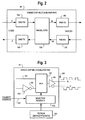
- Fig. 2 illustrates a schematic block diagram of the single-chip multi-sublayer PHY 10 used in the transceiver module 5 of Fig. 1 in accordance with an embodiment of the present invention.
- the single-chip multi-sublayer PHY 10 comprises a PMD transmit (alternatively referred to as "TX") module 110, a PMD receive (alternatively referred to as "RX") module 120, a digital core module 130, a XAUI transmit or TX section 140, and a XAUI receive or RX module 150.
- TX PMD transmit
- RX PMD receive
- a transceiver module (similar to those provided above, for example) includes a single chip multi-sublayer PHY adapted to implement auto-configurable default polarity.
- Fig. 3 illustrates one embodiment of the present invention comprising at least one program module adapted to be programmed with at least a default polarity setting.
- the program module may comprise an EEPROM 160 that is adapted to be programmed with one or more default polarity settings. While an EEPROM is discussed, other program modules are contemplated.
- the EEPROM may be on the single chip multi-sublayer PHY or otherwise on the transceiver module, or outside the transceiver module but in the upper level system. It may be desirable to program the EEPROM in a given transceiver module such that the programmed polarity is compatible with the particular customer that will use the given transceiver module.
- the program module communicates with at least one selection register 170, where the selection register is adapted to store at least the default polarity setting.
- the default polarity setting is programmed or written into the EEPROM 160. Upon start-up, such default polarity setting is communicated to the selection register 170.
- One embodiment of the single chip multi-sublayer PHY further comprises at least one selection module or device 180 (for example, a multiplexer or mux) communicating with at least the selection register 170 and adapted to select at least one polarity from at least two possible polarities based at least in part on the default polarity setting.
- at least two signals 191 and 192 having different polarities are communicated to the mux 180.
- signal 191 is selected by the mux 180.
- signal 192 is selected by the mux 180.
- an inverter 193 is shown coupled to the mux 180, such that the second polarity is the inverse or opposite of the first polarity, although other relationships between the two signals and their respective polarities is contemplated.
- a differential driver 195 is illustrated communicating with the mux 180 and an output interface 196 (a differential twisted pair for example).
- Fig. 3 further illustrates a polarity override interface 197 coupled to and communicating with the selection register 170.
- the polarity interface enables overriding of the default polarity setting stored in the selection register, such that a different polarity may be used. It is also contemplated that, in one embodiment, a different polarity setting may be programmed into the program module or EEPROM 160 and communicated to the selection register 170.
- Fig. 4 illustrates a high level flow diagram illustrating one embodiment of the present invention relating to a method, generally designated 200, for auto-configuring a polarity (for a transceiver module for example) using a single chip multi-sublayer PHY, for example.
- This embodiment comprises programming a default polarity using at least one programming module and writing the default polarity into at least one selection register on the single chip multi-sublayer PHY as illustrated by blocks 210 and 212 respectively.
- the single chip multi-sublayer PHY selects the polarity from at least two possible polarities using at least the default polarity as illustrated by block 214.
- the mux selects the first signal. If at the output, the default polarity corresponds to a second signal (signal 192 for example) the mux selects the second signal.
- Fig. 5 illustrates a detailed flow diagram of a method, generally designated 300, for auto-configuring a polarity using, for example, a single chip multi-sublayer PHY in accordance with one embodiment of the present invention.
- This embodiment comprises writing one or more default polarity settings into the program module as illustrated by block 310.
- the default polarity setting is programmed or written into the program module or EEPROM.
- Upon start-up, such default polarity setting is communicated to at least one selection register as illustrated by block 312, where the selection register is adapted to store at least the default polarity setting.
- method 300 determines whether the default polarity settings are used by an associated device as illustrated by diamond 314.
- a user e.g., a customer desiring to couple the transceiver module of the present invention to an associated device
- the default polarity settings is used by the associated device, the default polarity is overridden such that a different polarity setting may be communicated and stored in the at least one selection register as illustrated by block 320.
- the user may modify the default polarity so that it corresponds to the polarity of the associated device.
- the polarity override coupled to and communicating with the selection register is used to override the default setting.
- the selection device or module e.g., the mux communicating with at least the selection register, selects another polarity from the possible polarities as illustrated by block 322.
Landscapes
- Engineering & Computer Science (AREA)
- Computer Networks & Wireless Communication (AREA)
- Signal Processing (AREA)
- Communication Control (AREA)
- Information Transfer Systems (AREA)
- Dc Digital Transmission (AREA)
- Logic Circuits (AREA)
Abstract
Description
Claims (20)
- PHY system comprising:at least one selection register adapted to store at least one default polarity setting; andat least one selection module communicating with said at least one selection register and adapted to select at least one polarity from at least two possible polarities based at least in part on said default polarity setting.
- The system of Claim 1, wherein said selection module comprises at least one multiplexer.
- The system of Claim 1 comprising an inverter coupled to at least said selection module.
- The system of Claim 1 comprising a differential driver coupled to said selection module.
- The system of Claim 4 comprising at least one output interface coupled to at least said differential driver.
- The system of Claim 1 comprising a polarity override interface communicating with said selection register and adapted to communicate an override signal thereto.
- The system of Claim 1, further comprising at least one program module coupled to said selection register.
- The system of Claim 7, wherein said at least one program module comprises an EEPROM.
- A transceiver comprising:at least one program module adapted to be programmed with at least a default polarity setting; anda PHY comprising:at least one selection register communicating with at least said program module, said selection register adapted to store at least said default polarity setting; andat least one selection module communicating with said at least one selection register and adapted to select at least one polarity from at least two possible polarities based at least in part on said default polarity setting.
- The transceiver of Claim 9, comprising at least one optical PMD communicating with said PHY.
- The transceiver of Claim 10, comprising at least one PMD transmit and receive interface coupled to said optical PMD and said PHY.
- The transceiver of Claim 11, wherein said PMD transmit and receive interface comprises a 10 Gigabit serial transmit differential interface and a 10 Gigabit serial receive differential interface.
- The transceiver of Claim 9, wherein said at least one selection module comprises a multiplexer.
- The transceiver of Claim 9 comprising an inverter coupled to at least said selection module.
- The transceiver of Claim 9 comprising a differential driver coupled to said selection module.
- The transceiver of Claim 15 comprising at least one output interface coupled to at least said differential driver.
- The transceiver of Claim 9 comprising a polarity override interface communicating with said selection register and adapted to communicate an override signal thereto.
- A method of configuring a polarity for a transceiver module comprising:writing a default polarity into at least one programming module;storing said default polarity into at least one selection register on a PHY; andselecting a polarity from at least two possible polarities using at least said default polarity.
- The method of Claim 18 comprising overriding said default polarity.
- The method of Claim 19 comprising selecting the polarity from at least two possible polarities using at least said overridden default polarity
Applications Claiming Priority (4)
| Application Number | Priority Date | Filing Date | Title |
|---|---|---|---|
| US372158 | 1982-04-26 | ||
| US40209602P | 2002-08-07 | 2002-08-07 | |
| US402096P | 2002-08-07 | ||
| US10/372,158 US7656893B2 (en) | 2002-08-07 | 2003-02-21 | System and method for implementing auto-configurable default polarity |
Publications (2)
| Publication Number | Publication Date |
|---|---|
| EP1388976A1 true EP1388976A1 (en) | 2004-02-11 |
| EP1388976B1 EP1388976B1 (en) | 2008-07-02 |
Family
ID=30448283
Family Applications (1)
| Application Number | Title | Priority Date | Filing Date |
|---|---|---|---|
| EP03017847A Expired - Lifetime EP1388976B1 (en) | 2002-08-07 | 2003-08-05 | System and method for implementing auto-configurable default polarity |
Country Status (3)
| Country | Link |
|---|---|
| US (2) | US7656893B2 (en) |
| EP (1) | EP1388976B1 (en) |
| DE (1) | DE60321869D1 (en) |
Cited By (1)
| Publication number | Priority date | Publication date | Assignee | Title |
|---|---|---|---|---|
| US12277351B1 (en) * | 2022-11-30 | 2025-04-15 | Suzhou Metabrain Intelligent Technology Co., Ltd. | Polarity inversion method and apparatus, storage medium and electronic apparatus |
Citations (2)
| Publication number | Priority date | Publication date | Assignee | Title |
|---|---|---|---|---|
| US6049837A (en) * | 1997-12-08 | 2000-04-11 | International Business Machines Corporation | Programmable output interface for lower level open system interconnection architecture |
| US6215816B1 (en) * | 1997-03-04 | 2001-04-10 | Texas Instruments Incorporated | Physical layer interface device |
Family Cites Families (10)
| Publication number | Priority date | Publication date | Assignee | Title |
|---|---|---|---|---|
| US4717912A (en) * | 1982-10-07 | 1988-01-05 | Advanced Micro Devices, Inc. | Apparatus for producing any one of a plurality of signals at a single output |
| JP2915945B2 (en) * | 1990-01-12 | 1999-07-05 | 株式会社アドバンテスト | Memory test equipment |
| US5386155A (en) * | 1993-03-30 | 1995-01-31 | Intel Corporation | Apparatus and method for selecting polarity and output type in a programmable logic device |
| US5553070A (en) * | 1994-09-13 | 1996-09-03 | Riley; Robert E. | Data link module for time division multiplexing control systems |
| US5635856A (en) * | 1995-10-03 | 1997-06-03 | Cypress Semiconductor Corporation | High speed programmable macrocell with combined path for storage and combinatorial modes |
| JP3395760B2 (en) * | 1999-06-01 | 2003-04-14 | セイコーエプソン株式会社 | Voltage generation method, electro-optical device, and electronic apparatus |
| US6944163B2 (en) * | 2000-02-09 | 2005-09-13 | Nortel Networks Limited | 10 Gigabit ethernet mappings for a common LAN/WAN PMD interface with a simple universal physical medium dependent interface |
| US6606670B1 (en) * | 2000-08-16 | 2003-08-12 | Microchip Technology Incorporated | Circuit serial programming of default configuration |
| US7020729B2 (en) * | 2002-05-16 | 2006-03-28 | Intel Corporation | Protocol independent data transmission interface |
| US7111208B2 (en) * | 2002-10-02 | 2006-09-19 | Broadcom Corporation | On-chip standalone self-test system and method |
-
2003
- 2003-02-21 US US10/372,158 patent/US7656893B2/en not_active Expired - Fee Related
- 2003-08-05 EP EP03017847A patent/EP1388976B1/en not_active Expired - Lifetime
- 2003-08-05 DE DE60321869T patent/DE60321869D1/en not_active Expired - Lifetime
-
2009
- 2009-12-22 US US12/644,917 patent/US8767761B2/en not_active Expired - Fee Related
Patent Citations (2)
| Publication number | Priority date | Publication date | Assignee | Title |
|---|---|---|---|---|
| US6215816B1 (en) * | 1997-03-04 | 2001-04-10 | Texas Instruments Incorporated | Physical layer interface device |
| US6049837A (en) * | 1997-12-08 | 2000-04-11 | International Business Machines Corporation | Programmable output interface for lower level open system interconnection architecture |
Cited By (1)
| Publication number | Priority date | Publication date | Assignee | Title |
|---|---|---|---|---|
| US12277351B1 (en) * | 2022-11-30 | 2025-04-15 | Suzhou Metabrain Intelligent Technology Co., Ltd. | Polarity inversion method and apparatus, storage medium and electronic apparatus |
Also Published As
| Publication number | Publication date |
|---|---|
| DE60321869D1 (en) | 2008-08-14 |
| EP1388976B1 (en) | 2008-07-02 |
| US7656893B2 (en) | 2010-02-02 |
| US20040037119A1 (en) | 2004-02-26 |
| US8767761B2 (en) | 2014-07-01 |
| US20100098141A1 (en) | 2010-04-22 |
Similar Documents
| Publication | Publication Date | Title |
|---|---|---|
| US7068609B2 (en) | Method and apparatus for performing wire speed auto-negotiation | |
| US8473640B2 (en) | System and method for implementing a single chip having a multiple sub-layer PHY | |
| US9614776B1 (en) | Systems and methods for transmitting data according to an auto-negotiated data rate | |
| US6859825B1 (en) | System and method enabling configuration of physical layer devices and corresponding link partners for communicating network data via a configuration source or auto-negotiation | |
| US6115389A (en) | Auto-negotiation for multiple ports using shared logic | |
| CN101039148B (en) | Optical module and method and network equipment for supporting GE optical connector and FE optical connector | |
| US20040208180A1 (en) | System and method for supporting auto-negotiation among standards having different rates | |
| US20100115316A1 (en) | Method and system for managing energy efficiency of a network link via pluggable transceiver modules in an energy efficient network device | |
| US7957283B2 (en) | Multi-port ethernet transceiver | |
| US9807036B2 (en) | Apparatus and method for encoding MDIO into SGMII transmissions | |
| US20130336145A1 (en) | Method and system for a plurality of physical layers for network connection | |
| US7668194B2 (en) | Dual speed interface between media access control unit and physical unit | |
| EP1471705A1 (en) | A means and control method for adapting different media of transmission link of network on physical layer. | |
| US6507591B1 (en) | Handshaking between repeater and physical layer device in a variable rate network transceiver | |
| US6906426B2 (en) | Transceiver having shadow memory facilitating on-transceiver collection and communication of local parameters | |
| CN108809861A (en) | File transmitting method and message method of reseptance and device | |
| US8767761B2 (en) | Implementing auto-configurable default polarity | |
| WO2025247264A1 (en) | Method, apparatus and system for negotiating operating mode of optical module | |
| PHY | Transceiver Configurations in Arria V GZ Devices | |
| CN111258945A (en) | Embedded system communication interface and communication method | |
| Rockrohr | Overview of Protocol Standards |
Legal Events
| Date | Code | Title | Description |
|---|---|---|---|
| PUAI | Public reference made under article 153(3) epc to a published international application that has entered the european phase |
Free format text: ORIGINAL CODE: 0009012 |
|
| AK | Designated contracting states |
Kind code of ref document: A1 Designated state(s): AT BE BG CH CY CZ DE DK EE ES FI FR GB GR HU IE IT LI LU MC NL PT RO SE SI SK TR |
|
| AX | Request for extension of the european patent |
Extension state: AL LT LV MK |
|
| 17P | Request for examination filed |
Effective date: 20040811 |
|
| AKX | Designation fees paid |
Designated state(s): DE FR GB |
|
| RAP1 | Party data changed (applicant data changed or rights of an application transferred) |
Owner name: BROADCOM CORPORATION |
|
| GRAP | Despatch of communication of intention to grant a patent |
Free format text: ORIGINAL CODE: EPIDOSNIGR1 |
|
| GRAS | Grant fee paid |
Free format text: ORIGINAL CODE: EPIDOSNIGR3 |
|
| GRAA | (expected) grant |
Free format text: ORIGINAL CODE: 0009210 |
|
| AK | Designated contracting states |
Kind code of ref document: B1 Designated state(s): DE FR GB |
|
| REG | Reference to a national code |
Ref country code: GB Ref legal event code: FG4D |
|
| REF | Corresponds to: |
Ref document number: 60321869 Country of ref document: DE Date of ref document: 20080814 Kind code of ref document: P |
|
| PLBE | No opposition filed within time limit |
Free format text: ORIGINAL CODE: 0009261 |
|
| STAA | Information on the status of an ep patent application or granted ep patent |
Free format text: STATUS: NO OPPOSITION FILED WITHIN TIME LIMIT |
|
| 26N | No opposition filed |
Effective date: 20090403 |
|
| REG | Reference to a national code |
Ref country code: FR Ref legal event code: ST Effective date: 20090630 |
|
| PG25 | Lapsed in a contracting state [announced via postgrant information from national office to epo] |
Ref country code: FR Free format text: LAPSE BECAUSE OF NON-PAYMENT OF DUE FEES Effective date: 20080901 |
|
| PGFP | Annual fee paid to national office [announced via postgrant information from national office to epo] |
Ref country code: GB Payment date: 20130823 Year of fee payment: 11 |
|
| GBPC | Gb: european patent ceased through non-payment of renewal fee |
Effective date: 20140805 |
|
| PG25 | Lapsed in a contracting state [announced via postgrant information from national office to epo] |
Ref country code: GB Free format text: LAPSE BECAUSE OF NON-PAYMENT OF DUE FEES Effective date: 20140805 |
|
| REG | Reference to a national code |
Ref country code: DE Ref legal event code: R082 Ref document number: 60321869 Country of ref document: DE Representative=s name: BOSCH JEHLE PATENTANWALTSGESELLSCHAFT MBH, DE Ref country code: DE Ref legal event code: R081 Ref document number: 60321869 Country of ref document: DE Owner name: AVAGO TECHNOLOGIES INTERNATIONAL SALES PTE. LT, SG Free format text: FORMER OWNER: BROADCOM CORP., IRVINE, CALIF., US Ref country code: DE Ref legal event code: R081 Ref document number: 60321869 Country of ref document: DE Owner name: AVAGO TECHNOLOGIES GENERAL IP (SINGAPORE) PTE., SG Free format text: FORMER OWNER: BROADCOM CORP., IRVINE, CALIF., US |
|
| REG | Reference to a national code |
Ref country code: DE Ref legal event code: R082 Ref document number: 60321869 Country of ref document: DE Representative=s name: BOSCH JEHLE PATENTANWALTSGESELLSCHAFT MBH, DE Ref country code: DE Ref legal event code: R081 Ref document number: 60321869 Country of ref document: DE Owner name: AVAGO TECHNOLOGIES INTERNATIONAL SALES PTE. LT, SG Free format text: FORMER OWNER: AVAGO TECHNOLOGIES GENERAL IP (SINGAPORE) PTE. LTD., SINGAPORE, SG |
|
| PGFP | Annual fee paid to national office [announced via postgrant information from national office to epo] |
Ref country code: DE Payment date: 20200831 Year of fee payment: 18 |
|
| REG | Reference to a national code |
Ref country code: DE Ref legal event code: R119 Ref document number: 60321869 Country of ref document: DE |
|
| PG25 | Lapsed in a contracting state [announced via postgrant information from national office to epo] |
Ref country code: DE Free format text: LAPSE BECAUSE OF NON-PAYMENT OF DUE FEES Effective date: 20220301 |