EP1388890A1 - Method for manufacturing electronic component - Google Patents
Method for manufacturing electronic component Download PDFInfo
- Publication number
- EP1388890A1 EP1388890A1 EP03703043A EP03703043A EP1388890A1 EP 1388890 A1 EP1388890 A1 EP 1388890A1 EP 03703043 A EP03703043 A EP 03703043A EP 03703043 A EP03703043 A EP 03703043A EP 1388890 A1 EP1388890 A1 EP 1388890A1
- Authority
- EP
- European Patent Office
- Prior art keywords
- substrate
- front surface
- gas
- etching
- dry
- Prior art date
- Legal status (The legal status is an assumption and is not a legal conclusion. Google has not performed a legal analysis and makes no representation as to the accuracy of the status listed.)
- Withdrawn
Links
Images










Classifications
-
- G—PHYSICS
- G01—MEASURING; TESTING
- G01C—MEASURING DISTANCES, LEVELS OR BEARINGS; SURVEYING; NAVIGATION; GYROSCOPIC INSTRUMENTS; PHOTOGRAMMETRY OR VIDEOGRAMMETRY
- G01C19/00—Gyroscopes; Turn-sensitive devices using vibrating masses; Turn-sensitive devices without moving masses; Measuring angular rate using gyroscopic effects
- G01C19/56—Turn-sensitive devices using vibrating masses, e.g. vibratory angular rate sensors based on Coriolis forces
- G01C19/5607—Turn-sensitive devices using vibrating masses, e.g. vibratory angular rate sensors based on Coriolis forces using vibrating tuning forks
-
- H—ELECTRICITY
- H10—SEMICONDUCTOR DEVICES; ELECTRIC SOLID-STATE DEVICES NOT OTHERWISE PROVIDED FOR
- H10P—GENERIC PROCESSES OR APPARATUS FOR THE MANUFACTURE OR TREATMENT OF DEVICES COVERED BY CLASS H10
- H10P52/00—Grinding, lapping or polishing of wafers, substrates or parts of devices
Definitions
- the present invention relates to a method of manufacturing an electronic device including an electronic element formed on a planer substrate, such as a silicon substrate and a glass substrate.
- An electronic device is generally manufactured by forming layers of metal, dielectric, and semiconductor materials on a planer substrate, such as a silicon substrate and a glass substrate sequentially and by patterning the layers. Plural electronic elements are formed simultaneously on the substrate. Then, conventionally, the substrate is divided into chips including electronic elements by, e.g., a dicing blade, respectively. The electronic elements are separated, thus causing the device to be manufactured at a low productivity.
- An electronic circuit is manufactured by the following method.
- An element is formed on a front surface of a substrate, and a recess is provided around the element in the front surface of the substrate. A portion of the substrate is removed from the back surface of the substrate until reaching the recess.
- the elements is separated simultaneously by removing a portion of the substrate from the back surface of the substrate, thus improving efficiency of the production of the device.
- Fig. 1 is a perspective view of an angular rate sensor as an electronic element according to exemplary embodiments of the present invention.
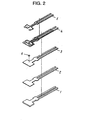
- Fig. 2 is an exploded perspective view of the element.
- a buffer layer 2, a lower electrode layer 3, a piezoelectric layer 4, an upper electrode layer 5, and an auxiliary electrode 6 are provided in a sequence on a substrate 1 having a tuning fork shape.
- the upper electrode layer 5 consists of an oscillator electrode 5A and a detector electrode 5B which face the piezoelectric layer 4 across the lower electrode 3.
- the piezoelectric layer 4 provided between the oscillator electrode 5A and the lower electrode 3 expands and contracts to deflect arms 10A and 10B provided in the substrate 1, hence triggering an oscillation of the tuning fork in a lateral direction.
- the arms 10A and 10B deflect in a direction perpendicular to the axis A and the direction of the oscillation.
- the deflection generates an electrical charge in the piezoelectric layer 4 according to the amount of the deflection.
- the electric charge is then measured through the detector electrode 5B and translated into the angular rate.
- FIG. 3 is a flowchart of the method of manufacturing the angular rate sensor
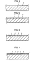
- Figs. 4 to 20 are cross sectional views and perspective views for showing the method.
- a buffer layer 2 made of one nickel oxide, cobalt oxide, magnesium oxide, and titanium is formed on the substrate 1 by a metal-organic chemical vapor deposition (MOCVD) method (Step 301 in Fig. 3).
- MOCVD metal-organic chemical vapor deposition
- the buffer layer 2 of nickel oxide may be formed with gas of sublimated nickel acetyl acetonate.
- the buffer layer 2 of titanium may be formed by sputtering.
- a lower electrode layer 3 of platinum is formed on the buffer layer 2 by sputtering or vacuum vapor deposition, as shown in Fig. 5 (Step 302 in Fig. 3).
- a piezoelectric layer 4 of piezoelectric material such as lead zirconium titanate (PZT) is formed on the lower electrode layer 3 by sputtering or vacuum vapor deposition, as shown in Fig. 6 (Step 303 in Fig. 3).
- PZT lead zirconium titanate
- an upper electrode layer 5 of gold is formed on the piezoelectric layer 4 by sputtering or vacuum vapor deposition (Step 304 in Fig. 3).
- a layer of titanium or chrome may be provided between the piezoelectric layer 4 of PZT and the upper electrode layer 5 of gold. Since titanium and chrome are adhesive to the PZT layer and have affinity with gold to develop a diffusion layer, the layer increases a bonding strength between the piezoelectric layer 4 and the upper electrode layer 5. According to an experiment conducted by applicants, the titanium layer having a thickness ranging from 20 to 100 angstroms increases the bonding strength satisfactorily.
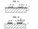
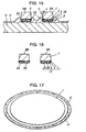
- Figs. 8 to 16 are cross sectional views of the arms 10A and 10B of the sensor.
- a resist film 7 of photosensitive resin material for patterning the element is provided by a photolithography method for patterning the oscillator electrode 5A and the detector electrode 5B of the upper electrode 5 (Step 305 in Fig. 3).
- portions of the upper electrode layer 5 and the piezoelectric layer 4 which are not covered with the resist film 7 are removed by dry-etching to provide the oscillator electrode 5A and the detector electrode 5B (Step 306 in Fig. 3).
- the dry-etching terminates just before reaching the bottom of the piezoelectric layer 4 for preventing an interface between the lower electrode layer 3 and the piezoelectric layer 4 from being assaulted by remover solvent used for removing the resist film 7 in the succeeding process.
- the resist film 7 is removed with organic or alkali remover solvent or by oxygen ashing (Step 307 in Fig. 3).
- the upper electrode 5 is separated into the oscillator electrode 5A and the detector electrode 5B.
- a resist mask 8 is provided similarly to the resist film 7 for covering the oscillator electrode 5A, the detector electrode 5B, and regions of the piezoelectric layer 4 neighboring the electrodes (Step 308 in Fig. 3).
- portions of the piezoelectric layer 4, the lower electrode 3, and the buffer layer 2 which are not covered with the resist mask 8 are dry-etched (Step 309 in Fig. 3).
- the resist mask 8 is provided around each electronic element 13 and is spaced from other resist masks 8 around neighbor electronic elements 13, thus allowing the electronic elements 13 to be isolated from each other.
- the substrate 1 is dry-etched with plural types of gas.
- the types of gas are different from each other in etching condition.
- a first gas of SF 6 for facilitating the etching and a second gas of C 4 F 8 for suppressing the etching are used.
- the substrate 1 is etched with mixture of the two types of gas or with each type of gas alternately.
- the mixture of the types of the gas controls facilitating and suppressing the etching by changing the ratio of the types of gas during the etching, thus controlling an amount of the etching of the substrate 1.
- the ratio appropriately determined allows the substrate 1 to be etched in a direction perpendicular to a surface of the substrate, thus allowing a recess 9 to have side walls and a bottom substantially perpendicular to the side walls.
- the ratio of the first gas is increased, the bottom and each side wall of the recess 9 in the substrate 1 can form an acute angle between the bottom and each side wall of the recess 9.
- the shape of the etched recess 9 in the substrate 1 can favorably be adjusted by controlling the ratio of respective durations of the usage of the types of gas.
- the substrate 1 is etched up to a depth greater than a necessary thickness D1 of the substrate 1. As shown in Fig. 13, the substrate 1 has a cross section of a trapezoidal shape. In the cross section, a width far from a surface where the lower electrode layer 3, the piezoelectric layer 4, and the upper electrode layer 5 are provided is smaller than a side where the electrodes are provided.
- the substrate 1 is bonded to a dummy substrate 11 by an adhesive layer 12 while having the resist mask 8, as shown in Fig. 14 (Step 310 in Fig. 3).
- the resist mask 8 may be removed before the bonding of the substrate.
- the adhesive layer 12 covers at least the upper surface and the side surface of the electronic element 13.
- the adhesive layer 12 is applied abundantly enough to enter into the recess 9 between the arms 10A and 10B of the tuning fork.
- the adhesive layer 12 accordingly holds the arms 10A and 10B securely upon being cured, and thus, increases bonding strength as shown in Fig. 14. Displacement of the sensor against the dummy substrate 11 is accordingly avoided during the substrate 1 is ground, and thus, the substrate 1 I ground uniformly.
- Fig. 14 illustrates the single electronic element. However the dummy substrate 11 is bonded to plural electronic elements with the substrate 1 by the adhesive layer 12.
- the dummy substrate 11 has a planer surface and a physical strength enough to stand a certain mechanical stress caused by removing the substrate 1.
- the dummy substrate 11 may be made of glass, silicon, or SUS material.
- a portion of the substrate 1 is ground off from a back surface of the substrate 1, as shown in Fig. 15 (Step 311 in Fig. 3).
- the grinding can control the thickness of the substrate 1 precisely. More specifically, the substrate 1 is grounded off up to a depth larger than the necessary thickness, as shown in Fig. 13.
- the grinding permits the etching process of the upper electrode layer 5, the piezoelectric layer 4, the lower electrode layer 3, the buffer layer 2, and the substrate 1 while the substrate 1 is thick as being stressed by external force during the production. Accordingly, since the substrate 1 is protected from breakage, the sensor can be manufactured efficiently.
- the substrate 1 is ground off to have the necessary depth after the recess 9 communicates with another recess.
- the electronic elements 13 have the upper and side surfaces secured with the dummy substrate 11 by the adhesive layer 12. Accordingly, as shown in Fig. 18, the electronic elements 13 are held together after the substrate 1 is ground off to be separated into chips.
- the substrate 1 has the cross section of the trapezoidal shape having a ground side narrower than a side opposite to the ground side. This shape protects the substrate 1 from being chipped off at a corner (the portion "a" in Fig. 15) between the top surface and the side wall at the recess 9 even when the substrate is ground after the recess 9 communicates with another recess.
- the trapezoidal cress section of the substrate 1 may be etched as shown in Fig. 19 if the shape influences a frequency response of the sensor.
- the substrate 1 is etched downward, i.e., perpendicularly to the top surface of the substrate.
- an etching condition is changed for having the substrate etched towards the side wall of the substrate (the portion "a” in Fig. 19).
- the etching of the substrate 1 protects the substrate 1 from being chipped off at the comer (the portion "a" in Fig.
- the substrate 1 may be etched towards the side wall with etching gas of xenon difluoride.
- the gas allows the recess 9 to be widened at the bottom as shown in the portion "a" in Fig. 19.
- the side walls of the substrate 1 are protected with a protective coating developed by the preceding etching with the first and second gases. Since the bottom of the substrate 1 is not covered with the protective coating, the bottom can further be etched with the etching gas of xenon difluoride.
- the dummy substrate 11 is removed (Step 312 in Fig. 3), and the resist mask 8 is removed similarly to the resist film 7 (Step 313 in Fig. 3), thus providing an angular rate sensor 15.
- a remaining portion of the adhesive layer 12 may be removed from the electronic element 13. Since the resist mask 8 is isolated from other electronic element 13, the electronic element 13 is connected to adjacent electronic devices 13 only through the adhesive layer 12 and the dummy substrate 11. This arrangement allows the electronic elements 13 to be separated from each other by just removing the adhesive layer 12.
- the upper electrode layer 5 consisting of the oscillator electrode 5A and the detector electrode 5B is covered with the resist mask 8 before the separation of the electronic elements 13, thus being protected from injury and pollution.
- the angular rate sensor is accommodated in a case 14 according to requirement (Step 314 in Fig. 3).
- the electronic device of Embodiment 1 is not limited to the angular rate sensor but may be any other device, such as a chip resistor, a chip oscillator, and a chip actuator, with equal effects.
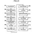
- Fig. 21 is a flowchart for showing a method of manufacturing an angular rate sensor according to Exemplary Embodiment 2 of the present invention.
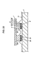
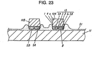
- Figs. 22 to 29 are cross sectional views and perspective views of the sensor for showing processes in the method.
- the senor is manufactured by Steps 301 to 309 of Embodiment 1 shown in Fig. 3 until a substrate 1 is to be dry-etched, as shown in Fig. 21 (Step 309).
- the substrate 1 having the resist mask 8 attached to the substrate is bonded to the dummy substrate 11 by an adhesive layer 51 made of thermoplastic resin, such as paraffin wax used in candles (Step 2110 in Fig. 21).
- the resist mask 8 may be removed before this process.
- An amount of adhesive for forming the adhesive layer 51 may be determined similarly to that of Embodiment 1.
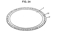
- Fig. 23 illustrates the single electronic element. As shown in Fig. 24, in practice, a surface of the substrate 1 where the electronic elements are provided faces the dummy substrate 11 and is bonded to the dummy substrate 11 by the adhesive layer 51.
- a portion of the substrate 1 is removed similarly to Step 311 in Fig. 3 of Embodiment 1 (Step 2111 in Fig. 21).
- the electronic element 13 is then heated and picked off from the adhesive layer 51 (Step 2112 in Fig. 21). As the thermoplastic resin is softened by the heating of the electronic device 13, the adhesive layer 51 allows the electronic element 13 to be separated easily.
- a heating iron 21 is used for heating the electronic element 13, as shown in Fig. 26.
- a distal end 22 of the heating iron 21 may preferably have a shape identical to or slightly smaller than the shape of the electronic element 13, as shown in Fig. 27. Since a target electronic element 13 is joined to adjacent electronic elements 13 only by the adhesive layer 51 of the thermoplastic resin, heat from the iron 21 can hardly transmitted to other elements.
- the adhesive layer 51 is softened by the heating of the target electronic element 13 adhered to the dummy substrate 11, as shown in Fig. 28, hence allowing the electronic element' 13 to be easily picked off.
- the element may be heated by infrared ray instead of the heating iron 15, as shown in Fig. 29.
- a mask 17 is provided between an infrared-ray source 16 and the dummy substrate 11 in order to allow only the target element 13 to be irradiated with the infrared ray.
- the infrared ray heats and softens the adhesive layer 51 around the target electronic element 13 to allow the element to be picked off easily.
- the target electronic element 13 is adhered to the dummy substrate 11 by the adhesive layer 51 even after the substrate 1 is ground. Therefore, the target electronic device 13 is picked off from the dummy substrate 11 without disturbing the adjacent electronic elements 13, thus preventing the elements from jumble arrangement.
- the resist mask 8 is removed by organic agent or alkali solution, as shown in Fig. 16 (Step 2113 in Fig. 21). At this moment, if necessary, a remaining portion of the adhesive layer 51 may be cleaned up on the electronic device 13.
- the electronic element 13, i.e., the angular rate sensor 21 is accommodated in a case 14, as shown in Fig. 20 (Step 2114 in Fig. 21).
- the electronic device of Embodiment 2 is not limited to the angular rate sensor but may be other device, such as a chip resistor, a chip oscillator, and a chip actuator, with the same effect as that of this embodiment.
- a method of manufacturing an angular rate sensor according to Exemplary Embodiment 3 of the present invention will be described with referring to Figs. 30 to 32.
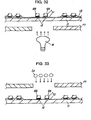
- a layer 18 made of material, such as carbon, for absorbing infrared ray is provided on a dummy substrate 11 differently from Embodiment 2.
- the layer 18 for absorbing infrared ray provided between the adhesive layer 51 and the dummy substrate 11 can be heated rapidly up to a high temperature upon absorbing the infrared ray, thus allowing a target electronic device 13 to be picked off efficiently.
- the dummy substrate 11 upon being made of silicon or glass transmitting the infrared ray, allows the infrared ray to be irradiated from the back surface of the substrate 11 to a desired location of the adhesive layer 51 which holds the electronic device 13, as shown in Fig. 32. This can facilitate the picking of the electronic device 13.
- Other arrangements and materials are identical to those of Embodiment 1.
- an adhesive layer 52 is made of resin for decreasing an adhesive strength of the layer 52 when exposed to ultraviolet ray.
- the resin is used as adhesive agent for a dicing tape.
- the element 13 Before an electronic element 13 is picked off similarly to Embodiment 2, the element 13 is exposed to ultraviolet ray for decreasing an adhesive strength of a portion of the adhesive layer 52 around the element 13, thus allowing the electronic element 13 to be picked off easily.
- a mask 17, similarly to Embodiment 3, may be provided between an ultraviolet ray source 20 and the electronic element 13 for allowing ultraviolet ray to be irradiated only on a target electronic element 13, as shown in Fig. 33.
- the substrate 1 is made of material which does not transmit ultraviolet ray, such as silicon
- the dummy substrate 11 may be made of material transmitting ultraviolet ray, such as silica and borosilicate glass.
- the substrates allow the adhesive layer 52 provided between the electronic device 13 and the dummy substrate 11 to be effectively irradiated at a necessary location with ultraviolet ray from the back surface of the dummy substrate 11, as shown in Fig. 34. Accordingly, the electronic element 13 can be picked off easily.
- Embodiment 1 for manufacturing an angular rate sensor.
- the adhesive layer according to Embodiments 2 to 4 are made of the materials which can be softened by infrared ray or ultraviolet ray. If the adhesive layer is made of material softened by physical operation, the electronic element 13 can be picked off by the operation instead of the infrared ray and the ultraviolet ray with effects identical to that of Embodiments 2 to 4. For example, the adhesive layer may be exposed to electromagnetic waves from an electronic oven.
- the dry etching may be replaced by wet etching or any other appropriate technique for providing the recess 9 in the substrate 1 to pattern a desired electronic element.
- a method of manufacturing an electronic device In a method of manufacturing an electronic device according to the present invention, plural elements are separated at once by removing a portion of a substrate from a surface opposite to a surface having the elements provided thereon. The method allows the devices which include the elements, respectively, to be manufactured efficiently.
Landscapes
- Physics & Mathematics (AREA)
- Engineering & Computer Science (AREA)
- General Physics & Mathematics (AREA)
- Radar, Positioning & Navigation (AREA)
- Remote Sensing (AREA)
- Gyroscopes (AREA)
- Dicing (AREA)
- Manufacturing Of Printed Circuit Boards (AREA)
Abstract
Description
Claims (30)
- A method of manufacturing an electronic device, comprising:forming an element on a front surface of a substrate;providing a recess in the front surface of the substrate around the element; andremoving a portion of the substrate from a back surface of the substrate until reaching the recess.
- The method according to claim 1,
wherein said providing of the recess includes
providing a resist mask on the front surface of the substrate to be provided with the recess, and
etching the front surface of the substrate through the resist mask,
said method further comprising
removing the resist mask. - The method according to claim 2, wherein said removing of the resist mask is executed after said removing of the portion of the substrate.
- The method according to claim 2, wherein said etching of the front surface of the substrate includes dry-etching the front surface.
- The method according to claim 4, wherein said dry-etching of the front surface includes dry-etching the front surface by using first gas and second gas.
- The method according to claim 5, wherein the first gas contains gas for facilitating dry-etching, and the second gas contains gas for suppressing dry-etching.
- The method according to claim 6, wherein said dry-etching of the front surface includes dry-etching the front surface by mixture gas including the first gas and the second gas.
- The method according to claim 7, wherein said dry-etching of the front surface by the mixture gas includes increasing a rate of the first gas in the mixture gas according to proceeding said providing of the recess in the front surface of the substrate.
- The method according to claim 6, wherein said dry-etching of the front surface includes dry-etching the front surface by using the first gas and the second gas alternately.
- The method according to claim 9, wherein said dry-etching of the front surface by using the first gas and the second gas alternately includes increasing a duration when the recess is provided by the first gas according to proceeding said providing of the recess in the front surface of the substrate.
- The method according to claim 4, further comprising
dry-etching the substrate by xenon difluoride. - The method according to claim 1, further comprising
bonding a dummy substrate to the front surface of the substrate through an adhesive layer. - The method according to claim 12, wherein the adhesive layer is provided on a surface of the element and around the element.
- The method according to claim 1, further comprising
picking off the element. - The method according to claim 14, further comprising
mounting the element on a member. - The method according to claim 14, further comprising
bonding a dummy substrate to the front surface of the substrate by an adhesive layer. - The method according to claim 16, wherein the adhesive layer is provided on a surface of the element and around the element.
- The method according to claim 16, wherein the adhesive layer comprises thermoplastic resin.
- The method according to claim 18, wherein the adhesive layer is made of the thermoplastic resin.
- The method according to claim 18, further comprising
heating the element. - The method according to claim 20, wherein said heating of the element includes heating the element with a heating iron.
- The method according to claim 20, wherein said heating of the element includes allowing the element to be irradiated with infrared ray.
- The method according to claim 22, wherein a layer capable of absorbing infrared ray is provided between the dummy substrate and the adhesive layer.
- The method according to claim 22, wherein the dummy substrate comprises silicon.
- The method according to claim 22, wherein the dummy substrate comprises glass material which can transmit infrared ray.
- The method according to claim 16, wherein the adhesive layer comprises resin material having adhesive strength decreased by ultraviolet ray.
- The method according to claim 26, further comprising
irradiating the adhesive layer with ultraviolet ray. - The method according to claim 26, wherein the dummy substrate comprises material capable of transmitting ultraviolet ray.
- The method according to claim 1,
wherein the element is one of a plurality of elements, and
wherein said providing of the recess includes providing the recess between the plurality of elements. - The method according to claim 29, further comprising
exposing at least one of the plurality of elements through a mask.
Applications Claiming Priority (5)
| Application Number | Priority Date | Filing Date | Title |
|---|---|---|---|
| JP2002016553 | 2002-01-25 | ||
| JP2002016553A JP4259019B2 (en) | 2002-01-25 | 2002-01-25 | Manufacturing method of electronic parts |
| JP2002043018 | 2002-02-20 | ||
| JP2002043018A JP2003243330A (en) | 2002-02-20 | 2002-02-20 | Manufacturing method of electronic components |
| PCT/JP2003/000637 WO2003063219A1 (en) | 2002-01-25 | 2003-01-24 | Method for manufacturing electronic component |
Publications (2)
| Publication Number | Publication Date |
|---|---|
| EP1388890A1 true EP1388890A1 (en) | 2004-02-11 |
| EP1388890A4 EP1388890A4 (en) | 2007-10-31 |
Family
ID=27615696
Family Applications (1)
| Application Number | Title | Priority Date | Filing Date |
|---|---|---|---|
| EP03703043A Withdrawn EP1388890A4 (en) | 2002-01-25 | 2003-01-24 | METHOD FOR MANUFACTURING AN ELECTRONIC COMPONENT |
Country Status (4)
| Country | Link |
|---|---|
| US (1) | US6984572B2 (en) |
| EP (1) | EP1388890A4 (en) |
| CN (1) | CN1271684C (en) |
| WO (1) | WO2003063219A1 (en) |
Families Citing this family (11)
| Publication number | Priority date | Publication date | Assignee | Title |
|---|---|---|---|---|
| JP4434537B2 (en) * | 2001-08-27 | 2010-03-17 | パナソニック株式会社 | Piezoelectric functional parts |
| JP4631329B2 (en) * | 2004-07-01 | 2011-02-16 | パナソニック株式会社 | Angular velocity sensor and manufacturing method thereof |
| JP4404218B2 (en) * | 2006-03-29 | 2010-01-27 | セイコーエプソン株式会社 | Tuning fork vibrator and manufacturing method thereof |
| TWI398097B (en) * | 2009-11-18 | 2013-06-01 | Wafer Mems Co Ltd | Tuning fork quartz crystal resonator |
| US9343651B2 (en) * | 2010-06-04 | 2016-05-17 | Industrial Technology Research Institute | Organic packaging carrier |
| US10141906B1 (en) | 2010-06-15 | 2018-11-27 | Hrl Laboratories, Llc | High Q quartz-based MEMS resonators and method of fabricating same |
| US9985198B1 (en) | 2010-06-15 | 2018-05-29 | Hrl Laboratories, Llc | High Q quartz-based MEMS resonators and methods of fabricating same |
| US8765615B1 (en) * | 2010-06-15 | 2014-07-01 | Hrl Laboratories, Llc | Quartz-based MEMS resonators and methods of fabricating same |
| JP2013178179A (en) * | 2012-02-28 | 2013-09-09 | Seiko Epson Corp | Sensor element, sensor device, and electronic apparatus |
| KR101356933B1 (en) * | 2012-12-28 | 2014-01-29 | 고려대학교 산학협력단 | Apparatus and method for separating micro-nano scale particles using surface acoustic wave-based microfluidic chromatography |
| US10110198B1 (en) | 2015-12-17 | 2018-10-23 | Hrl Laboratories, Llc | Integrated quartz MEMS tuning fork resonator/oscillator |
Family Cites Families (20)
| Publication number | Priority date | Publication date | Assignee | Title |
|---|---|---|---|---|
| JPS5346270A (en) * | 1976-10-08 | 1978-04-25 | Nec Corp | Production of semiconductor device |
| JPH0626208B2 (en) | 1985-02-14 | 1994-04-06 | 株式会社東芝 | Dry etching method |
| JP2687573B2 (en) * | 1989-04-14 | 1997-12-08 | 富士通株式会社 | Method for manufacturing semiconductor device |
| JP3303379B2 (en) * | 1992-12-09 | 2002-07-22 | 株式会社村田製作所 | Angular velocity sensor |
| JPH06208976A (en) * | 1993-01-08 | 1994-07-26 | Sumitomo Electric Ind Ltd | Method of manufacturing semiconductor device and method of forming through hole |
| JPH0722358A (en) * | 1993-06-15 | 1995-01-24 | Sharp Corp | Method for manufacturing semiconductor device |
| JPH097973A (en) * | 1995-06-16 | 1997-01-10 | Nec Kansai Ltd | Apparatus for manufacturing semiconductor device |
| JPH1047971A (en) * | 1996-08-05 | 1998-02-20 | Nippon Soken Inc | Angular velocity sensor |
| US6294439B1 (en) * | 1997-07-23 | 2001-09-25 | Kabushiki Kaisha Toshiba | Method of dividing a wafer and method of manufacturing a semiconductor device |
| JPH1167699A (en) | 1997-08-13 | 1999-03-09 | Texas Instr Japan Ltd | Method for manufacturing semiconductor device |
| US5972781A (en) * | 1997-09-30 | 1999-10-26 | Siemens Aktiengesellschaft | Method for producing semiconductor chips |
| JP2001523046A (en) * | 1997-11-11 | 2001-11-20 | アービン・センサーズ・コーポレイション | Method for thinning a semiconductor wafer with circuits and wafer made by the method |
| JP2000306887A (en) * | 1999-04-19 | 2000-11-02 | Matsushita Electronics Industry Corp | Method and apparatus of treating wafer |
| DE19962763C2 (en) * | 1999-07-01 | 2001-07-26 | Fraunhofer Ges Forschung | Wafer dicing method |
| DE60033218T2 (en) * | 1999-07-02 | 2007-11-15 | Canon K.K. | A method of manufacturing a liquid ejection head, liquid ejection head, head cartridge, liquid ejection device, silicon substrate manufacturing method, and silicon plate produced thereby |
| JP2001148358A (en) * | 1999-11-19 | 2001-05-29 | Disco Abrasive Syst Ltd | Semiconductor wafer and method for dividing semiconductor wafer |
| US6425971B1 (en) * | 2000-05-10 | 2002-07-30 | Silverbrook Research Pty Ltd | Method of fabricating devices incorporating microelectromechanical systems using UV curable tapes |
| JP3768069B2 (en) | 2000-05-16 | 2006-04-19 | 信越半導体株式会社 | Thinning method of semiconductor wafer |
| WO2001089987A1 (en) * | 2000-05-23 | 2001-11-29 | Silverbrook Research Pty Ltd | Method of fabricating devices incorporating microelectromechanical systems using at least one uv curable tape |
| JP2002016021A (en) * | 2000-06-28 | 2002-01-18 | Toshiba Corp | Semiconductor chip production method and semiconductor chip |
-
2003
- 2003-01-24 US US10/473,980 patent/US6984572B2/en not_active Expired - Lifetime
- 2003-01-24 WO PCT/JP2003/000637 patent/WO2003063219A1/en not_active Ceased
- 2003-01-24 EP EP03703043A patent/EP1388890A4/en not_active Withdrawn
- 2003-01-24 CN CN03800194.2A patent/CN1271684C/en not_active Expired - Fee Related
Also Published As
| Publication number | Publication date |
|---|---|
| CN1507650A (en) | 2004-06-23 |
| CN1271684C (en) | 2006-08-23 |
| EP1388890A4 (en) | 2007-10-31 |
| US6984572B2 (en) | 2006-01-10 |
| US20040132310A1 (en) | 2004-07-08 |
| WO2003063219A1 (en) | 2003-07-31 |
Similar Documents
| Publication | Publication Date | Title |
|---|---|---|
| US5006202A (en) | Fabricating method for silicon devices using a two step silicon etching process | |
| US6984572B2 (en) | Method for manufacturing electronic component | |
| EP0786345B1 (en) | Ink jet recording head and manufacturing method therefor | |
| US7083740B2 (en) | Method for manufacturing resonant device | |
| US20080297006A1 (en) | Piezoelectric actuator and method of producing the same | |
| JP3460218B2 (en) | Ink jet printer head and method of manufacturing the same | |
| EP1357611B1 (en) | Piezoelectric functional part and method of manufacturing the part | |
| US6433390B1 (en) | Bonded substrate structures and method for fabricating bonded substrate structures | |
| US5352566A (en) | Method of manufacturing optoelectronic components | |
| US8516888B2 (en) | Angular velocity sensor and method of manufacturing the same | |
| US6688731B1 (en) | Piezoelectric thin film element, ink jet recording head using such a piezoelectric thin film element, and their manufacture methods | |
| US8021562B2 (en) | Method for manufacturing a filter substrate, inkjet recording head, and method for manufacturing the inkjet recording head | |
| JP2009226660A (en) | Method for patterning by dry etching, mold used for it and method for manufacturing inkjet head | |
| US9333750B2 (en) | Method of processing substrate | |
| EP3712973B1 (en) | Method for producing oscillator substrate and oscillator substrate | |
| JP5099061B2 (en) | Coating film forming method and piezoelectric element manufacturing method | |
| US6613687B2 (en) | Reverse reactive ion patterning of metal oxide films | |
| US20050051511A1 (en) | Method for manufacturing chemical sensors | |
| JP4259019B2 (en) | Manufacturing method of electronic parts | |
| EP2327115B1 (en) | Removing piezoelectric material using electromagnetic radiation | |
| EP4287507A1 (en) | Crystal oscillator and method of making the same | |
| JP2003243330A (en) | Manufacturing method of electronic components | |
| JP2008061313A (en) | Electrostatic actuator, droplet discharge head, droplet discharge apparatus, electrostatic device, and manufacturing method thereof | |
| JP2004074806A (en) | Ink jet recording head and method of manufacturing the same | |
| CN100548867C (en) | Method for manufacturing suspension structure |
Legal Events
| Date | Code | Title | Description |
|---|---|---|---|
| PUAI | Public reference made under article 153(3) epc to a published international application that has entered the european phase |
Free format text: ORIGINAL CODE: 0009012 |
|
| 17P | Request for examination filed |
Effective date: 20031029 |
|
| AK | Designated contracting states |
Kind code of ref document: A1 Designated state(s): AT BE BG CH CY CZ DE DK EE ES FI FR GB GR HU IE IT LI LU MC NL PT SE SI SK TR |
|
| RIC1 | Information provided on ipc code assigned before grant |
Ipc: H01L 21/304 20060101AFI20070707BHEP |
|
| A4 | Supplementary search report drawn up and despatched |
Effective date: 20071002 |
|
| RAP1 | Party data changed (applicant data changed or rights of an application transferred) |
Owner name: PANASONIC CORPORATION |
|
| 17Q | First examination report despatched |
Effective date: 20090604 |
|
| STAA | Information on the status of an ep patent application or granted ep patent |
Free format text: STATUS: THE APPLICATION IS DEEMED TO BE WITHDRAWN |
|
| 18D | Application deemed to be withdrawn |
Effective date: 20150801 |