EP1388877A1 - Plasma display panel, back and front substrates for plasma display panel, and coated metal particle for forming electrode - Google Patents
Plasma display panel, back and front substrates for plasma display panel, and coated metal particle for forming electrode Download PDFInfo
- Publication number
- EP1388877A1 EP1388877A1 EP02720631A EP02720631A EP1388877A1 EP 1388877 A1 EP1388877 A1 EP 1388877A1 EP 02720631 A EP02720631 A EP 02720631A EP 02720631 A EP02720631 A EP 02720631A EP 1388877 A1 EP1388877 A1 EP 1388877A1
- Authority
- EP
- European Patent Office
- Prior art keywords
- metal particles
- plasma display
- electrode
- coated metal
- display panel
- Prior art date
- Legal status (The legal status is an assumption and is not a legal conclusion. Google has not performed a legal analysis and makes no representation as to the accuracy of the status listed.)
- Withdrawn
Links
Images

Classifications
-
- H—ELECTRICITY
- H01—ELECTRIC ELEMENTS
- H01J—ELECTRIC DISCHARGE TUBES OR DISCHARGE LAMPS
- H01J11/00—Gas-filled discharge tubes with alternating current induction of the discharge, e.g. alternating current plasma display panels [AC-PDP]; Gas-filled discharge tubes without any main electrode inside the vessel; Gas-filled discharge tubes with at least one main electrode outside the vessel
- H01J11/10—AC-PDPs with at least one main electrode being out of contact with the plasma
- H01J11/12—AC-PDPs with at least one main electrode being out of contact with the plasma with main electrodes provided on both sides of the discharge space
-
- H—ELECTRICITY
- H01—ELECTRIC ELEMENTS
- H01J—ELECTRIC DISCHARGE TUBES OR DISCHARGE LAMPS
- H01J11/00—Gas-filled discharge tubes with alternating current induction of the discharge, e.g. alternating current plasma display panels [AC-PDP]; Gas-filled discharge tubes without any main electrode inside the vessel; Gas-filled discharge tubes with at least one main electrode outside the vessel
- H01J11/20—Constructional details
- H01J11/22—Electrodes, e.g. special shape, material or configuration
-
- H—ELECTRICITY
- H01—ELECTRIC ELEMENTS
- H01J—ELECTRIC DISCHARGE TUBES OR DISCHARGE LAMPS
- H01J9/00—Apparatus or processes specially adapted for the manufacture, installation, removal, maintenance of electric discharge tubes, discharge lamps, or parts thereof; Recovery of material from discharge tubes or lamps
- H01J9/02—Manufacture of electrodes or electrode systems
-
- H—ELECTRICITY
- H01—ELECTRIC ELEMENTS
- H01J—ELECTRIC DISCHARGE TUBES OR DISCHARGE LAMPS
- H01J2211/00—Plasma display panels with alternate current induction of the discharge, e.g. AC-PDPs
- H01J2211/20—Constructional details
- H01J2211/22—Electrodes
- H01J2211/225—Material of electrodes
Definitions
- This invention relates to a plasma display panel, front and back substrates, and coated metal particles for electrode formation.
- a need to reduce the volume and thickness of stationary displays has arisen in recent years owing to the increased size of the display plates.
- Various flat panel displays have been developed.
- the plasma display panel PDP
- the plasma display panel is being utilized as an alternative to CRT picture tubes currently used in televisions and in this and other aspects has moved into the realm of practical application.
- Fine metal wiring is required to increase the open area of the front substrate.
- sputtering and patterning steps are used to form the front substrate.
- a film is formed from various metals and metal oxides for electrodes using a vacuum device (sputtering device).
- sputtering device a vacuum device
- an electrode pattern is formed by photolithography.
- metal wiring can be also formed by screen printing. Since fine metal wiring is hard to obtain by this method, the open area of the front substrate is reduced.
- Back substrate formation is subject to the same requirements as those of the front substrate since the same steps are performed.
- Japanese Patent Laid-open Nos. S59(1984)-189617, S59(1984)-202682, S60(1985)-137886 and S60(1985)-160690 teach formation of an electrode pattern from conductive particles by electrophotography followed by sintering.
- Japanese Patent Laid-open No. H10(1998)-041066 teaches a method in which a conductive pattern is formed by electrophotography on a ceramic green sheet using developing agents containing insulative surface-treated metal particles and carrier particles.
- the inventors found that the above problem can be solved by printing an electrode wiring pattern on a base substrate by electrophotography using metal particles coated with thermoplastic resin and thereafter heating the resulting substrate at a certain temperature to decompose and evaporate the thermoplastic resin, thereby making the wiring pattern conductive.
- an object of the present invention is to provide a plasma display panel, and front and back substrates for plasma display panels which can be efficiently manufactured with little waste of materials, and to provide coated metal particles for the formation of electrodes.
- a plasma display panel comprising: a back substrate that has a first metal electrode on a back base substrate, and a front substrate, arranged opposite to the back substrate, that has a transparent electrode and a second metal electrode on a front base substrate, at least one of the first metal electrode and the second metal electrode being formed by electrophotography.
- a back substrate for a plasma display panel comprising a metal electrode formed by electrophotography.
- a front substrate for a plasma display panel comprising a metal electrode formed by electrophotography.
- desired fine wires of, for example, a width of about 10 to about 200 ⁇ m, preferably about 20 to about 100 ⁇ m, and a thickness of about 0.1 to about 2 ⁇ m, can be accurately formed, since the first and second metal electrodes are printed by electrophotography. It is therefore possible to achieve the high precision and narrow pitch required for substrates of plasma display panels.
- electrophotographic printing reduces waste of materials and does not require a large amount of labor.
- printing by electrophotography can be applied in cases where various kinds but small amount of patterns are required.
- the present invention provides coated metal particles for electrode formation comprising: metal particles whose average diameter is 0.1 to 20 ⁇ m, and a thermoplastic resin that coats the metal particles.
- the coating of the metal particle with the thermoplastic resin makes the coated metal particles insulative, thereby enabling use of the insulate particles as toner in electrophotography.
- thermoplastic resin of the coated metal particles for electrode formation is preferably polyethylene type resin.
- the polyethylene type resin can prevent adhesion in a developer and "spent" of carriers.
- thermoplastic resin is preferably polymerized on the metal particle surface.
- Polymerization of the resin on the particle surface enables uniform coating of the particles, and also makes it possible to change the thickness of the coating layer as desired.
- the coated metal particles for electrode formation preferably comprise a metal selected from the group consisting of Sn, Ag, Pb, Bi, Cu, In, Ni, Zn, W, Ta, Mo, Al, Au and Cr, or an alloy of at least two elements selected from among the above group.
- coated metal particles for the formation of electrodes hereinafter referred to as “coated metal particles”
- coated metal particles the plasma display panel made using the particles according to the present invention
- coated metal particles according to the present invention each contains a metal particle and a thermoplastic resin coating the surface of the particle (resin coating layer).
- the metal particles can be made of any conductive material with no limitation on kind.
- Materials for the metal particles include metallic elements selected from the group consisting of Sn, Ag, Pb, Bi, Cu, In, Ni, Zn, W, Ta, Mo, Al, Au and Cr, and alloys of at least two elements selected from among the above group.
- Preferred metals are Sn, Ag, Pb, Cu, W, Ta and Mo, and more preferred metals are Ag and Cu.
- W alloys such as WTa and MoW, Al alloys, solders, and solder-free-alloys.
- Metal particles of any shape such as spherical and irregular can be used without limitation. Spherical, e.g., uniform true spherical, is preferred.
- the diameter of the metal particles is preferably 0.1 to 20 ⁇ m. If the diameter is smaller than 0.1 ⁇ m, the metal particles are liable to agglomerate when coated with thermoplastic resin and, when the particles are used as toner, the toner may scatter at the time of printing to lower the quality of the printed images.
- the diameter exceeds 20 ⁇ m, the particles cannot be readily used as toner. As a result, the quality of print images may be degraded and the electrode wiring may not be formed with high-accuracy.
- the diameter is more preferably 0.2 to 10 ⁇ m, still more preferably 3 to 6 ⁇ m.
- the metal particles preferably account for 80 wt.% or more of the total coated metal particles. If they account for less than 80 wt.%, the coating layer becomes unnecessarily thick. This prevents the metal particles coming into close contact with each other at the time of printing an electrode wiring pattern, in which case sufficient conductivity may not be obtained after removal of the resin by heating. Further, the flowability of the metal particles decreases as the bulk density increases. This deceases the flowability of developing agents obtained by mixing them with carriers. As a result, the stability may be remarkedly lowered at the time of developing.
- the metal particles more preferably account for 90 wt.% or more of the total coated metal particles.
- the resin coating layer can completely cover the surface of the metal particles.
- the resin layer cannot completely cover the surface of the metal particles because the metal particle content is too large, insulating defects disadvantageously occur to degrade the printed images.
- the upper limit changes dependent on properties such as relative density and the geometry of the surface, and the diameter of the metal particles.
- the metal particle content indirectly defines the thickness of the resin coating layer in the coated metal particles of the present invention.
- thermoplastic resins there is no limitation on the kind of the thermoplastic resin.
- Usable thermoplastic resins include acrylic type resins and polyolefin type resins. Polyolefin type resins are preferable. More preferred resins are polyethylene resins that can be produced by direct polymerization on the surface of the metal particles. These thermoplastic resins will discompose and disappear at the sintering step after printing the electrode wiring, thereby imparting conductivity to the electrode wiring.
- a polyolefin type resin is used as a thermoplastic resin
- monomers are preferably polymerized directly on the surface of the metal particles to produce a resin layer made of a high-molecular polyolefin.
- the high-molecular polyolefin preferably has a number average molecular weight of 2,000 or more or a weight average molecular weight of 10,000 or more.
- the high-molecular polyolefin is different from polyethylene wax which are known as low-molecular polyethylenes, e.g., Mitsui high wax (Mitsui Chemicals, Inc.), San wax (Sanyo Chemical Co., Ltd.), Polyrez (neutral wax; Polymer Co., Ltd.), Dialene 30 (Mitsubishi Chemical Industries, Ltd.), Nisseki Lexpole (Nippon Oil Co.), Neowax (Yasuhara Chemical Co., Ltd.), AC polyethylene (Allied Chemical Inc.), Eporene (Eastman Kodak Company), Hoechst wax (Hoechst Inc.), A-Wax (BASF Ltd.), Polywax (Petrolite Inc.), Escomer (Exxon Chemical Co.) and the like.
- Mitsui high wax Mitsubishi Chemicals, Inc.
- San wax San wax
- Polyrez Polyrez
- Dialene 30 Mitsubishi Chemical Industries, Ltd.
- Nisseki Lexpole Nippon Oil Co.
- Neowax Y
- Polyethylene wax can be dissolved in heated toluene or the like and applied to the metal particles by means of an ordinary dipping or spray method.
- the polyethylene layers may peel from the surfaces of the metal particles owing to, for example, shearing forces arising in the developing device at the time of printing, since the mechanical strength of the resin is low.
- a polyolefin layer formed of polyethylene wax is not suitable for use in the present invention.
- the metal particle surface is treated with a catalyst for olefin polymerization and olefin monomers are polymerized directly on the treated surface to form a resin coating layer.
- Japanese Patent Laid-open Nos. S60(1985)-106808 and S60(1985)-106810 teach a polymerization method. Specifically, metal particles are pre-treated with a high activity catalyst component that contains titanium and/or zirconium and can be dissolved in a hydrocarbon solvent such as hexane or heptane. The pre-treated product and an organic aluminum compound are suspended in a hydrocarbon solvent. Olefin monomers are supplied to the suspension to be polymerized directly on the surfaces of the metal particles.
- coatings obtained by the direct formation on the surfaces of metal particles have excellent strength.
- the direct formation can produce uniform coating layers, and any desired film thickness can be obtained by changing the amount of olefin.
- the coated metal particles of the present invention can be subjected to flattening.
- the printing of the so-processed particles makes it possible to obtain wiring in which the particles contact each other more closely.
- the flattening method used can be optimally selected from among the following.
- Coated metal particles are treated for several tens of minutes at in a mixer such as a Henschel mixer (Mitsui Mining Co., Ltd.) and Mechano mill (Okada Seiko Co., Ltd.)at a low rotation speed that does not deform the particles. Flattened coated metal particles can be obtained as a result.
- a mixer such as a Henschel mixer (Mitsui Mining Co., Ltd.) and Mechano mill (Okada Seiko Co., Ltd.)at a low rotation speed that does not deform the particles.
- Flattened coated metal particles can be obtained as a result.
- Coated metal particles are dispersed in an air flow by, e.g., using a thermal sphericallization machine (Hosokawa Micron Co.)
- the dispersed particles are rapidly heated to a temperature above the melting point of polyethylene and then rapidly cooled to be flattened without aggregation.
- Coated metal particles are flattened by being brought into collision with each other or a rotary blade using, e.g., a jet mill (counter jet mill, Hosokawa Micron Co.) and a hybridizer (hybridization, Nara Kikai Seisakusho).
- a jet mill counter jet mill, Hosokawa Micron Co.
- a hybridizer hybridization, Nara Kikai Seisakusho
- Coated metal particles produced by direct polymerization form very weak aggregates which can be broken between the fingers at the time of filtering and drying.
- the aggregates can be broken up by subjecting them to oscillating sieving using a screen of 125 ⁇ m or less mesh in addition to the above flattening.
- They may be also broken up by any method of applying shear stress to the particles such as by using a ribbon mixer or a Nauta mixer.
- the coated metal particles are required to have a prescribed amount of charge to form developing agents and print electrode wiring by electrophotography.
- the metal particles are completely coated.
- An increase in the amount of the coating thermoplastic resin increases the insulating property of the coated metal particles.
- the resistance value of the coated metal particles produced by the above method is too low to be measured by an ordinary powder resistance measuring method.
- a layer of the coated metal particles with a thickness of 0.5 cm is formed between upper and lower electrodes in an electrode area of 5 cm 2 under a load of 1 kg.
- a voltage of 1 to 500 V is applied across the electrodes and the current passing through the bottom is measured to calculate the resistance.
- electrode wiring is printed by electrophotography and the wiring is thereafter baked to decompose and sinter the thermoplastic resin to form a substrate for a plasma display.
- This requires close contact of the coated metal particles.
- the coating resin on the surface of the coated metal particles functions as a binder and becomes fixed.
- a suitable amount of resin is required, which amount changes depending on particle diameter and the like.
- the bulk density of the coated metal particles of the present invention is about 1.0 to about 8.5 g/cc but changes dependent on the particle diameter and type of metal.
- the above-mentioned flattening treatment increases the bulk density.
- the bulk density is closely related to flowability. If the bulk density increases, the flowability of developing agents using the coated metal particles increases in proportion.
- Electrode wiring can be printed in any of a 1, 1.5 or 2 component system.
- the 2 component system is preferred where the toner is mixed with carriers to form a developing agent.
- Preferred carriers include magnetic powder such as ferrite, magnetite and iron powder; resin coated carriers obtained by coating carriers with resin; binder type carriers obtained by adding magnetic powder to resin; and polymerized coated carriers obtained by effecting polymerization directly on the surfaces of magnetic powder.
- the coated metal particles of the present invention have five to ten times higher density than that of toners generally used in copying machines and printers.
- the ratio of general toners to carriers is 2 to 40 wt.%.
- the coated metal particles are required to be mixed with carriers in a ratio of 10 to 400 wt.%.
- the developing agent In order to print electrode wiring with the coated metal particles of the present invention, the developing agent must be prepared in the above way.
- the printing machine Any machine capable of forming images by electrophotography, e.g., ONDEMAND printers as well as commercially available printers and copying machines, can be used.
- the polarity of the toner required changes between positive charge and negative charge dependent on whether the machine uses an amorphous silicon body system or an organic photosensitive body system. The required polarity can be imparted by properly selecting the specifications of the carriers or the type of charging roller.
- a machine must be modified, for example, to form space for receiving base substrates corresponding to the thickness thereof at the time of transfer. Additionally, the transfer system for base substrates must be one that does not soil the surfaces of the substrates or distort the substrates.
- Any printing among the 1, 1.5 or 2 component systems can be used so far as it uses the electrophotographic technique.
- the computer When, similarly to the case of using a printer, the printing data are supplied by a computer, the computer is first used to create the wiring diagram and printing is then conducted for the required number of copies. Identical metal wiring can be always obtained in this way. Unlike production of screens using a photoresist or screen printing process, which involves considerable expense, this way is free of problems such as the high cost and low stability encountered by the photoresist method.
- the address electrodes and upper metal electrodes are printed by electrophotography. Parts other than the electrodes can be formed from ordinary materials by ordinary methods without any particular limitation. [Embodiment 1]
- Fig. 1 is a sectional view showing one embodiment of the plasma display panel of the present invention.
- a plasma display panel 1 is made of a back substrate 10 and a front substrate 20.
- the back substrate 10 comprises a back glass substrate (back base substrate) 12, a metal address electrode (first electrode) 14, a barrier wall 16 and a fluorophor 18.
- the front substrate 20 comprises a front glass substrate (front base substrate) 22, a transparent electrode 24, an upper metal electrode (second electrode) 26, a dielectric layer 28 and a protective layer 30.
- the metal address electrode 14 is printed on the back glass substrate 12 by electrophotography as explained later. Thereafter the back glass substrate 12 with the metal address electrode 14 formed thereon is heated to 500 to 600°C to decompose and remove the resin coating, thereby sintering the metal electrode.
- the transparent electrode 24 is formed on the front glass substrate 22.
- the upper metal electrode 26 is then printed on the substrate 22 by electrophotography as explained later.
- the resulting substrate 22 is similarly heated to 500 to 600°C.
- the barrier wall 16 is formed on the back glass substrate 12 and the fluorophor 18 is disposed to produce the back substrate 10.
- the dielectric layer 28 and protective layer 30 are laminated on the front glass substrate 22 in this order to produce the front substrate 20. These substrates 10, 20 are adhered to each other to form the plasma display panel 1.
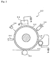
- FIG. 2 is a diagrammatic view of an electrophotography apparatus 50 for the formation of the metal address electrode 14 and upper metal electrode 26 using coated metal particles.
- This apparatus 50 is an ordinary electrophotography apparatus in which a charging unit 54, an image signal exposure unit 56, a developing unit 58, a transfer roll 60, a cleaning blade 64 and a whole image exposure unit 66 are arranged around a photosensitive drum 52.
- a substrate 62 is provided between the photosensitive drum 52 and the transfer roll 60.
- the charging unit 54 and image signal exposure unit 56 form an electrostatic latent image on the rotating drum 52.
- the developing unit 58 supplies coated metal particles to form an electrode wiring image corresponding to the latent image.
- the transfer roll 60 then transfers the electrode wiring image to the surface of the substrate 62 (back glass substrate 12 or front glass substrate 22).
- the substrate 62 is heated to temporarily fix the electrode wiring.
- the substrate 62 is further heated and sintered so that the thermoplastic resin decomposes and the metal particles are sintered.
- the coated metal particles that were not transferred to the substrate 62 are removed by the cleaning blade 64.
- coated metal particles were produced using the catalyst prepared in Reference Example 1.
- the reaction system was heated to 90°C and ethylene was continuously supplied so as to maintain the system internal pressure at 4.3 kg/cm 2 G until the total amount of ethylene, 13.2 g, was introduced.
- Polymerization for 10 minutes yielded 263.2 g of polyethylene coated Ag particles.
- the dried particles were uniformly gray. Observation under an electron microscope showed that the surfaces of the Ag particles were coated with a thin polyethylene layer.
- Measurement of the composite particles with a TGA (thermobalance) revealed that Ag particles:polyehtylene was 95:5.
- the composite particles were filtered, dried, and treated with an oscillating sieve of 53 ⁇ m mesh to produce coated metal particles A.
- Coated metal particles B were obtained in a similar way to Example 1 except for substituting Cu particles (manufactured by Dowa Kogyo Co., 3 ⁇ m) for the Ag particles.
- Coated metal particles C were obtained in a similar way to Example 2 except for changing the diameter of the Cu particles from 3 ⁇ m to 6 ⁇ m.
- Coated metal particles D were obtained in a similar way to Example 1 except for substituting In/Ag alloy particles (manufactured by Sinku Chikin Co., 2 ⁇ m) for the Ag particles.
- the coated metal particles A were heated at 200°C with a thermal sphere machine (Hosokawa Micron Co.) and rapidly cooled, thereby obtaining flattened coated metal particles E.
- a thermal sphere machine Hosokawa Micron Co.
- the coated metal particles A were treated by a hybridizer (Nara Kikai Kogyo Co., hybridization system) at 12,000 rpm for ten minutes, thereby obtaining flattened coated metal particles F.
- a hybridizer NaKikai Kogyo Co., hybridization system
- Coated metal particles H were obtained in a similar way to Example 7 except for using phenol resin (Asahi Yukizai Co.) and methyl alcohol as the resin and solvent.
- Coated metal particles I were obtained in a similar way to Example 2 except for changing the diameter of the Cu particles from 3 ⁇ m to 25 ⁇ m.
- the coated metal particles A to I were mixed with resin-coated carriers at a weight ratio of 20:100. Hydrophobic silica was added at an amount of 0.7 wt.% of the weight of the coated metal particles and mixed to obtain developing agents. In a commercially available printer (FS600, Kyocera Co.), developing agents set therein were replaced with the agents obtained. Printing was then carried out on various substrates made of paper, PET film, glass and polyimide and evaluated for background fog, density, fixing stability and clearness of fine lines. For the evaluation of background fog, the densities of white (non-printed) part and printed part on a printing surface were measured using a Macbeth illuminometer.
- the coated metal particles A to I were mixed with resin coated carriers at a weight ratio of 20:100. To the mixture was further added and mixed 0.7 wt.% of hydrophobic silica relative to the weight of the coated metal particles, thereby preparing developing agents. In a commercially available printer (FS600, Kyocera Co.), developing agents set therein were replaced with the agents obtained. Fine wires with a width of 100 ⁇ m were then printed on a glass. The glass with the fine wiring thereon was temporarily fixed at 180°C and sintered at 600°C. Conductivity was confirmed. Metal Particle A B C D E F G H I Resistance ⁇ ⁇ ⁇ ⁇ ⁇ ⁇
- the present invention provides a plasma display panel, and front and back substrates for plasma display panels, that can be efficiently manufactured with little waste of materials, and also provides coated metal particles for the formation of electrodes.
Landscapes
- Engineering & Computer Science (AREA)
- Physics & Mathematics (AREA)
- Plasma & Fusion (AREA)
- Manufacturing & Machinery (AREA)
- Chemical & Material Sciences (AREA)
- Materials Engineering (AREA)
- Developing Agents For Electrophotography (AREA)
- Gas-Filled Discharge Tubes (AREA)
Abstract
In a plasma display panel, a back substrate has a
first metal electrode on a back base substrate, and a front
substrate has a transparent electrode and a second metal
electrode on a front base substrate. The front substrate is
arranged opposite to the back substrate. At least one of
the first metal electrode and the second metal electrode
being formed by e electrophotographic printing. At this
time, coated metal particles are used as toner, which
particles are formed by coating metal particles having an
average diameter of 0.1 to 20 µm with thermoplastic resin.
The electrophotographic printing enables manufacture of
plasma display panels and the like with less waste of
materials.
Description
This invention relates to a plasma display panel,
front and back substrates, and coated metal particles for
electrode formation.
A need to reduce the volume and thickness of
stationary displays has arisen in recent years owing to the
increased size of the display plates. Various flat panel
displays (thin-type displays) have been developed. Among
these flat panel displays, the plasma display panel (PDP)
achieves flat display on a large screen, light weight and
reduced thickness, as well as a wide angle of visibility
that enables the user to view the screen from almost totally
sidewise angles. The plasma display panel is being utilized
as an alternative to CRT picture tubes currently used in
televisions and in this and other aspects has moved into the
realm of practical application.
Fine metal wiring is required to increase the open
area of the front substrate. Thus, in a conventional method
of manufacturing a plasma display panel, sputtering and
patterning steps are used to form the front substrate. In
the sputtering step, a film is formed from various metals
and metal oxides for electrodes using a vacuum device
(sputtering device). In the patterning step, an electrode
pattern is formed by photolithography.
However, these steps require complicated processes,
and, particularly for the patterning step, resist
application, exposure, etching and resist exfoliation must
be repeated.
These steps for the formation of the front substrate
therefore need to be simplified.
Further, in each of the steps, a large amount of
energy is consumed due to the use of a vacuum device and
repeated heating and cooling. The etching process needs a
large amount of material. It is therefore desirable to
reduce the amounts of materials and energy in the
manufacturing steps.
In the formation of a front substrate, metal wiring
can be also formed by screen printing. Since fine metal
wiring is hard to obtain by this method, the open area of
the front substrate is reduced.
Back substrate formation is subject to the same
requirements as those of the front substrate since the same
steps are performed.
Thus, a method for manufacturing a plasma display
panel at low cost and energy with high utilization
efficiency of materials is desired.
Japanese Patent Laid-open Nos. S59(1984)-189617,
S59(1984)-202682, S60(1985)-137886 and S60(1985)-160690
teach formation of an electrode pattern from conductive
particles by electrophotography followed by sintering.
However, since the conductive particles used in the
technologies taught by these patent applications have a low
resistance that may cause electric charge leakage, an
electrode pattern with high accuracy cannot easily be
printed. As a result, it has been difficult to reliably
form conductive paths.
To solve this problem, Japanese Patent Laid-open No.
H10(1998)-041066 teaches a method in which a conductive
pattern is formed by electrophotography on a ceramic green
sheet using developing agents containing insulative
surface-treated metal particles and carrier particles.
This patent application makes no mention of forming a
conductive pattern on members other than a ceramic green
sheet, such as a base substrate for use in plasma display
panels.
Through an intensive study, the inventors found that
the above problem can be solved by printing an electrode
wiring pattern on a base substrate by electrophotography
using metal particles coated with thermoplastic resin and
thereafter heating the resulting substrate at a certain
temperature to decompose and evaporate the thermoplastic
resin, thereby making the wiring pattern conductive.
Thus, an object of the present invention is to provide
a plasma display panel, and front and back substrates for
plasma display panels which can be efficiently manufactured
with little waste of materials, and to provide coated metal
particles for the formation of electrodes.
According to one aspect of the present invention,
there is provided a plasma display panel comprising: a back
substrate that has a first metal electrode on a back base
substrate, and a front substrate, arranged opposite to the
back substrate, that has a transparent electrode and a
second metal electrode on a front base substrate, at least
one of the first metal electrode and the second metal
electrode being formed by electrophotography.
According to another aspect of the present invention,
there is provided a back substrate for a plasma display
panel comprising a metal electrode formed by
electrophotography.
According to another aspect of the present invention,
there is provided a front substrate for a plasma display
panel comprising a metal electrode formed by
electrophotography.
In the above plasma display panel, and back and front
substrates, desired fine wires of, for example, a width of
about 10 to about 200 µm, preferably about 20 to about 100
µm, and a thickness of about 0.1 to about 2 µm, can be
accurately formed, since the first and second metal
electrodes are printed by electrophotography. It is
therefore possible to achieve the high precision and narrow
pitch required for substrates of plasma display panels.
Further, the electrophotographic printing reduces
waste of materials and does not require a large amount of
labor. In addition, printing by electrophotography can be
applied in cases where various kinds but small amount of
patterns are required.
In another aspect, the present invention provides
coated metal particles for electrode formation comprising:
metal particles whose average diameter is 0.1 to 20 µm, and
a thermoplastic resin that coats the metal particles.
The coating of the metal particle with the
thermoplastic resin makes the coated metal particles
insulative, thereby enabling use of the insulate particles
as toner in electrophotography.
The thermoplastic resin of the coated metal particles
for electrode formation is preferably polyethylene type
resin.
The polyethylene type resin can prevent adhesion in a
developer and "spent" of carriers.
In the coated metal particles for electrode formation,
the thermoplastic resin is preferably polymerized on the
metal particle surface.
Polymerization of the resin on the particle surface
enables uniform coating of the particles, and also makes it
possible to change the thickness of the coating layer as
desired.
The coated metal particles for electrode formation
preferably comprise a metal selected from the group
consisting of Sn, Ag, Pb, Bi, Cu, In, Ni, Zn, W, Ta, Mo,
Al, Au and Cr, or an alloy of at least two elements
selected from among the above group.
These metals and alloys are preferred from the
viewpoint of resistance value, workability and cost. Ag and
Cu are particularly preferable.
The coated metal particles for the formation of
electrodes (hereinafter referred to as "coated metal
particles") and the plasma display panel made using the
particles according to the present invention will now be
specifically described.
The coated metal particles according to the present
invention each contains a metal particle and a
thermoplastic resin coating the surface of the particle
(resin coating layer).
The metal particles can be made of any conductive
material with no limitation on kind. Materials for the
metal particles include metallic elements selected from the
group consisting of Sn, Ag, Pb, Bi, Cu, In, Ni, Zn, W, Ta,
Mo, Al, Au and Cr, and alloys of at least two elements
selected from among the above group. Preferred metals are
Sn, Ag, Pb, Cu, W, Ta and Mo, and more preferred metals are
Ag and Cu.
Preferred alloys are W alloys such as WTa and MoW, Al
alloys, solders, and solder-free-alloys.
Metal particles of any shape such as spherical and
irregular can be used without limitation. Spherical, e.g.,
uniform true spherical, is preferred.
The diameter of the metal particles is preferably 0.1
to 20 µm. If the diameter is smaller than 0.1 µm, the metal
particles are liable to agglomerate when coated with
thermoplastic resin and, when the particles are used as
toner, the toner may scatter at the time of printing to
lower the quality of the printed images.
If the diameter exceeds 20 µm, the particles cannot be
readily used as toner. As a result, the quality of print
images may be degraded and the electrode wiring may not be
formed with high-accuracy.
For these reasons, the diameter is more preferably 0.2
to 10 µm, still more preferably 3 to 6 µm.
The metal particles preferably account for 80 wt.% or
more of the total coated metal particles. If they account
for less than 80 wt.%, the coating layer becomes
unnecessarily thick. This prevents the metal particles
coming into close contact with each other at the time of
printing an electrode wiring pattern, in which case
sufficient conductivity may not be obtained after removal
of the resin by heating. Further, the flowability of the
metal particles decreases as the bulk density increases.
This deceases the flowability of developing agents obtained
by mixing them with carriers. As a result, the stability
may be remarkedly lowered at the time of developing.
For these reasons, the metal particles more preferably
account for 90 wt.% or more of the total coated metal
particles.
There is no upper limit on the content of the metal
particles insofar as the resin coating layer can completely
cover the surface of the metal particles. In the case where
the resin layer cannot completely cover the surface of the
metal particles because the metal particle content is too
large, insulating defects disadvantageously occur to
degrade the printed images. The upper limit changes
dependent on properties such as relative density and the
geometry of the surface, and the diameter of the metal
particles.
The metal particle content indirectly defines the
thickness of the resin coating layer in the coated metal
particles of the present invention.
There is no limitation on the kind of the
thermoplastic resin. Usable thermoplastic resins include
acrylic type resins and polyolefin type resins. Polyolefin
type resins are preferable. More preferred resins are
polyethylene resins that can be produced by direct
polymerization on the surface of the metal particles. These
thermoplastic resins will discompose and disappear at the
sintering step after printing the electrode wiring, thereby
imparting conductivity to the electrode wiring.
In the case where a polyolefin type resin is used as a
thermoplastic resin, monomers are preferably polymerized
directly on the surface of the metal particles to produce a
resin layer made of a high-molecular polyolefin. The high-molecular
polyolefin preferably has a number average
molecular weight of 2,000 or more or a weight average
molecular weight of 10,000 or more.
The high-molecular polyolefin is different from
polyethylene wax which are known as low-molecular
polyethylenes, e.g., Mitsui high wax (Mitsui Chemicals,
Inc.), San wax (Sanyo Chemical Co., Ltd.), Polyrez (neutral
wax; Polymer Co., Ltd.), Dialene 30 (Mitsubishi Chemical
Industries, Ltd.), Nisseki Lexpole (Nippon Oil Co.), Neowax
(Yasuhara Chemical Co., Ltd.), AC polyethylene (Allied
Chemical Inc.), Eporene (Eastman Kodak Company), Hoechst
wax (Hoechst Inc.), A-Wax (BASF Ltd.), Polywax (Petrolite
Inc.), Escomer (Exxon Chemical Co.) and the like.
Polyethylene wax can be dissolved in heated toluene or the
like and applied to the metal particles by means of an
ordinary dipping or spray method. However, the polyethylene
layers may peel from the surfaces of the metal particles
owing to, for example, shearing forces arising in the
developing device at the time of printing, since the
mechanical strength of the resin is low. Thus, a polyolefin
layer formed of polyethylene wax is not suitable for use in
the present invention.
The metal particles are preferably coated with
thermoplastic resin at a weight ratio of metal particles :
thermoplastic resin = 99:1 to 80:20, more preferably 97:3
to 90:10.
For example, the metal particle surface is treated
with a catalyst for olefin polymerization and olefin
monomers are polymerized directly on the treated surface to
form a resin coating layer.
Japanese Patent Laid-open Nos. S60(1985)-106808 and
S60(1985)-106810 teach a polymerization method.
Specifically, metal particles are pre-treated with a high
activity catalyst component that contains titanium and/or
zirconium and can be dissolved in a hydrocarbon solvent
such as hexane or heptane. The pre-treated product and an
organic aluminum compound are suspended in a hydrocarbon
solvent. Olefin monomers are supplied to the suspension to
be polymerized directly on the surfaces of the metal
particles.
In this method, coatings obtained by the direct
formation on the surfaces of metal particles have excellent
strength.
Further, the direct formation can produce uniform
coating layers, and any desired film thickness can be
obtained by changing the amount of olefin.
The coated metal particles of the present invention
can be subjected to flattening. The printing of the so-processed
particles makes it possible to obtain wiring in
which the particles contact each other more closely. The
flattening method used can be optimally selected from among
the following.
For example, to a 500 ml container are added a
suitable amount of coated metal particles and ceramic balls
of a diameter ten times that of the coated metal particles.
The result is then mixed in a ball mill device for several
tens of minutes. Thereafter the mixture is sifted using a
screen of a mesh sufficiently smaller than that of the
ceramic balls to remove the balls and obtain the flattened
coated metal particles.
Coated metal particles are treated for several tens of
minutes at in a mixer such as a Henschel mixer (Mitsui
Mining Co., Ltd.) and Mechano mill (Okada Seiko Co.,
Ltd.)at a low rotation speed that does not deform the
particles. Flattened coated metal particles can be obtained
as a result.
Coated metal particles are dispersed in an air flow
by, e.g., using a thermal sphericallization machine
(Hosokawa Micron Co.) The dispersed particles are rapidly
heated to a temperature above the melting point of
polyethylene and then rapidly cooled to be flattened
without aggregation.
Coated metal particles are flattened by being brought
into collision with each other or a rotary blade using,
e.g., a jet mill (counter jet mill, Hosokawa Micron Co.)
and a hybridizer (hybridization, Nara Kikai Seisakusho).
Coated metal particles produced by direct
polymerization form very weak aggregates which can be
broken between the fingers at the time of filtering and
drying. The aggregates can be broken up by subjecting them
to oscillating sieving using a screen of 125 µm or less mesh
in addition to the above flattening.
They may be also broken up by any method of applying
shear stress to the particles such as by using a ribbon
mixer or a Nauta mixer.
The coated metal particles are required to have a
prescribed amount of charge to form developing agents and
print electrode wiring by electrophotography. In the
present invention, the metal particles are completely
coated. An increase in the amount of the coating
thermoplastic resin increases the insulating property of
the coated metal particles.
The resistance value of the coated metal particles
produced by the above method is too low to be measured by
an ordinary powder resistance measuring method. For
measuring the resistance of the coated metal particles, a
layer of the coated metal particles with a thickness of 0.5
cm is formed between upper and lower electrodes in an
electrode area of 5 cm2 under a load of 1 kg. A voltage of
1 to 500 V is applied across the electrodes and the current
passing through the bottom is measured to calculate the
resistance. An ammeter with a lower measurement limit of 1
pA, i.e., that could not detect current lower than 1 pA,
was unable to measure the resistance of any of the coated
metal particles of the present invention.
According to the present invention, electrode wiring
is printed by electrophotography and the wiring is
thereafter baked to decompose and sinter the thermoplastic
resin to form a substrate for a plasma display. This
requires close contact of the coated metal particles.
Further when the coated metal particles are temporarily
fixed after the printing, the coating resin on the surface
of the coated metal particles functions as a binder and
becomes fixed. Thus, a suitable amount of resin is
required, which amount changes depending on particle
diameter and the like.
The bulk density of the coated metal particles of the
present invention is about 1.0 to about 8.5 g/cc but
changes dependent on the particle diameter and type of
metal. The above-mentioned flattening treatment increases
the bulk density. The bulk density is closely related to
flowability. If the bulk density increases, the flowability
of developing agents using the coated metal particles
increases in proportion.
Electrode wiring can be printed in any of a 1, 1.5 or
2 component system. In view of charging and developing
properties, the 2 component system is preferred where the
toner is mixed with carriers to form a developing agent.
Preferred carriers include magnetic powder such as ferrite,
magnetite and iron powder; resin coated carriers obtained
by coating carriers with resin; binder type carriers
obtained by adding magnetic powder to resin; and
polymerized coated carriers obtained by effecting
polymerization directly on the surfaces of magnetic powder.
The coated metal particles of the present invention
have five to ten times higher density than that of toners
generally used in copying machines and printers. The ratio
of general toners to carriers is 2 to 40 wt.%. In the case
where the coated metal particles are used as two component
developing agents, they are required to be mixed with
carriers in a ratio of 10 to 400 wt.%.
In order to print electrode wiring with the coated
metal particles of the present invention, the developing
agent must be prepared in the above way. However, there is
no limitation on the printing machine. Any machine capable
of forming images by electrophotography, e.g., ONDEMAND
printers as well as commercially available printers and
copying machines, can be used. The polarity of the toner
required changes between positive charge and negative
charge dependent on whether the machine uses an amorphous
silicon body system or an organic photosensitive body
system. The required polarity can be imparted by properly
selecting the specifications of the carriers or the type of
charging roller.
Further, a machine must be modified, for example, to
form space for receiving base substrates corresponding to
the thickness thereof at the time of transfer.
Additionally, the transfer system for base substrates must
be one that does not soil the surfaces of the substrates or
distort the substrates.
Any printing among the 1, 1.5 or 2 component systems
can be used so far as it uses the electrophotographic
technique.
When, similarly to the case of using a printer, the
printing data are supplied by a computer, the computer is
first used to create the wiring diagram and printing is
then conducted for the required number of copies.
Identical metal wiring can be always obtained in this way.
Unlike production of screens using a photoresist or screen
printing process, which involves considerable expense, this
way is free of problems such as the high cost and low
stability encountered by the photoresist method.
In the plasma display panel of the present invention,
the address electrodes and upper metal electrodes are
printed by electrophotography. Parts other than the
electrodes can be formed from ordinary materials by
ordinary methods without any particular limitation.
[Embodiment 1]
Fig. 1 is a sectional view showing one embodiment of
the plasma display panel of the present invention. As shown
in the drawing, a plasma display panel 1 is made of a back
substrate 10 and a front substrate 20. The back substrate
10 comprises a back glass substrate (back base substrate)
12, a metal address electrode (first electrode) 14, a
barrier wall 16 and a fluorophor 18. The front substrate 20
comprises a front glass substrate (front base substrate)
22, a transparent electrode 24, an upper metal electrode
(second electrode) 26, a dielectric layer 28 and a
protective layer 30.
A method of manufacturing the plasma display panel 1
will now be described with reference to Fig. 1.
First, the metal address electrode 14 is printed on
the back glass substrate 12 by electrophotography as
explained later. Thereafter the back glass substrate 12
with the metal address electrode 14 formed thereon is
heated to 500 to 600°C to decompose and remove the resin
coating, thereby sintering the metal electrode.
The transparent electrode 24 is formed on the front
glass substrate 22. The upper metal electrode 26 is then
printed on the substrate 22 by electrophotography as
explained later. The resulting substrate 22 is similarly
heated to 500 to 600°C.
Then, the barrier wall 16 is formed on the back glass
substrate 12 and the fluorophor 18 is disposed to produce
the back substrate 10. The dielectric layer 28 and
protective layer 30 are laminated on the front glass
substrate 22 in this order to produce the front substrate
20. These substrates 10, 20 are adhered to each other to
form the plasma display panel 1.
Next, a method of manufacturing the metal address
electrode 14 and upper metal electrode 26 by
electrophotography will be described.
Fig. 2 is a diagrammatic view of an electrophotography
apparatus 50 for the formation of the metal address
electrode 14 and upper metal electrode 26 using coated
metal particles. This apparatus 50 is an ordinary
electrophotography apparatus in which a charging unit 54,
an image signal exposure unit 56, a developing unit 58, a
transfer roll 60, a cleaning blade 64 and a whole image
exposure unit 66 are arranged around a photosensitive drum
52. A substrate 62 is provided between the photosensitive
drum 52 and the transfer roll 60.
First, the charging unit 54 and image signal exposure
unit 56 form an electrostatic latent image on the rotating
drum 52. Next, the developing unit 58 supplies coated metal
particles to form an electrode wiring image corresponding
to the latent image. The transfer roll 60 then transfers
the electrode wiring image to the surface of the substrate
62 (back glass substrate 12 or front glass substrate 22).
The substrate 62 is heated to temporarily fix the electrode
wiring. The substrate 62 is further heated and sintered so
that the thermoplastic resin decomposes and the metal
particles are sintered. The coated metal particles that
were not transferred to the substrate 62 are removed by the
cleaning blade 64.
First a catalyst for polymerizing thermoplastic resin
on metal particles was prepared.
To a 500 ml argon purged flask were added at room
temperature 200 ml of dehydrated n-heptane and 15 g (25
mmole) of magnesium stearate that had been hydrated under
reduced pressure (2 mmHg) at 120°C to obtain a slurry. 0.44
g (2.3 mmole) of titanium tetrachloride was dropped into
the slurry with stirring. Heating was then started. The
reaction conducted under reflux for an hour yielded a
viscous transparent solution of titanium-containing
catalyst (active catalyst).
To a 1 liter argon purged autoclave were added 400 ml
of dehydrated hexane, 0.8 mmole of triethylaluminum, 0.8
mmole of diethylaluminum chloride and 0.004 mmole as
titanium atom of the titanium-containing catalyst prepared
in (1). The mixture was heated to 90°C. At this time, the
internal pressure of the system was 1.5 kg/cm2G. Hydrogen
was supplied to increase the pressure to 5.5 kg/cm2G and
ethylene was then continuously supplied so as to maintain
the total pressure at 9.5 kg/cm2G. Polymerization for one
hour yielded 70 g of polymer. The polymerization activity
was 365 kg/g · Ti/Hr. The melt flow ratio (MFR) of the
polymer obtained was 40 (190°C, load 2.16 kg: JIS K 7210).
Next, coated metal particles were produced using the
catalyst prepared in Reference Example 1.
To a 2 liter argon purged autoclave were added 250 g
of Ag particles (manufactured by Dowa Kogyo Co., average
diameter 3 µm). The Ag particles were heated to 80°C and
dried for one hour under a reduced pressure (10 mmHg),
followed by cooling to 40°C. Thereto was added 800 ml of
dehydrated hexane and the mixture was stirred. Then 2.5
mmole of diethylaluminum chloride and 0.025 mmole as
titanium atom of the titanium-containing catalyst prepared
in (1) were added and the reaction was allowed to proceed
for 30 minutes. Thereafter, the reaction system was heated
to 90°C and ethylene was continuously supplied so as to
maintain the system internal pressure at 4.3 kg/cm2G until
the total amount of ethylene, 13.2 g, was introduced.
Polymerization for 10 minutes yielded 263.2 g of
polyethylene coated Ag particles. The dried particles were
uniformly gray. Observation under an electron microscope
showed that the surfaces of the Ag particles were coated
with a thin polyethylene layer. Measurement of the
composite particles with a TGA (thermobalance) revealed
that Ag particles:polyehtylene was 95:5. The composite
particles were filtered, dried, and treated with an
oscillating sieve of 53 µm mesh to produce coated metal
particles A.
Coated metal particles B were obtained in a similar
way to Example 1 except for substituting Cu particles
(manufactured by Dowa Kogyo Co., 3 µm) for the Ag particles.
Coated metal particles C were obtained in a similar
way to Example 2 except for changing the diameter of the Cu
particles from 3 µm to 6 µm.
Coated metal particles D were obtained in a similar
way to Example 1 except for substituting In/Ag alloy
particles (manufactured by Sinku Chikin Co., 2 µm) for the
Ag particles.
The coated metal particles A were heated at 200°C with
a thermal sphere machine (Hosokawa Micron Co.) and rapidly
cooled, thereby obtaining flattened coated metal particles
E.
The coated metal particles A were treated by a
hybridizer (Nara Kikai Kogyo Co., hybridization system) at
12,000 rpm for ten minutes, thereby obtaining flattened
coated metal particles F.
To a universal mixing stirring machine were added 250
g of Ag particles (Dowa Kogyo Co., average diameter 3 µm),
and further 500 ml of an acetone solvent and 2.53 g of
styrene/acryl resin (MP5000, Soken Kagaku Co.). The mixture
was stirred until the acetone solvent was evaporated.
Crushing with a hybridizer and classification with a screen
of 53 µm mesh gave coated metal particles G.
Coated metal particles H were obtained in a similar
way to Example 7 except for using phenol resin (Asahi
Yukizai Co.) and methyl alcohol as the resin and solvent.
Coated metal particles I were obtained in a similar
way to Example 2 except for changing the diameter of the Cu
particles from 3 µm to 25 µm.
The coated metal particles A to I were mixed with
resin-coated carriers at a weight ratio of 20:100.
Hydrophobic silica was added at an amount of 0.7 wt.% of
the weight of the coated metal particles and mixed to
obtain developing agents. In a commercially available
printer (FS600, Kyocera Co.), developing agents set therein
were replaced with the agents obtained. Printing was then
carried out on various substrates made of paper, PET film,
glass and polyimide and evaluated for background fog,
density, fixing stability and clearness of fine lines. For
the evaluation of background fog, the densities of white
(non-printed) part and printed part on a printing surface
were measured using a Macbeth illuminometer. For fixing
stability, printed parts were rubbed with the fingers after
printing and fixing steps, and removal of the printed parts
was evaluated in five degrees: 5, no removal; to 1,
complete removal. The clearness of fine lines was evaluated
by printing a test pattern. The coated metal particles A to
G of the present invention enabled good printing on all the
substrates. The evaluation results for printing on paper
are shown in Table 1.
| Background Fog () | Density () | Fixing Stability. | Clearness of Fine Lines () | |
| A | ○ | ○ | 5 | ○ |
| B | ○ | ○ | 5 | ○ |
| C | ○ | ○ | 5 | ○ |
| D | ○ | ○ | 5 | ○ |
| E | ○ | ○ | 5 | ○ |
| F | ○ | ○ | 5 | ○ |
| G | Δ | ○ | 4 | ○ |
| H | Δ | ○ | 1 | ○ |
| I | ○ | × | 1 | × |
The coated metal particles A to I were mixed with
resin coated carriers at a weight ratio of 20:100. To the
mixture was further added and mixed 0.7 wt.% of hydrophobic
silica relative to the weight of the coated metal
particles, thereby preparing developing agents. In a
commercially available printer (FS600, Kyocera Co.),
developing agents set therein were replaced with the agents
obtained. Fine wires with a width of 100 µm were then
printed on a glass. The glass with the fine wiring thereon
was temporarily fixed at 180°C and sintered at 600°C.
Conductivity was confirmed.
| Metal Particle | A | B | C | D | E | F | G | H | I |
| Resistance | ○ | ○ | ○ | ○ | ○ |
The present invention provides a plasma display panel,
and front and back substrates for plasma display panels,
that can be efficiently manufactured with little waste of
materials, and also provides coated metal particles for the
formation of electrodes.
Claims (8)
- A plasma display panel comprising:a back substrate that has a first metal electrode on a back base substrate, anda front substrate, arranged opposite to the back substrate, that has a transparent electrode and a second metal electrode on a front base substrate,the first metal electrode and/or the second metal electrode being formed by electrophotography.
- A back substrate for a plasma display panel comprising a metal electrode formed by electrophotography.
- A front substrate for a plasma display panel comprising a metal electrode formed by electrophotography.
- Coated metal particles for electrode formation comprising:metal particles whose average diameter is 0.1 to 20 µm, anda thermoplastic resin which coats the metal particles.
- Coated metal particles for electrode formation in accordance with claim 4, wherein the thermoplastic resin is polyethylene type resin.
- Coated metal particles for electrode formation in accordance with claim 4, wherein the thermoplastic resin is formed by polymerization on the surface of the metal particles.
- Coated metal particles for electrode formation in accordance with claim 5, wherein the polyethylene type resin is formed by polymerization on the surface of the metal particles.
- Coated metal particles for electrode formation in accordance with any one of claims 4 to 7, wherein the metal particles comprise a metal selected from the group consisting of Sn, Ag, Pb, Bi, Cu, In, Ni, Zn, W, Ta, Mo, Al, Au and Cr, or an alloy of at least two elements selected from the above group.
Applications Claiming Priority (3)
| Application Number | Priority Date | Filing Date | Title |
|---|---|---|---|
| JP2001142917A JP2002343235A (en) | 2001-05-14 | 2001-05-14 | Plasma display panel, back substrate and front substrate for plasma display panel, and coated metal particles for wiring of plasma display panel |
| JP2001142917 | 2001-05-14 | ||
| PCT/JP2002/004257 WO2002093609A1 (en) | 2001-05-14 | 2002-04-26 | Plasma display panel, back and front substrates for plasma display panel, and coated metal particle for forming electrode |
Publications (2)
| Publication Number | Publication Date |
|---|---|
| EP1388877A1 true EP1388877A1 (en) | 2004-02-11 |
| EP1388877A4 EP1388877A4 (en) | 2007-08-08 |
Family
ID=18989138
Family Applications (1)
| Application Number | Title | Priority Date | Filing Date |
|---|---|---|---|
| EP02720631A Withdrawn EP1388877A4 (en) | 2001-05-14 | 2002-04-26 | PLASMA DISPLAY SCREEN, REAR SUBSTRATE AND FRONT SUBSTRATE FOR PLASMA DISPLAY SCREEN, COATED METALLIC PARTICLE FOR FORMING ELECTRODE |
Country Status (7)
| Country | Link |
|---|---|
| US (1) | US20040169470A1 (en) |
| EP (1) | EP1388877A4 (en) |
| JP (1) | JP2002343235A (en) |
| KR (1) | KR20030090810A (en) |
| CN (1) | CN1518755A (en) |
| TW (1) | TW543076B (en) |
| WO (1) | WO2002093609A1 (en) |
Cited By (1)
| Publication number | Priority date | Publication date | Assignee | Title |
|---|---|---|---|---|
| EP1780747A3 (en) * | 2005-09-30 | 2008-07-16 | Samsung SDI Co., Ltd. | A conductive electrode powder, a method for preparing the same, and uses thereof |
Families Citing this family (10)
| Publication number | Priority date | Publication date | Assignee | Title |
|---|---|---|---|---|
| EP1469501A3 (en) * | 2003-03-25 | 2006-04-19 | LG Electronics Inc. | Plasma display panel |
| JP4488784B2 (en) * | 2004-04-13 | 2010-06-23 | 株式会社東芝 | Electronic circuit manufacturing method and electronic circuit |
| KR100738234B1 (en) * | 2004-12-14 | 2007-07-12 | 엘지전자 주식회사 | Green Sheet and Plasma Display Panel for Plasma Display Panel Manufacturing |
| KR20070026954A (en) * | 2005-08-29 | 2007-03-09 | 삼성에스디아이 주식회사 | Plasma display panel |
| CN101034648B (en) * | 2007-04-24 | 2010-07-14 | 浙江大学 | Plasma Display Panel with Thick MgO Layer |
| CN101719452B (en) * | 2008-11-12 | 2011-09-14 | 四川虹欧显示器件有限公司 | Novel plasma display panel |
| US20100159648A1 (en) * | 2008-12-22 | 2010-06-24 | Tombs Thomas N | Electrophotograph printed electronic circuit boards |
| KR20100074945A (en) * | 2008-12-24 | 2010-07-02 | 제일모직주식회사 | A paste composition for electrode comprising magnetic black pigment, method of fabricating a electrode using the paste composition, a electrode for plasma display panel manufactured the fabricating method and plasma display panel comprising the electrode |
| KR101082444B1 (en) * | 2009-08-28 | 2011-11-11 | 삼성에스디아이 주식회사 | Plasma display panel |
| CN113125504B (en) * | 2021-04-19 | 2023-01-10 | 广西天正钢结构有限公司 | Steel structure weld joint detection process |
Family Cites Families (12)
| Publication number | Priority date | Publication date | Assignee | Title |
|---|---|---|---|---|
| JP2962776B2 (en) * | 1989-08-31 | 1999-10-12 | 大日本印刷株式会社 | Composition for forming conductive pattern and method for forming conductive pattern |
| SG64844A1 (en) * | 1994-07-21 | 1999-05-25 | Sony Corp | Plasma-addressed display device |
| JP3224486B2 (en) * | 1995-03-15 | 2001-10-29 | パイオニア株式会社 | Surface discharge type plasma display panel |
| KR100268725B1 (en) * | 1997-10-22 | 2000-10-16 | 김순택 | Method for forming partition of plasma display pannel and plasma display pannel thereby |
| JPH11354371A (en) * | 1998-06-04 | 1999-12-24 | Murata Mfg Co Ltd | Manufacturing method of ceramic electronic components |
| US6153348A (en) * | 1998-08-07 | 2000-11-28 | Parelec Llc | Electrostatic printing of conductors on photoresists and liquid metallic toners therefor |
| KR100379099B1 (en) * | 1998-10-13 | 2003-04-08 | 일렉트록스 코포레이션 | Electrostatic printing of functional toner materials for electronic manufacturing applications |
| JP2000357462A (en) * | 1998-10-23 | 2000-12-26 | Sony Corp | Planar plasma discharge display device and driving method |
| JP3619085B2 (en) * | 1999-02-18 | 2005-02-09 | キヤノン株式会社 | Image forming apparatus, manufacturing method thereof, and storage medium |
| JP2001034011A (en) * | 1999-05-17 | 2001-02-09 | Minolta Co Ltd | Toner for toner jet |
| JP3389240B2 (en) * | 1999-12-21 | 2003-03-24 | 松下電器産業株式会社 | Plasma display panel and method of manufacturing the same |
| TW505942B (en) * | 2000-06-29 | 2002-10-11 | Matsushita Electric Industrial Co Ltd | Method and apparatus for forming pattern onto panel substrate |
-
2001
- 2001-05-14 JP JP2001142917A patent/JP2002343235A/en active Pending
-
2002
- 2002-04-26 CN CNA028098927A patent/CN1518755A/en active Pending
- 2002-04-26 TW TW091108769A patent/TW543076B/en not_active IP Right Cessation
- 2002-04-26 WO PCT/JP2002/004257 patent/WO2002093609A1/en not_active Ceased
- 2002-04-26 US US10/477,186 patent/US20040169470A1/en not_active Abandoned
- 2002-04-26 EP EP02720631A patent/EP1388877A4/en not_active Withdrawn
- 2002-04-26 KR KR10-2003-7014737A patent/KR20030090810A/en not_active Ceased
Cited By (1)
| Publication number | Priority date | Publication date | Assignee | Title |
|---|---|---|---|---|
| EP1780747A3 (en) * | 2005-09-30 | 2008-07-16 | Samsung SDI Co., Ltd. | A conductive electrode powder, a method for preparing the same, and uses thereof |
Also Published As
| Publication number | Publication date |
|---|---|
| WO2002093609A1 (en) | 2002-11-21 |
| CN1518755A (en) | 2004-08-04 |
| JP2002343235A (en) | 2002-11-29 |
| US20040169470A1 (en) | 2004-09-02 |
| KR20030090810A (en) | 2003-11-28 |
| TW543076B (en) | 2003-07-21 |
| EP1388877A4 (en) | 2007-08-08 |
Similar Documents
| Publication | Publication Date | Title |
|---|---|---|
| US20040169470A1 (en) | Plasma display panel, back and front substrates for plasma display panel, and coated metal particle for forming electrode | |
| EP0882686A1 (en) | Nonfogging and stainproof glass articles | |
| US5260159A (en) | Developer for full color copy containing light-transmittable toner and resin-coated carrier having pores | |
| US4455361A (en) | Process for preparing developer materials for electrostatic images | |
| KR100469177B1 (en) | Electrophotographic carrier and electrophotographic developer using same | |
| JP3930873B2 (en) | Two-component developer and two-component developing apparatus using the same | |
| EP0441127B1 (en) | Polyolefinic resin-coated carrier with irregular surface | |
| EP0104900B1 (en) | Developing material for electrostatic images and carrier particles for use in this | |
| JP2009139576A (en) | Manufacturing method of glass plate with ceramic color print | |
| CA1118483A (en) | Developer for electrostatic images and process for preparation thereof | |
| JP2003209352A (en) | Coating sintering aid and electrode pattern forming method using the same | |
| JP2002341376A (en) | Liquid crystal display device, semiconductor element, substrate for semiconductor element, and coated metal particles for semiconductor element wiring | |
| EP0452209B1 (en) | Magnetic toner | |
| JPH01191155A (en) | Carrier for dry developer | |
| DE69724592T2 (en) | CARRIER PARTICLES FOR ELECTROPHOTOGRAPHY AND DEVELOPERS | |
| JP3232280B2 (en) | Metallic toner for forming conductive pattern, method for producing metallic toner for forming conductive pattern, and method of using metallic toner for forming conductive pattern | |
| JPH0470858A (en) | Electrostatic latent image developing method | |
| JP3926937B2 (en) | Electrophotographic carrier, method for producing electrophotographic carrier, and electrophotographic developer using electrophotographic carrier | |
| JPH06266168A (en) | Carrier | |
| JPH07268039A (en) | Micron-sized polymer particles and method for producing the same | |
| KR100548884B1 (en) | A carrier for electrophotography and method thereof, and a developing agent for electrophotography using same | |
| JPH05181320A (en) | Electrostatic charge image developing carrier | |
| JPH09304974A (en) | Carrier for developing electrostatic charge image, developer and developing method | |
| JP2003086926A (en) | Chargeable particles, bonding material, electronic circuit board, their manufacturing method, bonding pattern forming method and apparatus therefor | |
| Detig | Electrostatic Printing of Functional Materials, a Versatile, Novel Manufacturing Process |
Legal Events
| Date | Code | Title | Description |
|---|---|---|---|
| PUAI | Public reference made under article 153(3) epc to a published international application that has entered the european phase |
Free format text: ORIGINAL CODE: 0009012 |
|
| 17P | Request for examination filed |
Effective date: 20031027 |
|
| AK | Designated contracting states |
Kind code of ref document: A1 Designated state(s): AT BE CH CY DE DK ES FI FR GB GR IE IT LI LU MC NL PT SE TR |
|
| A4 | Supplementary search report drawn up and despatched |
Effective date: 20070710 |
|
| STAA | Information on the status of an ep patent application or granted ep patent |
Free format text: STATUS: THE APPLICATION IS DEEMED TO BE WITHDRAWN |
|
| 18D | Application deemed to be withdrawn |
Effective date: 20070928 |