EP1387486B1 - Amplifier circuit and multistage amplifier circuit - Google Patents
Amplifier circuit and multistage amplifier circuit Download PDFInfo
- Publication number
- EP1387486B1 EP1387486B1 EP03014428A EP03014428A EP1387486B1 EP 1387486 B1 EP1387486 B1 EP 1387486B1 EP 03014428 A EP03014428 A EP 03014428A EP 03014428 A EP03014428 A EP 03014428A EP 1387486 B1 EP1387486 B1 EP 1387486B1
- Authority
- EP
- European Patent Office
- Prior art keywords
- gate
- voltage
- amplifier circuit
- gate bias
- source
- Prior art date
- Legal status (The legal status is an assumption and is not a legal conclusion. Google has not performed a legal analysis and makes no representation as to the accuracy of the status listed.)
- Expired - Lifetime
Links
Images





Classifications
-
- H—ELECTRICITY
- H03—ELECTRONIC CIRCUITRY
- H03F—AMPLIFIERS
- H03F3/00—Amplifiers with only discharge tubes or only semiconductor devices as amplifying elements
- H03F3/189—High-frequency amplifiers, e.g. radio frequency amplifiers
- H03F3/19—High-frequency amplifiers, e.g. radio frequency amplifiers with semiconductor devices only
- H03F3/193—High-frequency amplifiers, e.g. radio frequency amplifiers with semiconductor devices only with field-effect devices
- H03F3/1935—High-frequency amplifiers, e.g. radio frequency amplifiers with semiconductor devices only with field-effect devices with junction-FET devices
-
- H—ELECTRICITY
- H03—ELECTRONIC CIRCUITRY
- H03F—AMPLIFIERS
- H03F1/00—Details of amplifiers with only discharge tubes, only semiconductor devices or only unspecified devices as amplifying elements
- H03F1/30—Modifications of amplifiers to reduce influence of variations of temperature or supply voltage or other physical parameters
- H03F1/306—Modifications of amplifiers to reduce influence of variations of temperature or supply voltage or other physical parameters in junction-FET amplifiers
-
- H—ELECTRICITY
- H03—ELECTRONIC CIRCUITRY
- H03F—AMPLIFIERS
- H03F3/00—Amplifiers with only discharge tubes or only semiconductor devices as amplifying elements
- H03F3/20—Power amplifiers, e.g. Class B amplifiers, Class C amplifiers
- H03F3/24—Power amplifiers, e.g. Class B amplifiers, Class C amplifiers of transmitter output stages
-
- H—ELECTRICITY
- H03—ELECTRONIC CIRCUITRY
- H03G—CONTROL OF AMPLIFICATION
- H03G1/00—Details of arrangements for controlling amplification
- H03G1/0005—Circuits characterised by the type of controlling devices operated by a controlling current or voltage signal
- H03G1/0017—Circuits characterised by the type of controlling devices operated by a controlling current or voltage signal the device being at least one of the amplifying solid-state elements
-
- H—ELECTRICITY
- H03—ELECTRONIC CIRCUITRY
- H03G—CONTROL OF AMPLIFICATION
- H03G1/00—Details of arrangements for controlling amplification
- H03G1/0005—Circuits characterised by the type of controlling devices operated by a controlling current or voltage signal
- H03G1/0017—Circuits characterised by the type of controlling devices operated by a controlling current or voltage signal the device being at least one of the amplifying solid-state elements
- H03G1/0029—Circuits characterised by the type of controlling devices operated by a controlling current or voltage signal the device being at least one of the amplifying solid-state elements using field-effect transistors [FET]
-
- H—ELECTRICITY
- H03—ELECTRONIC CIRCUITRY
- H03G—CONTROL OF AMPLIFICATION
- H03G1/00—Details of arrangements for controlling amplification
- H03G1/0005—Circuits characterised by the type of controlling devices operated by a controlling current or voltage signal
- H03G1/0035—Circuits characterised by the type of controlling devices operated by a controlling current or voltage signal using continuously variable impedance elements
- H03G1/007—Circuits characterised by the type of controlling devices operated by a controlling current or voltage signal using continuously variable impedance elements using field-effect transistors [FET]
-
- H—ELECTRICITY
- H03—ELECTRONIC CIRCUITRY
- H03F—AMPLIFIERS
- H03F2200/00—Indexing scheme relating to amplifiers
- H03F2200/15—Indexing scheme relating to amplifiers the supply or bias voltage or current at the drain side of a FET being continuously controlled by a controlling signal
-
- H—ELECTRICITY
- H03—ELECTRONIC CIRCUITRY
- H03F—AMPLIFIERS
- H03F2200/00—Indexing scheme relating to amplifiers
- H03F2200/18—Indexing scheme relating to amplifiers the bias of the gate of a FET being controlled by a control signal
-
- H—ELECTRICITY
- H03—ELECTRONIC CIRCUITRY
- H03F—AMPLIFIERS
- H03F2200/00—Indexing scheme relating to amplifiers
- H03F2200/211—Indexing scheme relating to amplifiers the input of an amplifier can be attenuated by a continuously controlled transistor attenuator
-
- H—ELECTRICITY
- H03—ELECTRONIC CIRCUITRY
- H03F—AMPLIFIERS
- H03F2200/00—Indexing scheme relating to amplifiers
- H03F2200/405—Indexing scheme relating to amplifiers the output amplifying stage of an amplifier comprising more than three power stages
-
- H—ELECTRICITY
- H03—ELECTRONIC CIRCUITRY
- H03F—AMPLIFIERS
- H03F2200/00—Indexing scheme relating to amplifiers
- H03F2200/54—Two or more capacitor coupled amplifier stages in cascade
-
- H—ELECTRICITY
- H03—ELECTRONIC CIRCUITRY
- H03F—AMPLIFIERS
- H03F2200/00—Indexing scheme relating to amplifiers
- H03F2200/75—Indexing scheme relating to amplifiers the amplifier stage being a common source configuration MOSFET
Definitions
- the present invention relates to amplifier circuits which employ field effect transistors (FETs).
- FETs field effect transistors
- Fig. 1 is a block diagram of a part of a conventional portable telephone set.
- the portable telephone set includes an input/output circuit part 1, a baseband circuit part 2, a high-frequency circuit part 3, an antenna 4 and a power supply part 5.
- the input/output circuit part 1 includes a keyboard, a display part, a microphone and a speaker.
- the baseband circuit part 2 converts an analog voice signal supplied from the microphone of the input/output circuit part 1 into a digital signal. Then, the baseband circuit part 2 performs voice coding, channel coding, scrambling, and digital modulating processes. Finally, the baseband circuit part 2 converts the processed digital signal into an analog signal, which is supplied to the high-frequency circuit part 3. Further, the baseband circuit 2 converts an analog signal supplied from the high-frequency circuit part 3 into a digital signal. Then, the baseband circuit 2 performs digital demodulating, descrambling, channel decoding and voice decoding operations. Then, the baseband circuit part 2 supplies the resultant analog voice signal to the speaker of the input/output circuit part 1.
- the high-frequency circuit part 3 modulates the analog signal from the baseband circuit part 2 and performs a power amplifying operation on the modulated signal. Also, the high-frequency circuit part 3 amplifies a signal received via the antenna 4 and demodulates the amplified signal.
- the power supply part 5 supplies electricity to the input/output circuit part 1, the baseband circuit part 2 and the high-frequency circuit part 3.
- Fig. 2 is a circuit diagram of the configuration of the high-frequency circuit part 3.
- the high-frequency circuit part 3 includes a transmit circuit part 7, a receive circuit part 8 and a switch circuit 9.
- the switch circuit 9 connects an output terminal 7A of the transmit circuit part 7 to the antenna 4 at the time of transmitting a signal, and connects an input terminal 8A of the receive circuit part 8 to the antenna at the time of receiving a signal.
- the transmit circuit part 7 includes a modulator 10, a voltage-controlled oscillator (VCO) 11, a multiplier 12, an amplifier 13, a surface acoustic wave (SAW) filter 14, and a power amplifier 15.
- the modulator 10 modulates the signal supplied from the baseband circuit part 2.
- the VCO 11 generates a signal necessary to perform an up conversion of the signal output by the modulator 10.
- the multiplier 12 multiplies the signal from the modulator 10 by the signal from the VCO 11 so that the modulated signal is changed to a high-frequency signal.
- the amplifier 13 amplifies the high-frequency signal output from the multiplier 12.
- the SAW filter 14 functions as a band-pass filter and filters the amplified high-frequency signal.
- the power amplifier 15 performs a power amplifying operation on the amplified high-frequency signal.
- the receive circuit part 8 includes an amplifier 16, a SAW filter 17, a VCO 18, an amplifier 19, a multiplier 20 and a demodulator 21.
- the amplifier 16 amplifies the signal received via the antenna 4.
- the SAW filter 17 functions as a bandpass filter and filters the amplified received signal.
- the VCO 18 generates a signal necessary to perform a down conversion on the signal from the SAW filter 17.
- the amplifier 19 amplifies the signal output by the VCO 18.
- the multiplier multiplies the signal from the SAW filter 17 by the amplified signal from the amplifier 19 so that the baseband signal of the received signal can be retrieved.
- the demodulator 10 demodulates the output signal of the multiplier 20 and reproduces the original signal.
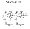
- Fig. 3 is a circuit diagram of the power amplifier 15.
- the power amplifier 15 is formed in a monolithic microwave integrated circuit (MMIC) formation, and is comprised of two amplifier circuits 24 and 25, an input terminal 23 and an output terminal 26.
- An input signal IN is applied to the input terminal 23, and an output signal OUT is output via the output terminal 26.
- MMIC monolithic microwave integrated circuit
- the amplifier circuit 24 includes a depletion type Shottky gate field effect transistor (so called D-type MESFET) 27, which functions as an amplifying element, and a capacitance element (capacitor) 28 preventing a DC component from being applied to the amplifier circuit 25.
- the amplifier circuit 24 includes a drain voltage input terminal 29 supplied with a positive drain voltage VDD1 from a drain voltage source. The voltage VDD1 is equal to, for example, +4 V.
- the amplifier circuit 24 includes a gate bias circuit 30, which supplies the gate of the D-type MESFET 27 with a negative gate bias voltage VGB1 equal to, for example, -1.5 V.
- the amplifier circuit 24 includes a gate bias source voltage input terminal 31 supplied with a negative gate bias source voltage VGG1 from a gate bias source. The voltage VGG1 is equal to, for example, -4.0 V.
- the amplifier circuit 24 includes resistors 32 and 33, which divide the gate bias source voltage VGG1 to thereby generate a gate bias voltage VGB1.
- the amplifier circuit 25 includes a D-type MESFET 34, which functions as an amplifying element, and a capacitance element (capacitor) 35 preventing a DC component from being applied to the output terminal 26.
- the amplifier circuit 25 includes a drain voltage input terminal 36 supplied with a positive drain voltage VDD2 supplied from a drain voltage source.
- the voltage VDD2 is equal to, for example, +5.8 V.
- the amplifier circuit 25 includes a gate bias circuit 37, which supplies the gate of the D-type MESFET 34 with a negative gate bias source voltage VGG2 equal to, for example, -4.0 V.
- the amplifier circuit 25 includes resistors 39 and 40, which divide the gate bias source voltage VGG2 to thereby generate a gate bias voltage VGB2.
- the portable telephone set as described above employs the power amplifier 15 of the transmit circuit part 7 of the high frequency circuit part 3, the power amplifier 15 using the D-type MESFETs 27 and 34.
- This structure requires the positive power sources respectively functioning as the drain voltage sources for the D-type MESFETs 27 and 34 and the negative power sources respectively functioning as the gate bias sources for the D-type MESFETs 27 and 34.
- a DC-DC converter is used to realize the positive and negative power sources. This increases the production cost and prevents down sizing.
- EP-A-0 561 346 discloses an amplifier circuit according to the preamble of claim 1, and employing a control voltage less than 0 V.
- a more specific object of the present invention is to provide an amplifier circuit and a multistage amplifier circuit which requires only a positive power source and does not require any negative power source.
- an amplifier circuit comprising:
- the first and second FETs are of the enhancement type in which the drain voltage and the control voltages are positive voltages. This requires only a positive power source, and does not require a negative power source.
- the second FET may be possible to omit the second FET and configure the amplifier circuit so that the control signal is supplied, as the gate bias voltage, to the gate of the first FET.
- the control signal is supplied, as the gate bias voltage, to the gate of the first FET.
- the above case increases power consumption in the inactive state.
- the second FET is provided with the gate supplied with the control signal.
- the amplifier circuit may be configured so that the gate of the first FET is supplied, as the gate bias voltage, with a voltage obtained by dividing the source voltage of the second FET by resistors. It is thus possible to set the gate bias voltage of the first FET closer to 0 V and further reduce power consumption.
- a multistage amplifier circuit comprising:
- the second-stage amplifier circuit of the amplifier circuit uses the enhancement-type FETs only. Hence, if the first-stage amplifier circuit is formed by enhancement-type FETs only, the drain voltages and the control signals are positive voltages, which can be generated by a positive voltage source. That is, a negative voltage source is not required.
- the second-stage amplifier circuit without the second FET so that the control signal is supplied, as the gate bias signal, to the gate of the first FET.
- the control signal is supplied, as the gate bias signal, to the gate of the first FET.
- the above case increases power consumption in the inactive state.
- the second FET with the gate supplied with the control signal.
- the multistage amplifier may further comprise a capacitance element provided between the first-stage amplifier circuit and the second-stage amplifier circuit.
- the multistage amplifier may be configured so that another control signal for controlling a gain of the second-stage amplifier circuit is applied to the second-stage amplifier circuit.
- the multistage amplifier circuit may be configured so that the control signal supplied to the gate of the second FET and the above-discussed other control signal are provided as a common signal.
- the multistage amplifier circuit may further comprise an impedance element provided between the gate of the second FET and an input terminal of the second-stage amplifier circuit to which the common signal is applied.
- the FETs can be MESFETs using, for example, compound semiconductor elements.
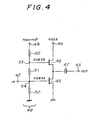
- Fig. 4 is a circuit diagram of a first amplifier circuit which is useful for understanding the present invention.
- the amplifier circuit shown in Fig. 4 includes a signal input terminal 42, a signal output terminal 43, and a drain voltage input terminal 44.
- An input signal IN is applied to the signal input terminal 42.
- An output signal is output via the signal output terminal 43.
- a positive drain voltage VDD3 is applied to the drain voltage input terminal 44.
- the amplifier circuit shown in Fig. 4 includes an enhancement-type Shottky field effect transistor (a so-called E-type MESFET) 45, which functions as an amplifying element.
- the amplifier circuit further includes an E-type MESFETs 46 which controls the drain voltage of the E-type MESFET 45, and a capacitance element (capacitor) 47 preventing a DC component from being applied to the output terminal 43.
- the gate of the E-type MESFET 45 is connected to the signal input terminal 42, and the drain thereof is connected to the source of the E-type MESFET 46 and to the signal output terminal 43 via the capacitance element 47.
- the source of the E-type MESFET 45 is grounded.
- the drain of the E-type MESFET 46 is connected to the drain voltage input terminal 44.
- the amplifier circuit shown in Fig. 4 includes a gate bias circuit 48, which supplies gate bias voltages VGB3A and VGB3B to the gates of the E-type MESFETs 45 and 46, respectively.
- the amplifier circuit includes a gate bias control voltage input terminal 49, to which a variable positive gate bias control voltage V control1 is applied as a control signal.
- the circuit 48 includes resistors 50, 51 and 52, which divide the gate bias control voltage V control1 to thereby generate the gate bias voltages VGB3A and VGB3B.
- the first amplifier circuit is based on the assumption that the gate bias control voltage source which outputs the gate bias control voltage V control1 is not capable of generating 0 V and the lower limit of the voltage V control1 is equal to, for example, 0.2 V.
- the resistors 50, 51 and 52 are connected in series between the gate bias control voltage input terminal 49 and the ground.
- a connection node 53 between the resistors 50 and 51 is connected to the gate of the E-type MESFET 46, and a connection node 54 between the resistors 51 and 52 is connected to the gate of the E-type MESFET 45.
- the amplifier circuit thus configured can control the gain by varying the gate bias control voltage V control1 in an active state thereof. More particularly, for example, as the voltage value of the gate bias control voltage V control1 is increased, the gate bias voltage VGB3B is increased, and the ON resistance of the E-type MESFET 46 is decreased. Further, the drain voltage of the E-type MESFET 45 is increased, and the gate bias voltage VGB3A is increased. Hence, the output level is increased.
- the gate bias control voltage V control1 As the voltage value of the gate bias control voltage V control1 is decreased, the gate bias voltage VGB3B is decreased, and the ON resistance of the E-type MESFET 46 is increased. Further, the drain voltage of the E-type MESFET 45 is decreased, and the gate bias voltage VGB3A is decreased. Hence, the output level is decreased.
- the first amplifier circuit determines the value of the drain voltage VDD3, the characteristic of the E-type MESFET 46 and the resistance values of the resistors 50, 51 and 52 so that in response to a variation of the gate bias control voltage V control1 , the drain voltage of the E-type MESFET 45 is changed between 4 V and 0 V, and the gate bias voltage VGB3A is changed between 0.4 V and 0 V.
- an amplifier circuit may be configured without the E-type MESFET 46.
- the gain can be controlled by varying the gate bias voltage VGB3A of the E-type MESFET 45.
- VGB3A of the E-type MESFET 45 it is impossible to increase the threshold voltage of the E-type MESFET 45.
- the gate bias voltage VGB3A of the E-type MESFET 45 is decreased to approximately 0 V, it is impossible to set the E-type MESFET 45 to the OFF state or a state close thereto.
- a large variable gain range cannot be obtained. If there is a requirement to greatly attenuate the input signal IN, the above configuration cannot meet the requirement.
- the first amplifier circuit is capable of realizing a large variable gain range and greatly attenuating the input signal IN.
- the E-type MESFET 46 can vary the value of the gate bias control voltage V control1 and thus vary the drain voltage of the E-type MESFET 45 so that the drain voltage of the E-type MESFET 45 can be decreased to 0 V.
- Fig. 5 is a diagram explaining the function and effects of the amplifier circuit according to Fig. 4 .
- a reference number 56 indicates a signal input terminal to which the input signal IN is applied.
- a reference number 57 indicates a signal output terminal via which the output signal OUT is output.
- a reference number 58 indicates a drain voltage input terminal to which a positive drain voltage VDD4 is applied.
- a reference number 59 indicates an E-type MESFET functioning as an amplifying element.
- a reference number 60 indicates a capacitance element which prevents a DC component from being applied to the signal output terminal 57.
- a reference number 61 indicates a gate bias circuit, which supplies the gate of the E-type MESFET 59 with a gate bias voltage VGB4.
- a reference number 62 indicates a gate bias source voltage input terminal, to which a positive gate bias voltage VGG4 is input.
- Reference numbers 63 and 64 indicate resistors, which divide the gate bias source voltage VGG4 to thereby generate the gate bias voltage VGB4.
- the drain voltage of the E-type MESFET 45 can be changed between 4 V and 0 V by varying the gate bias control voltage V control1 Further, the output level Pout can be varied over 30 dBc because the gate bias voltage VGB3A can be changed in the range of 0.4 V to 0 V.
- the gate bias control voltage V control1 is decreased to the lower limit, and the drain voltage of the E-type MESFET 45 and the gate bias voltage VGB3A are fixed to 0 V.
- the drain voltage of the E-type MESFET 45 and the gate bias voltage VGB3A are fixed to 0 V.
- the first amplifier circuit only positive voltages such as the drain voltage VDD3 and the gate bias control voltage V control1 , are used and any negative voltages are not needed, because only the E-type MESFET is used. Hence, it is necessary to provide only a positive power source, while a negative power source is not needed.
- Fig. 7 of a second amplifier circuit which is useful for understanding the present invention.
- the source of the E-type MESFET 46 is coupled to the drain of the E-type MESFET 46 via an inductance element 67.
- the other portions of the amplifier circuit shown in Fig. 7 are the same as those of the amplifier circuit according to Fig. 4 ..
- the inductance element 67 functions to prevent the signal amplified by the E-type MESFET 45 from leaking to the side of the drain voltage source via the E-type MESFET 46. In the dc formation, the source of the E-type MESFET 46 is shortcircuited and connected to the drain of the E-type MESFET 45.
- the second amplifier circuit has the same effects as those of the first amplifier circuit, and has an additional advantage in that the signal amplified by the E-type MESFET 45 can be prevented from leaking to the drain voltage source via the E-type MESFET 46 and can be efficiently transferred to the next-stage circuit.
- Fig. 8 A description will now be given, with reference to Fig. 8 , of a third amplifier circuit.
- Fig. 8 parts that are the same as those shown in the previously described figures are given the same reference numbers.
- the source of the E-type MESFET 46 is grounded via a capacitance element 68.
- the other circuit portions are the same as those of the circuit shown in Fig. 7 .
- the capacitance element 68 causes signals having frequencies lower than the signal to be amplified by the E-type MESFET 45 and noise applied from the drain voltage source via the drain voltage input terminal 44 to flow to the ground.
- the third amplifier circuit thus configured has the advantages as those of the second amplifier circuit and an additional advantage in that signals having frequencies lower than the signal to be amplified by the E-type MESFET 45 and noise applied from the drain voltage source via the drain voltage input terminal 44 can be prevented from being transferred to the next-stage circuit.
- Fig. 9 A description will now be given, with reference to Fig. 9 , of a fourth amplifier circuit.
- the source of the E-type MESFET 46 is coupled to the drain of the E-type MESFET 45 via a parallel resonation circuit 69.
- the other circuit portions of the circuit shown in Fig. 9 are the same as those of the circuit according to Fig. 4 .
- the parallel resonation circuit 69 is made up of an inductance element 70 and a capacitance element 71, and resonates at a frequency of the signal to be amplified by the E-type MESFET 45.
- the fourth amplifier circuit has the same advantages as those of the first amplifier circuit and another advantage in that signals having frequencies other than the frequency of the signal to be amplified by the E-type MESFET 45 can be prevented from being transferred to the next-stage circuit, so that the selectivity can be improved.
- the fifth amplifier circuit includes a gate bias circuit 73 having a configuration different from that of the gate bias circuit 48 of tFig. 4.
- the other circuit portions are the same as those of Fig. 4 .
- the gate bias circuit 73 includes a gate bias source voltage input terminal 74, a gate bias control voltage input terminal 75, an E-type MESFET 76, and resistors 77, 78 and 79.
- a positive gate bias source voltage VGG3 from a gate bias source is applied to the gate bias source voltage input terminal 74.
- a positive gate bias control voltage V control2 which controls the gate bias voltages VGB3A and VGB3B is applied to the gate bias control voltage input terminal 75.
- the control voltage V control2 is a variable voltage for controlling the gate bias voltages VGB3A and VGB3B.
- the E-type MESFET 76 controls the gate bias voltages VGB3A and VGB3B.
- the fifth amplifier circuit is based on the assumption that the gate bias control voltage source which outputs the gate bias control voltage V control2 is not capable of generating 0 V and the lower limit of the voltage V control2 is equal to, for example, 0.2 V.
- the E-type MESFET 76 has a drain connected to the gate bias source voltage input terminal 74, and a gate connected to the gate bias control voltage input terminal 75.
- the resistors 77, 78 and 79 are connected in series between the source of the E-type MESFET 76 and the ground.
- a connection node 80 between the resistors 77 and 78 is connected to the gate of the E-type MESFET 46, and a connection node 81 between the resistors 78 and 79 is connected to the gate of the E-type MESFET 45.
- the gate bias control voltage V control2 in the active state. For example, as the value of the gate bias control voltage V control2 is increased, the ON resistance of the E-type MESFET 76 is decreased, and the current flowing in the resistors 77 - 79 is increased. Further, the gate bias voltage VGB3B of the E-type MESFET 46 is increased, and the ON resistance of the E type MESFET 46 is decreased. The drain voltage of the E-type MESFET 45 is increased and the gate bias voltage VGB3A is increased. As a result, the output level is increased.
- the ON resistance of the E-type MESFET 76 is increased, and the current flowing in the resistors 77 - 79 is decreased.
- the gate bias voltage VGB3B of the E-type MESFET 46 is decreased, and the ON resistance of the E-type MESFET 46 is increased.
- the drain voltage of the E-type MESFET 45 is decreased, and the gate bias voltage VGB3A is decreased. Hence, the output level is decreased.
- the fifth amplifier circuit determines the value of the gate bias source voltage VGG3, the characteristics of the E-type MESFETs 46 and 47 and the resistance values of the resistors 77, 78 and 79 so that in response to a variation of the gate bias control voltage V control2 the drain voltage of the E-type MESFET 45 is changed between 4 V and 0 V, and the gate bias voltage VGB3A is changed between 0.4 V and 0 V.
- the gate bias control voltage V control2 is decreased to the lower limit, and the drain voltage of the E-type MESFET 45 and the gate bias voltage VGB3A are fixed to O V. Hence, even if the input signal IN is applied to the E-type MESFET 45, the drain current cannot flow in the E-type MESFET 45.
- the fifth amplifier circuit only positive voltages such as the drain voltage VDD3, the gate bias source voltage VGG3 and the gate bias control voltage V control2 , and any negative voltages are not needed, because only the E-type MESFETs are used. Hence, it is necessary to provide only a positive power source, while a negative power source is not needed.
- an inductance element provided between the source of the E-type MESFET 46 and the drain of the E-type MESFET 45. In this case, it is possible to prevent the signal amplified by the E-type MESFET 45 from leaking to the drain voltage source via the E-type MESFET 46 and to efficiently transfer the signal amplified by the E-type MESFET 45 to the next-stage circuit.
- the parallel resonance circuit resonates at the frequency, of the signal to be amplified by the E-type MESFET 45, and prevents signals other than the desired signal from being transferred to the next-stage circuit. Hence, the selectivity can be improved.
- FIG. 11 A description will now be given, with reference to Fig. 11 , of a sixth amplifier circuit.
- the sixth amplifier circuit employs a gate bias circuit 83 having a configuration different from that of the gate bias circuit 48 used in Fig. 4 .
- the other parts are the same as those of Fig. 4 .
- the gate bias circuit 83 includes a gate bias source voltage input terminal 84, a gate bias control voltage input terminal 85, an E-type MESFET 86, and resistors 87, 88 and 89.
- the positive gate bias source voltage VGG3 from the gate bias source is applied to the gate bias source voltage input terminal 84.
- a positive gate bias control voltage V control3 which controls the gate bias voltages VGB3A and VGB3B is applied to the gate bias control voltage input terminal 85.
- the control voltage Vcontrol3 is a variable voltage for controlling the gate bias voltages VGB3A and VGB3B.
- the E-type MESFET 86 controls the gate bias voltages VGB3A and VGB3B.
- the sixth amplifier circuit is based on the assumption that the gate bias control voltage source which outputs the gate bias control voltage V control3 is not capable of generating 0 V and the lower limit of the voltage V control3 is equal to, for example, 0.2 V.
- the drain of the E-type MESFET 86 is connected to the gate bias source voltage input terminal 84, and the gate thereof is connected to the gate bias control voltage input terminal 85, which is connected to the gate of the E-type MESFET 46 via the resistor 87.
- the resistors 88 and 89 are connected in series between the source of the E-type MESFET 86 and the ground.
- a connection node 90 between the resistors 88 and 89 is connected to the gate of the E-type MESFET 45.
- the gate bias control voltage V control3 in the active state. For example, as the value of the gate bias control voltage Vcontrol3 is increased, the gate bias VGB3B of the E-type MESFET 46 is increased, and the ON resistance of the E-type MESFET 46 is decreased. Further, the drain voltage of the E-type MESFET 45 is increased and the ON resistance of the E-type MESFET 86 is decreased. The current flowing in the resistors 88 and 89 is increased, and the gate bias voltage VGB3A is increased. Hence, the output level is increased.
- the gate bias control voltage Vcontrol3 As the gate bias control voltage Vcontrol3 is decreased, the gate bias voltage VGB3B of the E-type MESFET 46 is decreased, and the ON resistance of the E-type MESFET 46 is increased. Further, the drain voltage of the E-type MESFET 45 is decreased, and the ON resistance of the E-type MESFET 86 is increased. Hence, the current flowing in the resistors 88 and 89 is reduced, and the gate bias voltage VGB3A is decreased. Hence, the output level is decreased.
- the sixth eamplifier circuit determines the value of the gate bias source voltage VGG3, the characteristics of the E-type MESFE 46 and 48 and the resistance values of the resistors 87, 88 and 89 so that in response to a variation of the gate bias control voltage V control3 , the drain voltage of the E-type MESFET 45 is changed between 4 V and 0 V, and the gate bias voltage VGB3A is changed between 0.4 V and 0 V.
- the gate bias control voltage V control3 is decreased to the lower limit, and the drain voltage of the E-type MESFET 45 and the gate bias voltage VGB3A are fixed to 0 V. Hence, even if the input signal IN is applied to the E-type MESFET 45, the drain current cannot flow in the E-type MESFET 45.
- the sixth amplifier circuit only positive voltages such as the drain voltage VDD3, the gate bias source voltage VGG3 and the gate bias control voltage V control3 , and any negative voltages are not needed, because only the E-type MESFETs are used. Hence, it is necessary to provide only a positive power source, while a negative power source is not needed.
- an inductance element provided between the source of the E-type MESFET 46 and the drain of the E-type MESFET 45. In this case, it is possible to prevent the signal amplified by the E-type MESFET 45 from leaking to the drain voltage source via the E-type MESFET 46 and to efficiently transfer the signal amplified by the E-type MESFET 45 to the next-stage circuit.
- the parallel resonance circuit resonates at the frequency of the signal to be amplified by the E-type MESFET 45, and prevents signals other than the desired signal from being transferred to the next-stage circuit. Hence, the selectivity can be improved.
- the amplifier circuit shown in Fig. 12 includes a signal input terminal 92, a signal output terminal 93, a drain voltage input terminal 94, an E-type MESFET functioning as an amplifying element, and a capacitance element 96 for DC isolation.
- a positive drain voltage VDD5 is applied to the drain voltage input terminal 94.
- the gate of the E-type MESFET 95 is connected to the signal input terminal 92, and the drain thereof is connected to the drain voltage input terminal 94 and to the signal output terminal 93 via the capacitance element 96.
- the amplifier circuit shown in Fig. 12 includes a gate bias circuit 97, which supplies the gate of the E-type MESFET 95 with a positive gate bias voltage VGB5.
- the circuit 97 includes a gate bias source voltage input terminal 98 via which a positive gate bias source voltage VGG5 is supplied.
- the circuit 97 has a gate bias control voltage input terminal 99, an E-type MESFET 100, and resistors 101 and 102.
- a positive gate bias control voltage V contro14 having a variable voltage value is applied to the terminal 99 as a control signal for controlling the gate bias voltage VGB5.
- the E-type MESFET 100 controls the gate bias voltage VGB5.
- the amplifier circuit shown in Figure 12 is configured on the assumption that the gate bias control voltage source which outputs the gate bias control voltage V control4 is not capable of generating 0 V and the lower limit of the voltage V control4 is equal to, for example, 0.2 V.
- the drain of the E-type MESFET 100 is connected to the gate bias source voltage input terminal 98, and the gate thereof is connected to the bias control voltage input terminal 99.
- the resistors 101 and 102 are connected in series between the source of the E-type MESFET 100 and the ground.
- a connection node 103 between the resistors 101 and 102 is connected to the gate of the E-type MESFET 95.
- the gain by varying the gate bias control voltage V control4 in the active state. For example, as the value of the gate bias control voltage V control4 is increased, the ON resistance of the E-type MESFET 100 is decreased, and the current flowing in the resistors 101 and 102 is increased. Further, the gate bias voltage VGB5 of the E-type MESFET 95 is increased, and the output level is increased.
- the gate bias control voltage V control4 As the value of the gate bias control voltage V control4 is reduced, the ON resistance of the E-type MESFET 100 is increased, and the current flowing in the resistors 101 and 102 is decreased.
- the gate bias voltage VGB5 of the E-type MESFET 95 is decreased, and the output level is reduced.
- the amplifier circuit of Figure 12 determines the value of the gate bias source voltage VGG5, the characteristic of the E-type MESFET 100 and the resistance values of the resistors 101 and 102 so that the following conditions are satisfied.
- the gate bias control voltage V control4 can be varied between 2.5 V and 0.2 V. When the gate bias control voltage V control4 is equal to 2.5 V, the gate bias voltage VGB5 is equal to 0.5 V. When the gate bias control voltage V control4 is equal to 0.2 V, the gate bias voltage VGB5 is close to 0 V.
- the gate bias control voltage V control4 is set to 0.2 V.
- the gate bias voltage VGB5 can be set close to 0 V, and it is thus possible to set the drain current flowing in the E-type MESFET 95 equal to or lower than tens of microamperes.
- the gate of the E-type MESFET 95 In order to reduce the current flowing in the drain of the E-type MESFET 95 to a value as small as possible in the inactive state, it is necessary to supply the gate of the E-type MESFET 95 with a voltage ch lower than the threshold voltage thereof, that a voltage as close to 0 V as possible. If the above cannot be performed, the drain current will be increased and the power consumption will also be increased.
- the gate bias source voltage VGG4 cannot be reduced until the gate bias voltage VGB4 is set equal to 0 V. In this case, it is impossible to reduce power consumption.
- the gate bias voltage VGB5 can be made close to 0 V by setting the gate bias control voltage V contro14 equal to 0.2 V. Hence, it is possible to set the drain current flowing in the E-type MESFET 95 equal to or lower than tens of microamperes and to thus reduce power consumption.
- a current IGG flowing in the gate of the E-type MESFET 59 in a saturated output operation is approximately twice or three times the current flowing when a D-type MESFET is used.
- the gate current IGG of 10 - 20 mA flows.
- the gate bias VGB4 is decreased due to a voltage drop developing across the resistor 63 through which the gate current IGG4 flows. In this case, the circuit will shift to a state in which the output level is decreased.
- the resistors 63 and 64 have sufficiently small values, a decrease in the gate bias voltage VGB4 can be suppressed even if the gate current IGG4 is large.
- the resistance values of the resistors 63 and 64 are too small, a sufficient current cannot be supplied to the resistors 63 and 64 due to the current supply ability of the gate bias source. Even if the current supply ability of the gate bias source can be increased, a large current flows in the resistors 63 and 64 with the gate bias voltage VGB4 applied. Hence, power consumption cannot be reduced.
- the gate bias control voltage V control4 can be set equal to 0.2 V in the inactive state even if the resistance values of the resistors 101 and 102 are sufficiently reduced so that a large current is allowed to flow therein and a decrease in the gate bias voltage VGB5 caused by the current flowing to the gate of the E-type MESFET 95 is prevented.
- the current flowing in the resistors 101 and 102 can be reduced and power consumption can be reduced.
- the automatic power control voltage Vapc can be varied within a range of approximately 0.2 V to 2.5 V, and the upper limit of an automatic power control current Iapc is approximately equal to 5 mA. It is assumed that when the automatic power control voltage Vapc is equal to 2.5 V, the voltage applied across the gate and source of the E-type MESFET 59 in operation is 0.5 V. In this case, it is required that the ratio of the resistance value of the resistor 63 to that of the resistor 64 is 4 : 1.
- the minimum value of the sum of the resistance values of the resistors 63 and 64 is obtained by Vapc-max/Iapc-max, and is equal to 500 ⁇ . Hence, the above sum becomes greater than 500 ⁇ , and the resistance value of the resistor 63 is greater than 400 n.
- the current IGG4 flowing to the gate of the E-type MESFET 59 is determined as follows.
- the value obtained by (the resistance value of the resistor 63) x IGG4 is less than 0.1 V.
- IGG4 is less than (0.1 V /400 ⁇ ), namely, 0.25 mA.
- the current IGG4 flowing in the gate and source of the E-type MESFET 59 is equal to or greater than 0.5 mA, the tolerable variation value of the voltage between the gate and source of the E-type MESFET 59 exceeds 0.1 V.
- the configuration according to Figure 12 is required.
- the first embodiment of the present invention employs only the E-type MESFETs, and thus the drain voltage VDD5, the gate bias source voltage VGG5 and the gate bias control voltage V control4 are positive voltages, which can be produced by a positive power source. That is, no negative power source is needed.
- Fig. 13 is a circuit diagram of a multistage amplifier circuit according to the second embodiment of the present invention, which is applied to the power amplifier of the transmit circuit part of the portable telephone set.
- the input signal (high frequency signal) IN is applied to a signal input terminal 106.
- An output signal (high frequency signal) OUT is output via a signal output terminal OUT.
- a capacitance element 108 prevents a DC component from DC isolation.
- a gate bias control voltage generating circuit 112 generates a gate bias control voltage v contro15 to be supplied to the amplifier circuits 109, 110 and 111.
- the circuit 112 is configured as follows.
- the automatic power control voltage Vapc is applied to an automatic power control voltage input terminal 113.
- the voltage Vapc serves as a control signal which automatically controls the output level of the output signal OUT supplied from a control circuit part (not shown) of the portable telephone set.
- the circuit 112 includes two resistors 114 and 115 dividing the automatic power control voltage Vapc.
- the gate bias control voltage V contro15 is obtained at a connection node 116 between the resistors 114 and 115.
- a gate bias control voltage line 117 is connected to the connection node 116.
- the amplifier circuit 109 is configured as follows.
- a positive drain voltage VDD6 is applied to a drain voltage input terminal 118.
- An E-type MESFET 119 functions as an amplifying element.
- An E-type MESFET 120 controls the drain voltage of the E-type MESFET 119.
- a capacitance element 121 is used for DC isolation.
- An inductance element 122 is provided between the source of the E-type MESFET 120 and the drain of the E-type MESFET 119.
- the gate of the E-type MESFET 119 is connected to the signal input terminal 106 via the capacitance element 108, and the drain thereof is connected to the source of the E-type MESFET 120 via the inductance element 122 and to one end of the capacitance element 121.
- the source of the E-type MESFET 119 is grounded.
- the drain of the E-type MESFET 120 is connected to the drain voltage input terminal 118.
- the amplifier circuit 109 includes a gate bias circuit 123, which supplies positive gate bias voltages VGB6A and VGB6B to the gates of the E-type MESFETS 119 and 120.
- the circuit 123 includes resistors 124, 125 and 126, which divide the gate bias control voltage V control5 .
- the resistors 124, 125 and 126 are connected in series between the gate bias control voltage line 117 and the ground.
- a connection node 127 between the resistors 124 and 125 is connected to the gate of the E-type MESFET 120.
- a connection node 128 between the resistors 125 and 126 is connected to the gate of the E-type MESFET 119.
- the amplifier circuit 110 is configured as follows.
- the positive drain voltage VDD6 is applied to a drain voltage input terminal 129.
- An E-type MESFET 130 functions as an amplifying element.
- a capacitance element 131 is used for DC isolation.
- the gate of the E-type MESFET 130 is connected to the other end of the capacitance element 121, and the drain thereof is connected to the drain voltage input terminal 129 and one end of the capacitance element 131.
- the amplifier circuit 110 includes a gate bias circuit 132, which supplies a positive gate bias voltage VGB6C to the gate of the E-type MESFET 130.
- the circuit 132 has a gate bias source voltage input terminal to which the positive gate bias source voltage VGG6 is applied.
- the circuit 132 includes an E-type MESFET 134, which controls the gate bias voltage VGB6C, and resistors 135 and 136.
- the drain of the E-type MESFET 134 is connected to the gate bias source voltage input terminal 133, and the gate thereof is connected to the gate bias voltage line 117 via a resistor 138.
- the resistor 138 attenuates the signal output to the gate of the E-type MESFET 134 in order to prevent occurrence of oscillation. If the signal amplified by the E-type MESFET 119 is fed back to the amplifier circuit 109 via the capacitance element 121, the resistor 135 and the source and gate of the E-type MESFET 134, the circuit may oscillate.
- the resistors 135 and 136 are connected in series between the source of the E-type MESFET 134 and the ground.
- a connection node 137 between the resistors 135 and 136 is connected to the gate of the E-type MESFET 130.
- the amplifier circuit 111 has a drain voltage input terminal 139 to which the positive drain voltage VDD6 is applied, an E-type MESFET 140 functioning as an amplifying element, and a capacitance element 141 for DC isolation.
- the gate of the E-type MESFET 140 is connected to the other end of the capacitance element 131, and the drain thereof is connected to the drain voltage input terminal 139 and to the signal output terminal 107 via the capacitance element 141.
- the source of the E-type MESFET 140 is grounded.
- the amplifier circuit 111 includes a gate bias circuit 142, which supplies a positive gate bias voltage VGB6D to the gate of the E-type MESFET 140.
- the circuit 142 includes a gate bias source voltage input terminal 143, to which the positive gate bias source voltage VGG6 is applied.
- the circuit 142 includes an E-type MESFET 144 for controlling the gate bias voltage VGB6B, and resistors 145 and 146.
- the drain of the E-type MESFET 144 is connected to the gate bias source voltage input terminal 143, and the gate thereof is connected to the gate bias voltage line 117 via a resistor 147.
- the resistor 147 attenuates the signal output to the gate of the E-type MESFET 134 in order to prevent occurrence of oscillation. If the signal amplified by the E-type MESFET 130 is fed back to the amplifier circuits 109 and 110 via the capacitance element 131, the resistor 145 and the source and gate of the E-type MESFET 144 may oscillate.
- the resistors 145 and 146 are connected in series between the source of the E-type MESFET 144 and the ground.
- a connection node 148 between the resistors 145 and 146 is connected to the gate of the E-type MESFET 140.
- the first amplifier circuit 109 has the same configuration as that of the second embodiment of the present invention, and the amplifier circuits 110 and 111 of the second and third stages have the same configuration as that of the first embodiment of the present invention.
- the multistage amplifier circuit of the second embodiment of the present invention thus configured, it is possible to provide, as the automatic power control voltage Vapc, the voltage necessary to obtain the transmit output determined by the positional relationship (distance) between the portable telephone set and a ground station.
- Fig. 14 is a diagram explaining ranges of variations in the output levels of the amplifier circuits 109, 110 and 111.
- Fig. 14 denotes the positions of the output terminals of the amplifier circuits 109, 110 and 111, and the vertical axis denotes the output level.
- an arrow 151 indicates a variation range of the output level of the amplifier circuit 109.
- An arrow 152 indicates a variation range of the output level of the amplifier circuit 110.
- An arrow 153 indicates a variation range of the output level of the amplifier 111, that is, the output signal OUT.
- the amplifier circuits 110 and 111 of the second and third stages are configured as shown in Fig. 13 , it is necessary to set the variable range of the output level of the first-stage amplifier circuit 109 to be as large as 30 dBc in order to obtain a variable range of the output signal OUT of 60 dBc.
- the amplifier circuit 109 of the first stage has the same configuration as that Fig. 7 . Thus, it is possible to vary the output level over 30 dBc and greatly attenuate the input signal IN.
- the input/output characteristic of the amplifier circuit shown in Fig. 5 is as shown in Fig. 15 .
- a solid line 155 indicates a case where the gate bias voltage VGB4 of the E-type MESFET 59 is 0.4 V
- a broken line 156 indicates a case where the gate bias voltage VGB4 of the E-type MESFET 59 is 0.0 V.
- variable range of the output level Pout can be set greater than 20 dBc.
- the power amplifier of the portable telephone set employs the fixed input level Pin in order to make the structure as simple as possible and reduce the production cost.
- the amplifier circuit shown in Fig. 5 is not suitable for the amplifier circuit 109 of the first stage.
- the automatic power control voltage Vapc equal to 0.2 V is supplied when the portable telephone set is receiving a signal or waiting for receipt of a signal.
- the gate bias voltage VGB6B of the E-type MESFET 120 in the amplifier circuit 109 is decreased, and the drain voltage of the E-type MESFET 119 can be set equal to 0 V.
- the gate bias voltage VGB6A of the E-type MESFET 119 can be decreased close to 0 V.
- the drain current does not flow in the E-type MESFET 119.
- the gate voltage of the E-type MESFET 134 in the amplifier circuit 110 is decreased, so that the gate bias voltage VGB6C of the E-type MESFET 130 can be set close to 0 V. As a result, it is possible to reduce the drain current flowing in the E-type MESFET 130 to a very small value.
- the gate voltage of the E-type MESFET 144 in the amplifier circuit 111 is decreased, so that the gate bias voltage VGB6D of the E-type MESFET 140 can be set close to 0 V. As a result, it is possible to reduce the drain current flowing in the E-type MESFET 140 to a very small value.
- the second embodiment of the present invention employs only the E-type MESFETs which operate with the positive voltages, and thus use only the positive drain voltage VDD6, the positive gate bias source voltage VGG6 and the positive automatic power control voltage Vapc. In other words, the second embodiment of the present invention does not require any negative voltages. Hence, it is possible to realize cost reduction and down sizing for the portable telephone sets.
- the first-stage amplifier circuit 109 has the same structure as that of Fig.7 .
- the second-stage amplifier circuit 110 has the same structure as that of the first embodiment of the present invention shown in Fig. 12 . Hence,it is possible to reduce the current flowing in the resistors 135 and 136 in the E-type MESFET 134 at the time of receiving and waiting for a signal even if the resistors 135 and 136 are small so as to make a large current flow in these resistors and prevent the gate bias voltage VGB6C from being reduced by the current flowing to the gate of the E-type MESFET 130. Hence, it is possible to reduce power consumption.
- the third-stage amplifier circuit 111 has the same structure as that of the first embodiment of the present invention. Hence,it is possible to reduce the current flowing in the resistors 145 and 146 in the E-type MESFET 144 at the time of receiving and waiting for a signal even if the resistors 145 and 146 are small so as to make a large current flow in these resistors and prevent the gate bias voltage VGB6D from being reduced by the current flowing to the gate of the E-type MESFET 140. Hence, it is possible to reduce power consumption.
- the drain current does not flow in the E-type MESFET 119 and very small drain currents flow in the E-type MESFETs 130 and 140. From this point of view, power consumption can be reduced. Additionally, it is not necessary to use a switch module to shut the drain currents of the E-type MESFETs 119, 130 and 140 at the time of receiving or waiting for a signal. From this point of view, power consumption can be reduced and down sizing can be realized.
- the amplifier circuit 109 of the first stage can be configured so as to have the same configuration as any of the first to sixth, amplifier circuits described above.
- the resistors 114 and 115 connected in series between the automatic power control voltage input terminal 113 and the ground. In this case, the terminal 113 is directly connected to the gate bias control voltage line 117. It is also possible to omit the resistor 124 between the gate bias control voltage line 117 and the gate of the E-type MESFET 120. It is also possible to omit the resistor 135 provided between the source of the E-type MESFET 134 and the gate of the E-type MESFET 130 as well as the resistor 145 provided between the source of the E-type MESFET 144 and the gate of the E-type MESFET 140.
- resistor 138 provided between the gate of the E-type MESFET 134 and the gate bias control voltage line 117 and the resistor 144 provided between the gate of the E-type MESFET 144 and the line 117.
- the MESFETs used in the present invention are, for example, MESFETs using compound semiconductor elements.
Landscapes
- Engineering & Computer Science (AREA)
- Power Engineering (AREA)
- Amplifiers (AREA)
Description
- The present invention relates to amplifier circuits which employ field effect transistors (FETs).
-
Fig. 1 is a block diagram of a part of a conventional portable telephone set. The portable telephone set includes an input/output circuit part 1, abaseband circuit part 2, a high-frequency circuit part 3, anantenna 4 and apower supply part 5. - The input/
output circuit part 1 includes a keyboard, a display part, a microphone and a speaker. Thebaseband circuit part 2 converts an analog voice signal supplied from the microphone of the input/output circuit part 1 into a digital signal. Then, thebaseband circuit part 2 performs voice coding, channel coding, scrambling, and digital modulating processes. Finally, thebaseband circuit part 2 converts the processed digital signal into an analog signal, which is supplied to the high-frequency circuit part 3. Further, thebaseband circuit 2 converts an analog signal supplied from the high-frequency circuit part 3 into a digital signal. Then, thebaseband circuit 2 performs digital demodulating, descrambling, channel decoding and voice decoding operations. Then, thebaseband circuit part 2 supplies the resultant analog voice signal to the speaker of the input/output circuit part 1. - The high-
frequency circuit part 3 modulates the analog signal from thebaseband circuit part 2 and performs a power amplifying operation on the modulated signal. Also, the high-frequency circuit part 3 amplifies a signal received via theantenna 4 and demodulates the amplified signal. Thepower supply part 5 supplies electricity to the input/output circuit part 1, thebaseband circuit part 2 and the high-frequency circuit part 3. -
Fig. 2 is a circuit diagram of the configuration of the high-frequency circuit part 3. The high-frequency circuit part 3 includes atransmit circuit part 7, areceive circuit part 8 and aswitch circuit 9. Theswitch circuit 9 connects an output terminal 7A of thetransmit circuit part 7 to theantenna 4 at the time of transmitting a signal, and connects aninput terminal 8A of thereceive circuit part 8 to the antenna at the time of receiving a signal. - The
transmit circuit part 7 includes amodulator 10, a voltage-controlled oscillator (VCO) 11, amultiplier 12, anamplifier 13, a surface acoustic wave (SAW)filter 14, and apower amplifier 15. Themodulator 10 modulates the signal supplied from thebaseband circuit part 2. The VCO 11 generates a signal necessary to perform an up conversion of the signal output by themodulator 10. Themultiplier 12 multiplies the signal from themodulator 10 by the signal from the VCO 11 so that the modulated signal is changed to a high-frequency signal. Theamplifier 13 amplifies the high-frequency signal output from themultiplier 12. The SAW filter 14 functions as a band-pass filter and filters the amplified high-frequency signal. Thepower amplifier 15 performs a power amplifying operation on the amplified high-frequency signal. - The
receive circuit part 8 includes anamplifier 16, a SAW filter 17, aVCO 18, anamplifier 19, amultiplier 20 and ademodulator 21. Theamplifier 16 amplifies the signal received via theantenna 4. The SAW filter 17 functions as a bandpass filter and filters the amplified received signal. TheVCO 18 generates a signal necessary to perform a down conversion on the signal from the SAW filter 17. Theamplifier 19 amplifies the signal output by theVCO 18. The multiplier multiplies the signal from the SAW filter 17 by the amplified signal from theamplifier 19 so that the baseband signal of the received signal can be retrieved. Thedemodulator 10 demodulates the output signal of themultiplier 20 and reproduces the original signal. -
Fig. 3 is a circuit diagram of thepower amplifier 15. Thepower amplifier 15 is formed in a monolithic microwave integrated circuit (MMIC) formation, and is comprised of twoamplifier circuits input terminal 23 and anoutput terminal 26. An input signal IN is applied to theinput terminal 23, and an output signal OUT is output via theoutput terminal 26. - The
amplifier circuit 24 includes a depletion type Shottky gate field effect transistor (so called D-type MESFET) 27, which functions as an amplifying element, and a capacitance element (capacitor) 28 preventing a DC component from being applied to theamplifier circuit 25. Theamplifier circuit 24 includes a drainvoltage input terminal 29 supplied with a positive drain voltage VDD1 from a drain voltage source. The voltage VDD1 is equal to, for example, +4 V. Theamplifier circuit 24 includes agate bias circuit 30, which supplies the gate of the D-type MESFET 27 with a negative gate bias voltage VGB1 equal to, for example, -1.5 V. Theamplifier circuit 24 includes a gate bias sourcevoltage input terminal 31 supplied with a negative gate bias source voltage VGG1 from a gate bias source. The voltage VGG1 is equal to, for example, -4.0 V. Theamplifier circuit 24 includesresistors - The
amplifier circuit 25 includes a D-type MESFET 34, which functions as an amplifying element, and a capacitance element (capacitor) 35 preventing a DC component from being applied to theoutput terminal 26. Theamplifier circuit 25 includes a drain voltage input terminal 36 supplied with a positive drain voltage VDD2 supplied from a drain voltage source. The voltage VDD2 is equal to, for example, +5.8 V. Theamplifier circuit 25 includes agate bias circuit 37, which supplies the gate of the D-type MESFET 34 with a negative gate bias source voltage VGG2 equal to, for example, -4.0 V. Theamplifier circuit 25 includesresistors - The portable telephone set as described above employs the
power amplifier 15 of thetransmit circuit part 7 of the highfrequency circuit part 3, thepower amplifier 15 using the D-type MESFETs type MESFETs type MESFETs -
EP-A-0 561 346 discloses an amplifier circuit according to the preamble ofclaim 1, and employing a control voltage less than 0 V. - It is a general object of the present invention to eliminate the above disadvantages.
- A more specific object of the present invention is to provide an amplifier circuit and a multistage amplifier circuit which requires only a positive power source and does not require any negative power source.
- According to a first aspect of the invention, there is provided an amplifier circuit comprising:
- a first FET of an enhancement type having a source, a gate supplied with an input signal and a gate bias voltage, and a drain via which an amplified output signal is output, thereby forming a current path directed to the source from the gate;
- a second FET of the enhancement type having a drain connected to a gate bias supply source for the first FET, a gate supplied with a control signal, and a source via which a source voltage controlled by the control signal is output, the source voltage being supplied to the gate of the first FET as the gate bias voltage; and
- a resistance element having a first end connected to the source of the second FET and the gate of the first FET, and having a second end grounded; characterized in that:
- said amplifier circuit requires only a positive power source.
- According to the above amplifier circuit, the first and second FETs are of the enhancement type in which the drain voltage and the control voltages are positive voltages. This requires only a positive power source, and does not require a negative power source.
- It is possible to vary the gate bias voltage of the first FET and thus control the gain of the amplifier circuit by varying the level of the control signal in an active state.
- It may be possible to omit the second FET and configure the amplifier circuit so that the control signal is supplied, as the gate bias voltage, to the gate of the first FET. In this case, it is desired to reduce the resistance value of the resistance element in order to cause a current much greater than the current flowing in the gate of the first FET to flow in the resistance element because the gate voltage is decreased and the output level is thus reduced if a large current flows to the gate of the first FET. However, the above case increases power consumption in the inactive state.
- According to the present invention having the above structure, the second FET is provided with the gate supplied with the control signal. Hence it is possible to reduce the current flowing in the resistance element and set the gate bias voltage of the first FET close to 0 V due to the function of the second FET even if the current flowing in the resistance element is increased in the active state in order to prevent a decrease in the gate bias voltage of the first FET or the control signal cannot be set to 0 V in the inactive state. As a result, the drain current of the first FET can be reduced and thus power consumption can be reduced.
- The amplifier circuit may be configured so that the gate of the first FET is supplied, as the gate bias voltage, with a voltage obtained by dividing the source voltage of the second FET by resistors. It is thus possible to set the gate bias voltage of the first FET closer to 0 V and further reduce power consumption.
- According to a second aspect of the invention, there is provided a multistage amplifier circuit comprising:
- a first-stage amplifier circuit amplifying an input signal; and
- a second-stage amplifier circuit including a first FET of an enhancement type having a source, a gate supplied with an input signal and a gate bias voltage, and a drain via which an amplified output signal is output, thereby forming a current path directed to the source from the gate, and a second FET of the enhancement type having a drain connected to a gate bias supply source for the first FET, a gate supplied with a control signal, and a source via which a source voltage controlled by the control signal is output, the source voltage being supplied to the gate of the first FET as the gate bias voltage; and
- a resistance element having a first end connected to the source of the second FET and the gate of the first FET, and having a second end grounded;
- The second-stage amplifier circuit of the amplifier circuit uses the enhancement-type FETs only. Hence, if the first-stage amplifier circuit is formed by enhancement-type FETs only, the drain voltages and the control signals are positive voltages, which can be generated by a positive voltage source. That is, a negative voltage source is not required.
- It may be possible to configure the second-stage amplifier circuit without the second FET so that the control signal is supplied, as the gate bias signal, to the gate of the first FET. However, in this case, it is desired to reduce the resistance value of the resistance element in order to cause a current much greater than the current flowing in the gate of the first FET to flow in the resistance element because the gate voltage is decreased and the output level is thus reduced if a large current flows to the gate of the first FET. However, the above case increases power consumption in the inactive state.
- According to the present invention having the above structure, there is provided the second FET with the gate supplied with the control signal. Hence it is possible to reduce the current flowing in the resistance element and set the gate bias voltage of the first FET close to 0 V due to the function of the second FET even if the current flowing in the resistance element is increased in the active state in order to prevent a decrease in the gate bias voltage of the first FET or the control signal cannot be set to 0 V in the inactive state. As a result, the drain current of the first FET can be reduced and thus power consumption can be reduced.
- The multistage amplifier may further comprise a capacitance element provided between the first-stage amplifier circuit and the second-stage amplifier circuit.
- The multistage amplifier may be configured so that another control signal for controlling a gain of the second-stage amplifier circuit is applied to the second-stage amplifier circuit.
- The multistage amplifier circuit may be configured so that the control signal supplied to the gate of the second FET and the above-discussed other control signal are provided as a common signal.
- The multistage amplifier circuit may further comprise an impedance element provided between the gate of the second FET and an input terminal of the second-stage amplifier circuit to which the common signal is applied.
- In the above amplifier circuits, the FETs can be MESFETs using, for example, compound semiconductor elements.
- Other objects, features and advantages of the present invention will become more apparent from the following detailed description when read in conjunction with the accompanying drawings, in which:
-
Fig. 1 is a block diagram of an essential part of a conventional portable telephone set; -
Fig. 2 is a circuit diagram of a high frequency circuit part shown inFig. 1 ; -
Fig. 3 is a circuit diagram of a power amplifier shown inFig. 1 ; -
Fig. 4 is a circuit diagram of a first amplifier circuit useful for understanding the present invention; -
Fig. 5 is a circuit diagram explaining function and effects of the circuit shown inFig. 4 ; -
Fig. 6 is a graph of an output level vs drain voltage of the amplifier circuit shown inFig. 5 ; -
Fig. 7 is a circuit diagram of a second amplifier circuit useful for understanding the present invention; -
Figs. 8 to 11 are circuit diagrams of third to sixth amplifier circuits useful for understanding the present invention; -
Fig. 12 is a circuit diagram of an amplifier circuit according to a first embodiment of the present invention; -
Fig. 13 is a circuit diagram of a multistage amplifier circuit according to a second embodiment of the present invention; -
Fig. 14 is a diagram explaining variation ranges of the output levels ofamplifiers Fig. 13 ; and -
Fig. 15 is a graph of an input/output characteristic of the amplifier circuit shown inFig. 5 . - Before describing embodiments of the invention, some other amplifier circuits will be described by way of background explanation.
-
Fig. 4 is a circuit diagram of a first amplifier circuit which is useful for understanding the present invention. The amplifier circuit shown inFig. 4 includes asignal input terminal 42, asignal output terminal 43, and a drainvoltage input terminal 44. An input signal IN is applied to thesignal input terminal 42. An output signal is output via thesignal output terminal 43. A positive drain voltage VDD3 is applied to the drainvoltage input terminal 44. - The amplifier circuit shown in
Fig. 4 includes an enhancement-type Shottky field effect transistor (a so-called E-type MESFET) 45, which functions as an amplifying element. The amplifier circuit further includes anE-type MESFETs 46 which controls the drain voltage of theE-type MESFET 45, and a capacitance element (capacitor) 47 preventing a DC component from being applied to theoutput terminal 43. The gate of theE-type MESFET 45 is connected to thesignal input terminal 42, and the drain thereof is connected to the source of theE-type MESFET 46 and to thesignal output terminal 43 via thecapacitance element 47. The source of theE-type MESFET 45 is grounded. The drain of theE-type MESFET 46 is connected to the drainvoltage input terminal 44. - The amplifier circuit shown in
Fig. 4 includes agate bias circuit 48, which supplies gate bias voltages VGB3A and VGB3B to the gates of theE-type MESFETs voltage input terminal 49, to which a variable positive gate bias control voltage Vcontrol1 is applied as a control signal. Thecircuit 48 includesresistors - The first amplifier circuit is based on the assumption that the gate bias control voltage source which outputs the gate bias control voltage Vcontrol1 is not capable of generating 0 V and the lower limit of the voltage Vcontrol1 is equal to, for example, 0.2 V.
- The
resistors voltage input terminal 49 and the ground. Aconnection node 53 between theresistors E-type MESFET 46, and aconnection node 54 between theresistors E-type MESFET 45. - The amplifier circuit thus configured can control the gain by varying the gate bias control voltage Vcontrol1 in an active state thereof. More particularly, for example, as the voltage value of the gate bias control voltage Vcontrol1 is increased, the gate bias voltage VGB3B is increased, and the ON resistance of the
E-type MESFET 46 is decreased. Further, the drain voltage of theE-type MESFET 45 is increased, and the gate bias voltage VGB3A is increased. Hence, the output level is increased. - As the voltage value of the gate bias control voltage Vcontrol1 is decreased, the gate bias voltage VGB3B is decreased, and the ON resistance of the
E-type MESFET 46 is increased. Further, the drain voltage of theE-type MESFET 45 is decreased, and the gate bias voltage VGB3A is decreased. Hence, the output level is decreased. - With the above in mind, the first amplifier circuit determines the value of the drain voltage VDD3, the characteristic of the
E-type MESFET 46 and the resistance values of theresistors E-type MESFET 45 is changed between 4 V and 0 V, and the gate bias voltage VGB3A is changed between 0.4 V and 0 V. - It will be noted that an amplifier circuit may be configured without the
E-type MESFET 46. In this case, the gain can be controlled by varying the gate bias voltage VGB3A of theE-type MESFET 45. However, it is impossible to increase the threshold voltage of theE-type MESFET 45. Hence, even if the gate bias voltage VGB3A of theE-type MESFET 45 is decreased to approximately 0 V, it is impossible to set theE-type MESFET 45 to the OFF state or a state close thereto. Thus, a large variable gain range cannot be obtained. If there is a requirement to greatly attenuate the input signal IN, the above configuration cannot meet the requirement. - To the contrary, the first amplifier circuit is capable of realizing a large variable gain range and greatly attenuating the input signal IN. This is because the
E-type MESFET 46 can vary the value of the gate bias control voltage Vcontrol1 and thus vary the drain voltage of theE-type MESFET 45 so that the drain voltage of theE-type MESFET 45 can be decreased to 0 V. -
Fig. 5 is a diagram explaining the function and effects of the amplifier circuit according toFig. 4 . InFig. 5 , areference number 56 indicates a signal input terminal to which the input signal IN is applied. Areference number 57 indicates a signal output terminal via which the output signal OUT is output. Areference number 58 indicates a drain voltage input terminal to which a positive drain voltage VDD4 is applied. Areference number 59 indicates an E-type MESFET functioning as an amplifying element. Areference number 60 indicates a capacitance element which prevents a DC component from being applied to thesignal output terminal 57. - A
reference number 61 indicates a gate bias circuit, which supplies the gate of theE-type MESFET 59 with a gate bias voltage VGB4. Areference number 62 indicates a gate bias source voltage input terminal, to which a positive gate bias voltage VGG4 is input.Reference numbers 63 and 64 indicate resistors, which divide the gate bias source voltage VGG4 to thereby generate the gate bias voltage VGB4. -
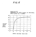
Fig. 6 is a graph of an output level (Pout) vs drain voltage (VDD4) characteristic obtained under the following conditions: VGG4 = 4.0 V, the frequency of the input signal is equal to 902.5 MHz, and the input level Pin thereof is equal to +5 dBm. It can be seen fromFig. 6 that the amplifier circuit shown inFig. 5 has a characteristic in which the output level Pout can be changed by 30 dBc by varying the drain voltage VDD4 between 4 V and 0 V. - On the other hand, according to the first amplifier circuit, the drain voltage of the
E-type MESFET 45 can be changed between 4 V and 0 V by varying the gate bias control voltage Vcontrol1 Further, the output level Pout can be varied over 30 dBc because the gate bias voltage VGB3A can be changed in the range of 0.4 V to 0 V. - When the amplifier circuit according to
Fig. 4 is made inactive, the gate bias control voltage Vcontrol1 is decreased to the lower limit, and the drain voltage of theE-type MESFET 45 and the gate bias voltage VGB3A are fixed to 0 V. Thus, it is possible to prevent the drain current from flowing in theE-type MESFET 45 even if the input signal IN is applied to the gate thereof. - As described above, according to the first amplifier circuit, only positive voltages such as the drain voltage VDD3 and the gate bias control voltage Vcontrol1, are used and any negative voltages are not needed, because only the E-type MESFET is used. Hence, it is necessary to provide only a positive power source, while a negative power source is not needed.
- Further, it is possible to greatly attenuate the input signal IN by changing the drain voltage of the
E-type MESFET 45 and the gate bias voltage VGB3A by changing the gate bias control voltage Vcontrol1 in the active state. In the inactive state, it is possible to prevent the drain current from flowing in theE-type MESFET 45 by decreasing the gate bias control voltage Vcontrol1 to the lower limit and then fixing the drain voltage of theE-type MESFET 45 and the gate bias voltage VGB3A to O V. Hence, it is not necessary to provide a switch element (switch module) directed to shutting the drain current between the drain voltage source and the drainvoltage input terminal 44. As a result, power consumption can be reduced nevertheless and a switch element is not required. - It is possible to omit the
resistor 50 provided between the gate bias controlvoltage input terminal 49 and the gate of theE-type MESFET 46. - A description will now be given, with reference to
Fig. 7 , of a second amplifier circuit which is useful for understanding the present invention. InFig. 7 , parts that are the same as those shown in the previously described figures are given the same reference numbers. In the amplifier circuit shown inFig. 7 , the source of theE-type MESFET 46 is coupled to the drain of theE-type MESFET 46 via aninductance element 67. The other portions of the amplifier circuit shown inFig. 7 are the same as those of the amplifier circuit according toFig. 4 .. - The
inductance element 67 functions to prevent the signal amplified by theE-type MESFET 45 from leaking to the side of the drain voltage source via theE-type MESFET 46. In the dc formation, the source of theE-type MESFET 46 is shortcircuited and connected to the drain of theE-type MESFET 45. - The second amplifier circuit has the same effects as those of the first amplifier circuit, and has an additional advantage in that the signal amplified by the
E-type MESFET 45 can be prevented from leaking to the drain voltage source via theE-type MESFET 46 and can be efficiently transferred to the next-stage circuit. - It is possible to omit the
resistor 50 provided between the gate bias controlvoltage input terminal 49 and the gate of theE-type MESFET 46. - A description will now be given, with reference to
Fig. 8 , of a third amplifier circuit. InFig. 8 , parts that are the same as those shown in the previously described figures are given the same reference numbers. According to the third amplifier circuit, the source of theE-type MESFET 46 is grounded via acapacitance element 68. The other circuit portions are the same as those of the circuit shown inFig. 7 . - The
capacitance element 68 causes signals having frequencies lower than the signal to be amplified by theE-type MESFET 45 and noise applied from the drain voltage source via the drainvoltage input terminal 44 to flow to the ground. - The third amplifier circuit thus configured has the advantages as those of the second amplifier circuit and an additional advantage in that signals having frequencies lower than the signal to be amplified by the
E-type MESFET 45 and noise applied from the drain voltage source via the drainvoltage input terminal 44 can be prevented from being transferred to the next-stage circuit. - It is possible to omit the
resistor 50 provided between the gate bias controlvoltage input terminal 49 and the gate of theE-type MESFET 46. - A description will now be given, with reference to
Fig. 9 , of a fourth amplifier circuit. InFig. 9 , parts that are the same as those shown in the previously described figures are given the same reference numbers. According to the fourth amplifier circuit, the source of theE-type MESFET 46 is coupled to the drain of theE-type MESFET 45 via aparallel resonation circuit 69. The other circuit portions of the circuit shown inFig. 9 are the same as those of the circuit according toFig. 4 . - The
parallel resonation circuit 69 is made up of an inductance element 70 and acapacitance element 71, and resonates at a frequency of the signal to be amplified by theE-type MESFET 45. - The fourth amplifier circuit has the same advantages as those of the first amplifier circuit and another advantage in that signals having frequencies other than the frequency of the signal to be amplified by the
E-type MESFET 45 can be prevented from being transferred to the next-stage circuit, so that the selectivity can be improved. - It is possible to omit the
resistor 50 provided between the gate bias controlvoltage input terminal 49 and the gate of theE-type MESFET 46. - A description will now be given, with reference to
Fig. 10 , of a fifth amplifier circuit. InFig. 10 , parts that are the same as those shown in the previously described figures are given the same reference numbers. The fifth amplifier circuit includes agate bias circuit 73 having a configuration different from that of thegate bias circuit 48 of tFig. 4. The other circuit portions are the same as those ofFig. 4 . - The
gate bias circuit 73 includes a gate bias source voltage input terminal 74, a gate bias controlvoltage input terminal 75, anE-type MESFET 76, andresistors voltage input terminal 75. The control voltage Vcontrol2 is a variable voltage for controlling the gate bias voltages VGB3A and VGB3B. TheE-type MESFET 76 controls the gate bias voltages VGB3A and VGB3B. - The fifth amplifier circuit is based on the assumption that the gate bias control voltage source which outputs the gate bias control voltage Vcontrol2 is not capable of generating 0 V and the lower limit of the voltage Vcontrol2 is equal to, for example, 0.2 V.
- The
E-type MESFET 76 has a drain connected to the gate bias source voltage input terminal 74, and a gate connected to the gate bias controlvoltage input terminal 75. Theresistors E-type MESFET 76 and the ground. Aconnection node 80 between theresistors E-type MESFET 46, and aconnection node 81 between theresistors 78 and 79 is connected to the gate of theE-type MESFET 45. - Thus, it is possible to control gain by varying the gate bias control voltage Vcontrol2 in the active state. For example, as the value of the gate bias control voltage Vcontrol2 is increased, the ON resistance of the
E-type MESFET 76 is decreased, and the current flowing in the resistors 77 - 79 is increased. Further, the gate bias voltage VGB3B of theE-type MESFET 46 is increased, and the ON resistance of theE type MESFET 46 is decreased. The drain voltage of theE-type MESFET 45 is increased and the gate bias voltage VGB3A is increased. As a result, the output level is increased. - As the value of the gate bias control voltage Vcontrol2 is decreased, the ON resistance of the
E-type MESFET 76 is increased, and the current flowing in the resistors 77 - 79 is decreased. Further, the gate bias voltage VGB3B of theE-type MESFET 46 is decreased, and the ON resistance of theE-type MESFET 46 is increased. The drain voltage of theE-type MESFET 45 is decreased, and the gate bias voltage VGB3A is decreased. Hence, the output level is decreased. - With the above in mind, the fifth amplifier circuit determines the value of the gate bias source voltage VGG3, the characteristics of the
E-type MESFETs resistors E-type MESFET 45 is changed between 4 V and 0 V, and the gate bias voltage VGB3A is changed between 0.4 V and 0 V. - When the amplifier circuit shown in
Fig. 10 is made inactive, the gate bias control voltage Vcontrol2 is decreased to the lower limit, and the drain voltage of theE-type MESFET 45 and the gate bias voltage VGB3A are fixed to O V. Hence, even if the input signal IN is applied to theE-type MESFET 45, the drain current cannot flow in theE-type MESFET 45. - As described above, according to the fifth amplifier circuit, only positive voltages such as the drain voltage VDD3, the gate bias source voltage VGG3 and the gate bias control voltage Vcontrol2, and any negative voltages are not needed, because only the E-type MESFETs are used. Hence, it is necessary to provide only a positive power source, while a negative power source is not needed.
- Further, it is possible to greatly attenuate the input signal IN by changing the drain voltage of the
E-type MESFET 45 and the gate bias voltage VGB3A by changing the gate bias control voltage Vcontrol2 in the active state. In the inactive state, it is possible to prevent the drain current from flowing in theE-type MESFET 45 by decreasing the gate bias control voltage Vcontrol2 to the lower limit and the fixing the drain voltage of theE-type MESFET 45 and the gate bias voltage VGB3A to 0 V. Hence, it is not necessary to provide a switch element (switch module) directed to shutting the drain current between the drain voltage source and the drainvoltage input terminal 44. As a result, power consumption can be reduced nevertheless and a switch element is not required. - It is possible to omit the
resistor 77 provided between the source of theE-type MESFET 76 and the gate thereof. - It is also possible to employ an inductance element provided between the source of the
E-type MESFET 46 and the drain of theE-type MESFET 45. In this case, it is possible to prevent the signal amplified by theE-type MESFET 45 from leaking to the drain voltage source via theE-type MESFET 46 and to efficiently transfer the signal amplified by theE-type MESFET 45 to the next-stage circuit. - It is also possible to employ, in addition to the above inductance element, a capacitance element connected between the source of the
E-type MESFET 46 and the ground. In this case, it is possible to obtain, in addition to the advantage resulting from the inductance element, an advantage in that signals having frequencies lower than the frequency of the signal to be amplified by theE-type MESFET 45 and noise from the drain voltage source can be prevented from being transferred to the next-stage circuit. - It is also possible to employ a parallel resonance circuit provided between the source of the
E-type MESFET 46 and the drain of theE-type MESFET 45. The parallel resonance circuit resonates at the frequency, of the signal to be amplified by theE-type MESFET 45, and prevents signals other than the desired signal from being transferred to the next-stage circuit. Hence, the selectivity can be improved. - A description will now be given, with reference to
Fig. 11 , of a sixth amplifier circuit. InFig. 11 , parts that are the same as those used in the first amplifier circuit are given the same reference numbers. The sixth amplifier circuit employs agate bias circuit 83 having a configuration different from that of thegate bias circuit 48 used inFig. 4 . The other parts are the same as those ofFig. 4 . - The
gate bias circuit 83 includes a gate bias source voltage input terminal 84, a gate bias controlvoltage input terminal 85, anE-type MESFET 86, andresistors voltage input terminal 85. The control voltage Vcontrol3 is a variable voltage for controlling the gate bias voltages VGB3A and VGB3B. TheE-type MESFET 86 controls the gate bias voltages VGB3A and VGB3B. - The sixth amplifier circuit is based on the assumption that the gate bias control voltage source which outputs the gate bias control voltage Vcontrol3is not capable of generating 0 V and the lower limit of the voltage Vcontrol3 is equal to, for example, 0.2 V.
- The drain of the
E-type MESFET 86 is connected to the gate bias source voltage input terminal 84, and the gate thereof is connected to the gate bias controlvoltage input terminal 85, which is connected to the gate of theE-type MESFET 46 via theresistor 87. Theresistors E-type MESFET 86 and the ground. Aconnection node 90 between theresistors E-type MESFET 45. - Thus, it is possible to control the gain by varying the gate bias control voltage Vcontrol3 in the active state. For example, as the value of the gate bias control voltage Vcontrol3 is increased, the gate bias VGB3B of the
E-type MESFET 46 is increased, and the ON resistance of theE-type MESFET 46 is decreased. Further, the drain voltage of theE-type MESFET 45 is increased and the ON resistance of theE-type MESFET 86 is decreased. The current flowing in theresistors - As the gate bias control voltage Vcontrol3 is decreased, the gate bias voltage VGB3B of the
E-type MESFET 46 is decreased, and the ON resistance of theE-type MESFET 46 is increased. Further, the drain voltage of theE-type MESFET 45 is decreased, and the ON resistance of theE-type MESFET 86 is increased. Hence, the current flowing in theresistors - With the above in mind, the sixth eamplifier circuit determines the value of the gate bias source voltage VGG3, the characteristics of the
E-type MESFE resistors E-type MESFET 45 is changed between 4 V and 0 V, and the gate bias voltage VGB3A is changed between 0.4 V and 0 V. - When the amplifier circuit shown in
Fig. 11 is made inactive, the gate bias control voltage Vcontrol3 is decreased to the lower limit, and the drain voltage of theE-type MESFET 45 and the gate bias voltage VGB3A are fixed to 0 V. Hence, even if the input signal IN is applied to theE-type MESFET 45, the drain current cannot flow in theE-type MESFET 45. - As described above, according to the sixth amplifier circuit, only positive voltages such as the drain voltage VDD3, the gate bias source voltage VGG3 and the gate bias control voltage Vcontrol3, and any negative voltages are not needed, because only the E-type MESFETs are used. Hence, it is necessary to provide only a positive power source, while a negative power source is not needed.
- Further, it is possible to greatly attenuate the input signal IN by changing the drain voltage of the
E-type MESFET 45 and the gate bias voltage VGB3A by changing the gate bias control voltage Vcontrol3 in the active state. In the inactive state, it is possible to prevent the drain current from flowing in theE-type MESFET 45 by decreasing the gate bias control voltage Vcontrol3 to the lower limit and the fixing the drain voltage of theE-type MESFET 45 and the gate bias voltage VGB3A to 0 V. Hence, it is not necessary to provide a switch element (switch module) directed to shutting the drain current between the drain voltage source and the drainvoltage input terminal 44. As a result, power consumption can be reduced nevertheless and a switch element is not required. - It is possible to omit the
resistor 87 provided between the gate bias controlvoltage input terminal 85 and theE-type MESFET 46. - It is also possible to employ an inductance element provided between the source of the
E-type MESFET 46 and the drain of theE-type MESFET 45. In this case, it is possible to prevent the signal amplified by theE-type MESFET 45 from leaking to the drain voltage source via theE-type MESFET 46 and to efficiently transfer the signal amplified by theE-type MESFET 45 to the next-stage circuit. - It is also possible to employ, in addition to the above inductance element, a capacitance element connected between the source of the
E-type MESFET 46 and the ground. In this case, it is possible to obtain, in addition to the advantage resulting from the inductance element, an advantage in that signals having frequencies lower than the frequency of the signal to be amplified by theE-type MESFET 45 and noise from the drain voltage source can be prevented from being transferred to the next-stage circuit. - It is also possible to employ a parallel resonance circuit provided between the source of the
E-type MESFET 46 and the drain of theE-type MESFET 45. The parallel resonance circuit resonates at the frequency of the signal to be amplified by theE-type MESFET 45, and prevents signals other than the desired signal from being transferred to the next-stage circuit. Hence, the selectivity can be improved. - A description will now be given, with reference to
Fig. 12 , of an amplifier circuit according to a first embodiment of the present invention. The amplifier circuit shown inFig. 12 includes asignal input terminal 92, asignal output terminal 93, a drainvoltage input terminal 94, an E-type MESFET functioning as an amplifying element, and acapacitance element 96 for DC isolation. A positive drain voltage VDD5 is applied to the drainvoltage input terminal 94. - The gate of the
E-type MESFET 95 is connected to thesignal input terminal 92, and the drain thereof is connected to the drainvoltage input terminal 94 and to thesignal output terminal 93 via thecapacitance element 96. - The amplifier circuit shown in
Fig. 12 includes agate bias circuit 97, which supplies the gate of theE-type MESFET 95 with a positive gate bias voltage VGB5. Thecircuit 97 includes a gate bias source voltage input terminal 98 via which a positive gate bias source voltage VGG5 is supplied. Thecircuit 97 has a gate bias controlvoltage input terminal 99, anE-type MESFET 100, andresistors E-type MESFET 100 controls the gate bias voltage VGB5. - The amplifier circuit shown in
Figure 12 is configured on the assumption that the gate bias control voltage source which outputs the gate bias control voltage Vcontrol4 is not capable of generating 0 V and the lower limit of the voltage Vcontrol4 is equal to, for example, 0.2 V. - The drain of the
E-type MESFET 100 is connected to the gate bias source voltage input terminal 98, and the gate thereof is connected to the bias controlvoltage input terminal 99. Theresistors E-type MESFET 100 and the ground. Aconnection node 103 between theresistors E-type MESFET 95. - According to the first embodiment of the present invention, it is possible to control the gain by varying the gate bias control voltage Vcontrol4 in the active state. For example, as the value of the gate bias control voltage Vcontrol4 is increased, the ON resistance of the
E-type MESFET 100 is decreased, and the current flowing in theresistors E-type MESFET 95 is increased, and the output level is increased. - As the value of the gate bias control voltage Vcontrol4 is reduced, the ON resistance of the
E-type MESFET 100 is increased, and the current flowing in theresistors E-type MESFET 95 is decreased, and the output level is reduced. - With the above in mind, the amplifier circuit of
Figure 12 determines the value of the gate bias source voltage VGG5, the characteristic of theE-type MESFET 100 and the resistance values of theresistors - When the amplifier circuit shown in
Fig. 12 is made inactive, the gate bias control voltage Vcontrol4 is set to 0.2 V. In this case, the gate bias voltage VGB5 can be set close to 0 V, and it is thus possible to set the drain current flowing in theE-type MESFET 95 equal to or lower than tens of microamperes. - In order to reduce the current flowing in the drain of the
E-type MESFET 95 to a value as small as possible in the inactive state, it is necessary to supply the gate of theE-type MESFET 95 with a voltage ch lower than the threshold voltage thereof, that a voltage as close to 0 V as possible. If the above cannot be performed, the drain current will be increased and the power consumption will also be increased. - Due to a limitation on the gate bias source which generates the gate bias source voltage VGG4, the gate bias source voltage VGG4 cannot be reduced until the gate bias voltage VGB4 is set equal to 0 V. In this case, it is impossible to reduce power consumption.
- According to the first embodiment of the present invention, even if the gate bias control voltage Vcontro14 cannot be set to 0 V, the gate bias voltage VGB5 can be made close to 0 V by setting the gate bias control voltage Vcontro14 equal to 0.2 V. Hence, it is possible to set the drain current flowing in the
E-type MESFET 95 equal to or lower than tens of microamperes and to thus reduce power consumption. - The inventors found that in the amplifier circuit shown in
Fig. 5 , a current IGG flowing in the gate of theE-type MESFET 59 in a saturated output operation is approximately twice or three times the current flowing when a D-type MESFET is used. For example, when theE-type MESFET 59 is a 3W-class transistor, the gate current IGG of 10 - 20 mA flows. Hence, there is a possibility that the gate bias VGB4 is decreased due to a voltage drop developing across the resistor 63 through which the gate current IGG4 flows. In this case, the circuit will shift to a state in which the output level is decreased. - If the
resistors 63 and 64 have sufficiently small values, a decrease in the gate bias voltage VGB4 can be suppressed even if the gate current IGG4 is large. However, if the resistance values of theresistors 63 and 64 are too small, a sufficient current cannot be supplied to theresistors 63 and 64 due to the current supply ability of the gate bias source. Even if the current supply ability of the gate bias source can be increased, a large current flows in theresistors 63 and 64 with the gate bias voltage VGB4 applied. Hence, power consumption cannot be reduced. - According to the first embodiment, the gate bias control voltage Vcontrol4 can be set equal to 0.2 V in the inactive state even if the resistance values of the
resistors E-type MESFET 95 is prevented. Hence, the current flowing in theresistors - Now, a case will be considered where the amplifier circuit shown in
Fig. 5 is used in the power amplifier of the transmit circuit of the portable telephone set, and an automatic power control voltage Vapc for controlling the transmit power is employed and applied to the gate bias sourcevoltage input terminal 62 instead of the gate bias source voltage VGG4. - Normally, the automatic power control voltage Vapc can be varied within a range of approximately 0.2 V to 2.5 V, and the upper limit of an automatic power control current Iapc is approximately equal to 5 mA. It is assumed that when the automatic power control voltage Vapc is equal to 2.5 V, the voltage applied across the gate and source of the
E-type MESFET 59 in operation is 0.5 V. In this case, it is required that the ratio of the resistance value of the resistor 63 to that of theresistor 64 is 4 : 1. - The minimum value of the sum of the resistance values of the
resistors 63 and 64 is obtained by Vapc-max/Iapc-max, and is equal to 500 Ω. Hence, the above sum becomes greater than 500 Ω, and the resistance value of the resistor 63 is greater than 400 n. - With the above in mind, when the tolerable variation value of the voltage between the gate and source of the
E-type MESFET 59 is set equal to, for example, 0.1 V, the current IGG4 flowing to the gate of theE-type MESFET 59 is determined as follows. The value obtained by (the resistance value of the resistor 63) x IGG4 is less than 0.1 V. Hence, IGG4 is less than (0.1 V /400 Ω), namely, 0.25 mA. In terms of the above, if the current IGG4 flowing in the gate and source of theE-type MESFET 59 is equal to or greater than 0.5 mA, the tolerable variation value of the voltage between the gate and source of theE-type MESFET 59 exceeds 0.1 V. In this case, the configuration according toFigure 12 is required. - The first embodiment of the present invention employs only the E-type MESFETs, and thus the drain voltage VDD5, the gate bias source voltage VGG5 and the gate bias control voltage Vcontrol4 are positive voltages, which can be produced by a positive power source. That is, no negative power source is needed.
- In the active state, it is possible to control the gain by varying the gate bias control voltage Vcontro14 and thus changing the gate bias voltage VGB5 of the
E-type MESFET 95. - In the inactive state, it is possible to prevent the drain current from flowing in the
E-type MESFET 95 by decreasing the gate bias control voltage Vcontrol4 to the lower limit and setting the gate bias voltage VGB5 of theE-type MESFET 95 close to 0 V. Hence, it is possible to reduce power consumption without any switch element (switch module) directed to shutting the drain current between the drain voltage source and the drainvoltage input terminal 94. - It is possible to omit the
resistor 101 between the source of theE-type MESFET 100 and the gate of theE-type MESFET 95. - A description will now be given of a multistage amplifier circuit according to a second embodiment of the present invention.
-
Fig. 13 is a circuit diagram of a multistage amplifier circuit according to the second embodiment of the present invention, which is applied to the power amplifier of the transmit circuit part of the portable telephone set. The input signal (high frequency signal) IN is applied to asignal input terminal 106. An output signal (high frequency signal) OUT is output via a signal output terminal OUT. Acapacitance element 108 prevents a DC component from DC isolation. There are provided threeamplifier circuits voltage generating circuit 112 generates a gate bias control voltage vcontro15 to be supplied to theamplifier circuits - The
circuit 112 is configured as follows. The automatic power control voltage Vapc is applied to an automatic power controlvoltage input terminal 113. The voltage Vapc serves as a control signal which automatically controls the output level of the output signal OUT supplied from a control circuit part (not shown) of the portable telephone set. Thecircuit 112 includes tworesistors connection node 116 between theresistors control voltage line 117 is connected to theconnection node 116. - The
amplifier circuit 109 is configured as follows. A positive drain voltage VDD6 is applied to a drainvoltage input terminal 118. AnE-type MESFET 119 functions as an amplifying element. AnE-type MESFET 120 controls the drain voltage of theE-type MESFET 119. Acapacitance element 121 is used for DC isolation. Aninductance element 122 is provided between the source of theE-type MESFET 120 and the drain of theE-type MESFET 119. - The gate of the
E-type MESFET 119 is connected to thesignal input terminal 106 via thecapacitance element 108, and the drain thereof is connected to the source of theE-type MESFET 120 via theinductance element 122 and to one end of thecapacitance element 121. The source of theE-type MESFET 119 is grounded. The drain of theE-type MESFET 120 is connected to the drainvoltage input terminal 118. - The
amplifier circuit 109 includes agate bias circuit 123, which supplies positive gate bias voltages VGB6A and VGB6B to the gates of theE-type MESFETS circuit 123 includesresistors resistors control voltage line 117 and the ground. Aconnection node 127 between theresistors E-type MESFET 120. Aconnection node 128 between theresistors E-type MESFET 119. - The
amplifier circuit 110 is configured as follows. The positive drain voltage VDD6 is applied to a drain voltage input terminal 129. AnE-type MESFET 130 functions as an amplifying element. Acapacitance element 131 is used for DC isolation. The gate of theE-type MESFET 130 is connected to the other end of thecapacitance element 121, and the drain thereof is connected to the drain voltage input terminal 129 and one end of thecapacitance element 131. - The
amplifier circuit 110 includes agate bias circuit 132, which supplies a positive gate bias voltage VGB6C to the gate of theE-type MESFET 130. Thecircuit 132 has a gate bias source voltage input terminal to which the positive gate bias source voltage VGG6 is applied. Thecircuit 132 includes anE-type MESFET 134, which controls the gate bias voltage VGB6C, andresistors E-type MESFET 134 is connected to the gate bias sourcevoltage input terminal 133, and the gate thereof is connected to the gatebias voltage line 117 via aresistor 138. Theresistor 138 attenuates the signal output to the gate of theE-type MESFET 134 in order to prevent occurrence of oscillation. If the signal amplified by theE-type MESFET 119 is fed back to theamplifier circuit 109 via thecapacitance element 121, theresistor 135 and the source and gate of theE-type MESFET 134, the circuit may oscillate. - The
resistors E-type MESFET 134 and the ground. A connection node 137 between theresistors E-type MESFET 130. - The amplifier circuit 111 has a drain voltage input terminal 139 to which the positive drain voltage VDD6 is applied, an
E-type MESFET 140 functioning as an amplifying element, and acapacitance element 141 for DC isolation. The gate of theE-type MESFET 140 is connected to the other end of thecapacitance element 131, and the drain thereof is connected to the drain voltage input terminal 139 and to thesignal output terminal 107 via thecapacitance element 141. The source of theE-type MESFET 140 is grounded. - The amplifier circuit 111 includes a
gate bias circuit 142, which supplies a positive gate bias voltage VGB6D to the gate of theE-type MESFET 140. Thecircuit 142 includes a gate bias sourcevoltage input terminal 143, to which the positive gate bias source voltage VGG6 is applied. Thecircuit 142 includes anE-type MESFET 144 for controlling the gate bias voltage VGB6B, andresistors E-type MESFET 144 is connected to the gate bias sourcevoltage input terminal 143, and the gate thereof is connected to the gatebias voltage line 117 via aresistor 147. Theresistor 147 attenuates the signal output to the gate of theE-type MESFET 134 in order to prevent occurrence of oscillation. If the signal amplified by theE-type MESFET 130 is fed back to theamplifier circuits capacitance element 131, theresistor 145 and the source and gate of theE-type MESFET 144 may oscillate. - The
resistors E-type MESFET 144 and the ground. Aconnection node 148 between theresistors E-type MESFET 140. - It will be noted that the
first amplifier circuit 109 has the same configuration as that of the second embodiment of the present invention, and theamplifier circuits 110 and 111 of the second and third stages have the same configuration as that of the first embodiment of the present invention. - According to the multistage amplifier circuit of the second embodiment of the present invention thus configured, it is possible to provide, as the automatic power control voltage Vapc, the voltage necessary to obtain the transmit output determined by the positional relationship (distance) between the portable telephone set and a ground station.
-
Fig. 14 is a diagram explaining ranges of variations in the output levels of theamplifier circuits -
Fig. 14 denotes the positions of the output terminals of theamplifier circuits Fig. 14 , anarrow 151 indicates a variation range of the output level of theamplifier circuit 109. Anarrow 152 indicates a variation range of the output level of theamplifier circuit 110. Anarrow 153 indicates a variation range of the output level of the amplifier 111, that is, the output signal OUT. - As is known, if the portable telephone set is close to the ground station, a signal received in the ground station will be distorted unless the transmit power is reduced according to the distance between the portable telephone set and the ground station. Hence, an instruction to reduce the transmit power is sent to the portable telephone set from the ground station. In response to this instruction, the automatic power control voltage Vapc is varied. It is required to have a variable range of the transmit output equal to 60 dBc.
- In a case where the
amplifier circuits 110 and 111 of the second and third stages are configured as shown inFig. 13 , it is necessary to set the variable range of the output level of the first-stage amplifier circuit 109 to be as large as 30 dBc in order to obtain a variable range of the output signal OUT of 60 dBc. Theamplifier circuit 109 of the first stage has the same configuration as thatFig. 7 . Thus, it is possible to vary the output level over 30 dBc and greatly attenuate the input signal IN. - It may be possible to use the first-
stage amplifier circuit 109 having the structure shown inFig. 5 . The input/output characteristic of the amplifier circuit shown inFig. 5 is as shown inFig. 15 . InFig. 15 , asolid line 155 indicates a case where the gate bias voltage VGB4 of theE-type MESFET 59 is 0.4 V, and abroken line 156 indicates a case where the gate bias voltage VGB4 of theE-type MESFET 59 is 0.0 V. It can be seen from the graph ofFig. 15 that it is possible to obtain only the range of a variation in the output level Pout equal to 20 dBc by controlling the gate bias voltage VGB4 even if the input level Pin is decreased by 20 dB from the saturation level. Hence, it is impossible to greatly attenuate the input signal IN. - If the input level Pin can be varied, the variable range of the output level Pout can be set greater than 20 dBc. In practice, it is usually required that the power amplifier of the portable telephone set employs the fixed input level Pin in order to make the structure as simple as possible and reduce the production cost. In this regard, the amplifier circuit shown in
Fig. 5 is not suitable for theamplifier circuit 109 of the first stage. - In the multistage amplifier circuit shown in
Fig. 13 , the automatic power control voltage Vapc equal to 0.2 V is supplied when the portable telephone set is receiving a signal or waiting for receipt of a signal. Hence, the gate bias voltage VGB6B of theE-type MESFET 120 in theamplifier circuit 109 is decreased, and the drain voltage of theE-type MESFET 119 can be set equal to 0 V. Further, the gate bias voltage VGB6A of theE-type MESFET 119 can be decreased close to 0 V. Hence, the drain current does not flow in theE-type MESFET 119. - The gate voltage of the
E-type MESFET 134 in theamplifier circuit 110 is decreased, so that the gate bias voltage VGB6C of theE-type MESFET 130 can be set close to 0 V. As a result, it is possible to reduce the drain current flowing in theE-type MESFET 130 to a very small value. - The gate voltage of the
E-type MESFET 144 in the amplifier circuit 111 is decreased, so that the gate bias voltage VGB6D of theE-type MESFET 140 can be set close to 0 V. As a result, it is possible to reduce the drain current flowing in theE-type MESFET 140 to a very small value. - As described above, the second embodiment of the present invention employs only the E-type MESFETs which operate with the positive voltages, and thus use only the positive drain voltage VDD6, the positive gate bias source voltage VGG6 and the positive automatic power control voltage Vapc. In other words, the second embodiment of the present invention does not require any negative voltages. Hence, it is possible to realize cost reduction and down sizing for the portable telephone sets.
- The first-
stage amplifier circuit 109 has the same structure as that ofFig.7 . - Hence, it is possible to obtain the variable range of the output level of the first-
stage amplifier circuit 109 over 30 dBc and thus obtain the variable range of the output level of the final-stage amplifier circuit 111 over 60 dBc. As a result, it is possible to satisfy the transmit output variable range required for the portable telephone sets. - The second-
stage amplifier circuit 110 has the same structure as that of the first embodiment of the present invention shown inFig. 12 . Hence,it is possible to reduce the current flowing in theresistors E-type MESFET 134 at the time of receiving and waiting for a signal even if theresistors E-type MESFET 130. Hence, it is possible to reduce power consumption. - The third-stage amplifier circuit 111 has the same structure as that of the first embodiment of the present invention. Hence,it is possible to reduce the current flowing in the
resistors E-type MESFET 144 at the time of receiving and waiting for a signal even if theresistors E-type MESFET 140. Hence, it is possible to reduce power consumption. - At the time of receiving or waiting for a signal, the drain current does not flow in the
E-type MESFET 119 and very small drain currents flow in theE-type MESFETs E-type MESFETs - The
amplifier circuit 109 of the first stage can be configured so as to have the same configuration as any of the first to sixth, amplifier circuits described above. - It is possible to omit the
resistors voltage input terminal 113 and the ground. In this case, the terminal 113 is directly connected to the gate biascontrol voltage line 117. It is also possible to omit theresistor 124 between the gate biascontrol voltage line 117 and the gate of theE-type MESFET 120. It is also possible to omit theresistor 135 provided between the source of theE-type MESFET 134 and the gate of theE-type MESFET 130 as well as theresistor 145 provided between the source of theE-type MESFET 144 and the gate of theE-type MESFET 140. - It is also possible to omit the
resistor 138 provided between the gate of theE-type MESFET 134 and the gate biascontrol voltage line 117 and theresistor 144 provided between the gate of theE-type MESFET 144 and theline 117. - The MESFETs used in the present invention are, for example, MESFETs using compound semiconductor elements.
- The present invention is not limited to the specifically disclosed embodiments, and variations and modifications may be made without departing from the scope of the present invention.
Claims (8)
- An amplifier circuit comprising:a first FET (95) of an enhancement type having a source, a gate supplied with an input signal (IN) and a gate bias voltage (VGB5), and a drain via which an amplified output signal (OUT) is output, thereby forming a current path directed to the source from the gate;a second FET (100) of the enhancement type having a drain connected to a gate bias supply source for the first FET (95), a gate supplied with a control signal (Vcontrol4), and a source via which a source voltage controlled by the control signal is output, the source voltage being supplied to the gate of the first FET (95) as the gate bias voltage; anda resistance element (102) having a first end connected to the source of the second FET (100) and the gate of the first FET (95), and having a second end grounded;characterized in that:said amplifier circuit requires only a positive power source.
- The amplifier circuit as claimed in claim 1,
wherein the gate of the first FET (95) is supplied, as the gate bias voltage (VGB5), with a voltage obtained by dividing the source voltage of the second FET (100) by resistors (101, 102). - A multistage amplifier circuit comprising:a first-stage amplifier circuit (109) amplifying an input signal; anda second-stage amplifier circuit (110, 111) including a first FET (130, 140) of an enhancement type having a source, a gate supplied with an input signal and a gate bias voltage (VGB6C, VGB6D), and a drain via which an amplified output signal (OUT) is output, thereby forming a current path directed to the source from the gate, and a second FET (134, 144) of the enhancement type having a drain connected to a gate bias supply source for the first FET (130, 140), a gate supplied with a control signal (Vcontrol5), and a source via which a source voltage controlled by the control signal is output, the source voltage being supplied to the gate of the first FET (130, 140) as the gate bias voltage; anda resistance element (136, 146) having a first end connected to the source of the second FET (134, 144) and the gate of the first FET (130, 140), and having a second end grounded;wherein said second-stage amplifier circuit requires only a positive power source.
- The multistage amplifier circuit as claimed in claim 3, further comprising a capacitance element (121) provided between the first-stage amplifier circuit (109) and the second-stage amplifier circuit (110, 111).
- The multistage amplifier as claimed in claim 4,
wherein another control signal for controlling a gain of the second-stage amplifier circuit is applied to the second-stage amplifier circuit (110, 111). - The multistage amplifier circuit as claimed in claim 5, wherein the control signal (Vcontrol5) supplied to the gate of the second FET (134, 144) and said another control signal are provided as a common signal.
- The multistage amplifier circuit as claimed in claim 6, further comprising an impedance element (138, 147) provided between the gate of the second FET (134, 144) and an input terminal of the second-stage amplifier circuit (110, 111) to which the common signal is applied.
- An amplifier circuit as claimed in claim 1 or 2, or a multistage amplifier circuit as claimed in any of claims 3 to 7, wherein the first and second FETs (95, 100; 130, 140; 134, 144) are MESFETs using compound semiconductor elements.
Applications Claiming Priority (3)
| Application Number | Priority Date | Filing Date | Title |
|---|---|---|---|
| JP18291596 | 1996-07-12 | ||
| JP18291596A JP3508401B2 (en) | 1996-07-12 | 1996-07-12 | Amplifier circuit and multi-stage amplifier circuit |
| EP97301156A EP0818879B1 (en) | 1996-07-12 | 1997-02-21 | Amplifier circuit and multistage amplifier circuit |
Related Parent Applications (1)
| Application Number | Title | Priority Date | Filing Date |
|---|---|---|---|
| EP97301156A Division EP0818879B1 (en) | 1996-07-12 | 1997-02-21 | Amplifier circuit and multistage amplifier circuit |
Publications (3)
| Publication Number | Publication Date |
|---|---|
| EP1387486A2 EP1387486A2 (en) | 2004-02-04 |
| EP1387486A3 EP1387486A3 (en) | 2005-11-23 |
| EP1387486B1 true EP1387486B1 (en) | 2008-08-06 |
Family
ID=16126617
Family Applications (2)
| Application Number | Title | Priority Date | Filing Date |
|---|---|---|---|
| EP97301156A Expired - Lifetime EP0818879B1 (en) | 1996-07-12 | 1997-02-21 | Amplifier circuit and multistage amplifier circuit |
| EP03014428A Expired - Lifetime EP1387486B1 (en) | 1996-07-12 | 1997-02-21 | Amplifier circuit and multistage amplifier circuit |
Family Applications Before (1)
| Application Number | Title | Priority Date | Filing Date |
|---|---|---|---|
| EP97301156A Expired - Lifetime EP0818879B1 (en) | 1996-07-12 | 1997-02-21 | Amplifier circuit and multistage amplifier circuit |
Country Status (7)
| Country | Link |
|---|---|
| US (1) | US5994963A (en) |
| EP (2) | EP0818879B1 (en) |
| JP (1) | JP3508401B2 (en) |
| KR (1) | KR100302685B1 (en) |
| CN (1) | CN1090839C (en) |
| DE (2) | DE69726058T2 (en) |
| TW (1) | TW325606B (en) |
Families Citing this family (26)
| Publication number | Priority date | Publication date | Assignee | Title |
|---|---|---|---|---|
| FR2763183A1 (en) * | 1997-05-07 | 1998-11-13 | Philips Electronics Nv | DEVICE INCLUDING A BROADBAND AMPLIFIER CIRCUIT |
| JP2000223960A (en) * | 1999-02-01 | 2000-08-11 | Fujitsu Ltd | Distortion compensator |
| US6097253A (en) * | 1999-02-12 | 2000-08-01 | Pmc-Sierra Ltd. | High speed process-controlled transresistance amplifier |
| EP1279046B1 (en) * | 2000-04-07 | 2007-04-04 | The Chief Controller, Research and Development, Defence Research and Development Organisation of Ministry of Defence | Transmit/receiver module for active phased array antenna |
| US6549071B1 (en) * | 2000-09-12 | 2003-04-15 | Silicon Laboratories, Inc. | Power amplifier circuitry and method using an inductance coupled to power amplifier switching devices |
| US6323731B1 (en) * | 2000-10-06 | 2001-11-27 | Tropion, Inc. Corp. | Variable bias control for switch mode RF amplifier |
| JP2002151982A (en) | 2000-11-15 | 2002-05-24 | Hitachi Ltd | High frequency power amplifier circuit, wireless communication device, and wireless communication system |
| DE10123395A1 (en) * | 2001-05-14 | 2002-11-28 | Infineon Technologies Ag | Circuit arrangement with cascaded field effect transistors |
| US6701138B2 (en) * | 2001-06-11 | 2004-03-02 | Rf Micro Devices, Inc. | Power amplifier control |
| US6647172B2 (en) | 2001-06-29 | 2003-11-11 | Lucent Technologies Inc. | Imaging technique for use with optical MEMS devices |
| JP2003037454A (en) | 2001-07-23 | 2003-02-07 | Hitachi Ltd | High frequency power amplifier circuit |
| US6724252B2 (en) * | 2002-02-21 | 2004-04-20 | Rf Micro Devices, Inc. | Switched gain amplifier circuit |
| US6701134B1 (en) | 2002-11-05 | 2004-03-02 | Rf Micro Devices, Inc. | Increased dynamic range for power amplifiers used with polar modulation |
| US7177370B2 (en) | 2003-12-17 | 2007-02-13 | Triquint Semiconductor, Inc. | Method and architecture for dual-mode linear and saturated power amplifier operation |
| US7109791B1 (en) | 2004-07-09 | 2006-09-19 | Rf Micro Devices, Inc. | Tailored collector voltage to minimize variation in AM to PM distortion in a power amplifier |
| JP4583967B2 (en) * | 2005-02-23 | 2010-11-17 | パナソニック株式会社 | High frequency power amplifier and output power adjustment method thereof |
| JP4650026B2 (en) * | 2005-03-01 | 2011-03-16 | 日本電気株式会社 | Power amplifier |
| US7336127B2 (en) * | 2005-06-10 | 2008-02-26 | Rf Micro Devices, Inc. | Doherty amplifier configuration for a collector controlled power amplifier |
| US7330071B1 (en) | 2005-10-19 | 2008-02-12 | Rf Micro Devices, Inc. | High efficiency radio frequency power amplifier having an extended dynamic range |
| EP2045915A1 (en) * | 2007-10-03 | 2009-04-08 | Seiko Epson Corporation | Low noise amplifier and mixer front-end circuit and method for gain control |
| FR2942681B1 (en) * | 2009-02-27 | 2011-05-13 | Commissariat Energie Atomique | MICROMETRIC OR NANOMETRIC RESONANT DEVICE WITH TRANSISTORS |
| US8666339B2 (en) * | 2012-03-29 | 2014-03-04 | Triquint Semiconductor, Inc. | Radio frequency power amplifier with low dynamic error vector magnitude |
| DE102015107655B4 (en) * | 2015-05-15 | 2019-06-13 | Brandenburgische Technische Universität Cottbus-Senftenberg | Electric signal amplifier, circuit arrangement and method for amplifying an electrical signal |
| CN110365207B (en) * | 2018-04-10 | 2020-10-09 | 中芯国际集成电路制造(上海)有限公司 | Amplifying circuit |
| US10769511B2 (en) | 2019-01-03 | 2020-09-08 | Wiliot, Ltd | Low energy transmitter |
| WO2023150714A2 (en) * | 2022-02-04 | 2023-08-10 | ChargeStar, Inc. | High voltage multipliers |
Family Cites Families (11)
| Publication number | Priority date | Publication date | Assignee | Title |
|---|---|---|---|---|
| US4015219A (en) * | 1974-01-16 | 1977-03-29 | Hitachi, Ltd. | Electronic circuit using field effect transistor with compensation means |
| US3913026A (en) * | 1974-04-08 | 1975-10-14 | Bulova Watch Co Inc | Mos transistor gain block |
| US4255716A (en) * | 1977-09-10 | 1981-03-10 | Tokyo Shibaura Denki Kabushiki Kaisha | Automatic gain control circuit |
| FR2558659B1 (en) * | 1984-01-20 | 1986-04-25 | Thomson Csf | POLARIZATION CIRCUIT OF A FIELD EFFECT TRANSISTOR |
| US4672327A (en) * | 1986-03-10 | 1987-06-09 | Rca Corporation | Self-biasing for enhancement-mode field effect transistors |
| US4701646A (en) * | 1986-11-18 | 1987-10-20 | Northern Telecom Limited | Direct coupled FET logic using a photodiode for biasing or level-shifting |
| FR2623951B1 (en) * | 1987-11-27 | 1990-03-09 | Thomson Hybrides Microondes | VERY WIDE BROADBAND MICROWAVE LINEAR AMPLIFIER |
| DE3814041A1 (en) * | 1988-04-26 | 1989-11-09 | Standard Elektrik Lorenz Ag | CONTROLLABLE AC VOLTAGE AMPLIFIER |
| TW198152B (en) * | 1990-10-18 | 1993-01-11 | Hitachi Seisakusyo Kk | |
| JPH05267585A (en) * | 1992-03-19 | 1993-10-15 | Mitsubishi Electric Corp | amplifier |
| JPH0851318A (en) * | 1994-08-08 | 1996-02-20 | Oki Electric Ind Co Ltd | Variable gain circuit and its integrated circuit |
-
1996
- 1996-07-12 JP JP18291596A patent/JP3508401B2/en not_active Expired - Fee Related
-
1997
- 1997-02-21 DE DE69726058T patent/DE69726058T2/en not_active Expired - Lifetime
- 1997-02-21 EP EP97301156A patent/EP0818879B1/en not_active Expired - Lifetime
- 1997-02-21 DE DE69738890T patent/DE69738890D1/en not_active Expired - Lifetime
- 1997-02-21 EP EP03014428A patent/EP1387486B1/en not_active Expired - Lifetime
- 1997-02-24 US US08/804,042 patent/US5994963A/en not_active Expired - Lifetime
- 1997-03-04 TW TW086102591A patent/TW325606B/en not_active IP Right Cessation
- 1997-03-12 KR KR1019970008187A patent/KR100302685B1/en not_active Expired - Fee Related
- 1997-03-13 CN CN97103122A patent/CN1090839C/en not_active Expired - Fee Related
Also Published As
| Publication number | Publication date |
|---|---|
| CN1090839C (en) | 2002-09-11 |
| EP1387486A2 (en) | 2004-02-04 |
| JPH1028020A (en) | 1998-01-27 |
| DE69738890D1 (en) | 2008-09-18 |
| EP1387486A3 (en) | 2005-11-23 |
| TW325606B (en) | 1998-01-21 |
| US5994963A (en) | 1999-11-30 |
| KR980012845A (en) | 1998-04-30 |
| DE69726058T2 (en) | 2004-08-26 |
| CN1170988A (en) | 1998-01-21 |
| EP0818879A3 (en) | 1999-04-07 |
| KR100302685B1 (en) | 2001-09-22 |
| EP0818879B1 (en) | 2003-11-12 |
| JP3508401B2 (en) | 2004-03-22 |
| EP0818879A2 (en) | 1998-01-14 |
| DE69726058D1 (en) | 2003-12-18 |
Similar Documents
| Publication | Publication Date | Title |
|---|---|---|
| US5994963A (en) | Amplifier circuit and multistage amplifier circuit | |
| KR100305917B1 (en) | Semiconductor Power Amplifier Integrated Circuit | |
| US6215355B1 (en) | Constant impedance for switchable amplifier with power control | |
| US6492872B1 (en) | High frequency power amplifying module and wireless communication apparatus | |
| JP2005518684A (en) | Power amplifier control | |
| US6351188B1 (en) | Variable gain amplifier circuit and gain control method | |
| EP0998033A1 (en) | Semiconductor circuit | |
| US6624700B2 (en) | Radio frequency power amplifier for cellular telephones | |
| US5748042A (en) | Method for altering a difference frequency signal and amplifier circuit thereof | |
| US6265942B1 (en) | Low power gain controlled amplifier with high dynamic range | |
| US5345123A (en) | Attenuator circuit operating with single point control | |
| JP2008516510A (en) | Dual bias control circuit | |
| CA2008594C (en) | Transmitter using gallium arsenide fet with means for controlling gate bias voltage of the fet for suppressing undesired signal at a start condition of the transmitter | |
| EP0622895B1 (en) | Communication apparatus utilizing power amplifier | |
| US6999740B2 (en) | Semiconductor integrated circuit and radio communication apparatus using same | |
| EP1153475B1 (en) | Gate biasing arrangement | |
| US6052030A (en) | Low voltage variable gain amplifier with feedback | |
| US6188283B1 (en) | Amplifier and semiconductor device therefor | |
| US6100763A (en) | Circuit for RF buffer and method of operation | |
| US6445729B1 (en) | Radio signal transceiver apparatus | |
| US5751181A (en) | Power amplifier circuit | |
| US6693492B2 (en) | Variable gain low-noise amplifier and method | |
| JP3983511B2 (en) | Variable gain amplifier circuit and receiver and transmitter using the same | |
| JP3108712U (en) | Variable gain amplifier circuit | |
| JP2008011482A (en) | High-frequency circuit |
Legal Events
| Date | Code | Title | Description |
|---|---|---|---|
| PUAI | Public reference made under article 153(3) epc to a published international application that has entered the european phase |
Free format text: ORIGINAL CODE: 0009012 |
|
| AC | Divisional application: reference to earlier application |
Ref document number: 0818879 Country of ref document: EP Kind code of ref document: P |
|
| AK | Designated contracting states |
Kind code of ref document: A2 Designated state(s): DE FR GB |
|
| PUAL | Search report despatched |
Free format text: ORIGINAL CODE: 0009013 |
|
| AK | Designated contracting states |
Kind code of ref document: A3 Designated state(s): DE FR GB |
|
| 17P | Request for examination filed |
Effective date: 20060322 |
|
| AKX | Designation fees paid |
Designated state(s): DE FR GB |
|
| 17Q | First examination report despatched |
Effective date: 20060911 |
|
| GRAP | Despatch of communication of intention to grant a patent |
Free format text: ORIGINAL CODE: EPIDOSNIGR1 |
|
| GRAS | Grant fee paid |
Free format text: ORIGINAL CODE: EPIDOSNIGR3 |
|
| GRAA | (expected) grant |
Free format text: ORIGINAL CODE: 0009210 |
|
| AC | Divisional application: reference to earlier application |
Ref document number: 0818879 Country of ref document: EP Kind code of ref document: P |
|
| AK | Designated contracting states |
Kind code of ref document: B1 Designated state(s): DE FR GB |
|
| REG | Reference to a national code |
Ref country code: GB Ref legal event code: FG4D |
|
| REF | Corresponds to: |
Ref document number: 69738890 Country of ref document: DE Date of ref document: 20080918 Kind code of ref document: P |
|
| PLBE | No opposition filed within time limit |
Free format text: ORIGINAL CODE: 0009261 |
|
| STAA | Information on the status of an ep patent application or granted ep patent |
Free format text: STATUS: NO OPPOSITION FILED WITHIN TIME LIMIT |
|
| 26N | No opposition filed |
Effective date: 20090507 |
|
| PGFP | Annual fee paid to national office [announced via postgrant information from national office to epo] |
Ref country code: FR Payment date: 20120221 Year of fee payment: 16 |
|
| PGFP | Annual fee paid to national office [announced via postgrant information from national office to epo] |
Ref country code: DE Payment date: 20120215 Year of fee payment: 16 |
|
| PGFP | Annual fee paid to national office [announced via postgrant information from national office to epo] |
Ref country code: GB Payment date: 20120215 Year of fee payment: 16 |
|
| GBPC | Gb: european patent ceased through non-payment of renewal fee |
Effective date: 20130221 |
|
| REG | Reference to a national code |
Ref country code: FR Ref legal event code: ST Effective date: 20131031 |
|
| REG | Reference to a national code |
Ref country code: DE Ref legal event code: R119 Ref document number: 69738890 Country of ref document: DE Effective date: 20130903 |
|
| PG25 | Lapsed in a contracting state [announced via postgrant information from national office to epo] |
Ref country code: DE Free format text: LAPSE BECAUSE OF NON-PAYMENT OF DUE FEES Effective date: 20130903 Ref country code: GB Free format text: LAPSE BECAUSE OF NON-PAYMENT OF DUE FEES Effective date: 20130221 Ref country code: FR Free format text: LAPSE BECAUSE OF NON-PAYMENT OF DUE FEES Effective date: 20130228 |