EP1387225A1 - Image forming apparatus with a cleaning brush - Google Patents
Image forming apparatus with a cleaning brush Download PDFInfo
- Publication number
- EP1387225A1 EP1387225A1 EP03017100A EP03017100A EP1387225A1 EP 1387225 A1 EP1387225 A1 EP 1387225A1 EP 03017100 A EP03017100 A EP 03017100A EP 03017100 A EP03017100 A EP 03017100A EP 1387225 A1 EP1387225 A1 EP 1387225A1
- Authority
- EP
- European Patent Office
- Prior art keywords
- photoreceptor
- image
- forming apparatus
- toner
- protection layer
- Prior art date
- Legal status (The legal status is an assumption and is not a legal conclusion. Google has not performed a legal analysis and makes no representation as to the accuracy of the status listed.)
- Withdrawn
Links
Images




Classifications
-
- G—PHYSICS
- G03—PHOTOGRAPHY; CINEMATOGRAPHY; ANALOGOUS TECHNIQUES USING WAVES OTHER THAN OPTICAL WAVES; ELECTROGRAPHY; HOLOGRAPHY
- G03G—ELECTROGRAPHY; ELECTROPHOTOGRAPHY; MAGNETOGRAPHY
- G03G5/00—Recording-members for original recording by exposure, e.g. to light, to heat or to electrons; Manufacture thereof; Selection of materials therefor
- G03G5/14—Inert intermediate or cover layers for charge-receiving layers
- G03G5/147—Cover layers
- G03G5/14704—Cover layers comprising inorganic material
-
- G—PHYSICS
- G03—PHOTOGRAPHY; CINEMATOGRAPHY; ANALOGOUS TECHNIQUES USING WAVES OTHER THAN OPTICAL WAVES; ELECTROGRAPHY; HOLOGRAPHY
- G03G—ELECTROGRAPHY; ELECTROPHOTOGRAPHY; MAGNETOGRAPHY
- G03G21/00—Arrangements not provided for by groups G03G13/00 - G03G19/00, e.g. cleaning, elimination of residual charge
- G03G21/0005—Arrangements not provided for by groups G03G13/00 - G03G19/00, e.g. cleaning, elimination of residual charge for removing solid developer or debris from the electrographic recording medium
- G03G21/0035—Arrangements not provided for by groups G03G13/00 - G03G19/00, e.g. cleaning, elimination of residual charge for removing solid developer or debris from the electrographic recording medium using a brush; Details of cleaning brushes, e.g. fibre density
-
- G—PHYSICS
- G03—PHOTOGRAPHY; CINEMATOGRAPHY; ANALOGOUS TECHNIQUES USING WAVES OTHER THAN OPTICAL WAVES; ELECTROGRAPHY; HOLOGRAPHY
- G03G—ELECTROGRAPHY; ELECTROPHOTOGRAPHY; MAGNETOGRAPHY
- G03G5/00—Recording-members for original recording by exposure, e.g. to light, to heat or to electrons; Manufacture thereof; Selection of materials therefor
- G03G5/02—Charge-receiving layers
- G03G5/04—Photoconductive layers; Charge-generation layers or charge-transporting layers; Additives therefor; Binders therefor
- G03G5/05—Organic bonding materials; Methods for coating a substrate with a photoconductive layer; Inert supplements for use in photoconductive layers
- G03G5/0503—Inert supplements
- G03G5/0507—Inorganic compounds
-
- G—PHYSICS
- G03—PHOTOGRAPHY; CINEMATOGRAPHY; ANALOGOUS TECHNIQUES USING WAVES OTHER THAN OPTICAL WAVES; ELECTROGRAPHY; HOLOGRAPHY
- G03G—ELECTROGRAPHY; ELECTROPHOTOGRAPHY; MAGNETOGRAPHY
- G03G21/00—Arrangements not provided for by groups G03G13/00 - G03G19/00, e.g. cleaning, elimination of residual charge
- G03G21/0005—Arrangements not provided for by groups G03G13/00 - G03G19/00, e.g. cleaning, elimination of residual charge for removing solid developer or debris from the electrographic recording medium
- G03G21/007—Arrangement or disposition of parts of the cleaning unit
- G03G21/0076—Plural or sequential cleaning devices
-
- G—PHYSICS
- G03—PHOTOGRAPHY; CINEMATOGRAPHY; ANALOGOUS TECHNIQUES USING WAVES OTHER THAN OPTICAL WAVES; ELECTROGRAPHY; HOLOGRAPHY
- G03G—ELECTROGRAPHY; ELECTROPHOTOGRAPHY; MAGNETOGRAPHY
- G03G2221/00—Processes not provided for by group G03G2215/00, e.g. cleaning or residual charge elimination
- G03G2221/0005—Cleaning of residual toner
- G03G2221/001—Plural sequential cleaning devices
Definitions
- the present invention relates to an image forming apparatus and a copier.
- An electrophotographic process is typically one of image forming methods of charging a photoconductive photoreceptor in a dark place with, e.g., a corona discharge; irradiating the photoreceptor with imagewise light; forming an electrostatic latent image thereon by selectively scattering a charge on the irradiated part thereon; and developing the latent image with a toner including a colorant such as dyes and pigments and a binder such as polymers to form a visual toner image.
- a toner including a colorant such as dyes and pigments and a binder such as polymers to form a visual toner image.
- Image forming apparatuses using the electrophotographic process include an electrophotographic printer, etc. Recently, the image forming apparatuses are required to have high durability in addition to producing high-quality images.
- Japanese Laid-Open Patent Publications Nos. 1-205171, 7-333881, 8-15887, 8-123053 and 8-146641 disclose technologies to improve abrasion resistance of a photoreceptor by forming a protection layer on the most surface thereof and including an inorganic filler in a photosensitive layer thereof.
- photoreceptors using the technologies disclosed in Japanese Laid-Open Patent Publications Nos. 1-205171, 7-333881, 8-15887, 8-123053 and 8-146641 have good abrasion resistance, but light portion potentials thereof increase in long-term continuous repeated use and the photoreceptors have drawbacks of image quality deterioration such as image density deterioration.
- the protection layer on the most surface of a photoreceptor can improve mechanical abrasion resistance thereof.
- a foreign particle is adhered on a surface of a photoreceptor for some reason, the surface thereof tends to have a scratch causing an image defect. Therefore, it is difficult to make full use of a photoreceptor including a protection layer on the most surface thereof in an electrophotographic process in some regards.
- the foreign particle adhered on a surface of a photoreceptor includes a toner which is not cleaned.
- a toner adhered on a photoreceptor, which is not cleaned causes defective images. Therefore, even a highly-durable photoreceptor is considered to come to an end of its life, i.e., an image forming apparatus including the photoreceptor is considered to come to an end of its life when producing a defective image.
- a toner having a small particle diameter is used to realize high quality images.
- the toner having a small particle diameter can dramatically improve image quality, it is difficult to clean the toner having a small particle diameter. Therefore, the toner which is not cleaned tends to adhere on a photoreceptor and the problem mentioned above tends to occur.
- the problem mentioned above occurs due to not only the toner which is not cleaned but also paper powders, toner additives and other foreign particles because opportunities in which a paper powder caused by a paper used accumulates on photoreceptors, additives in a toner agglutinate thereon and other foreign particles adhere thereon increase.
- an image forming apparatus including a photoreceptor including a protection layer on its most surface including an inorganic filler
- the filler is easily released from the protection layer and the released filler tends to scratch a surface of the photoreceptor.
- Such a scratch on the protection layer in which an inorganic filler is dispersed is considered to be caused by an abrasion of the inorganic filler, which is released from the most surface layer as the abrasion thereof proceeds due to long-term repeated use, with the photoreceptor when cleaned.
- a photoreceptor has innumerable scratches when cleaned unless cleaning conditions are adjusted because the inorganic filler typically has quite a high hardness.
- a toner which adheres to the scratches and cannot be removed causes defective stripe or micro-spot images.
- a highly durable photoreceptor which is essential for forming images and, at the same time, a cleaning unit which fully takes advantage of the durability are indispensable for an image forming apparatus producing high quality images and having high durability.
- Japanese Patents Nos. 2619424 and 2793647 disclose a brush cleaner having a loop-shaped portion which contacts a surface of a photo-receptor to improve cleanability and decrease damages of the photoreceptor due to cleaning. However, higher quality images and higher durability are desired.
- an object of the present invention is to prevent production of abnormal images due to adherence of foreign particles to a photoreceptor for a long time, and to extend lives of a photoreceptor and an image forming apparatus including the photoreceptor.
- an image forming apparatus which includes a photoreceptor including an electroconductive substrate; a photosensitive layer including a charge generation material and a charge transport material, and overlying the electroconductive substrate; and a protection layer including an inorganic filler in an amount of from 3 to 25 % by weight based on total weight of the protection layer and a binder resin, and overlying the photosensitive layer, a charger charging the photoreceptor; an irradiator forming an electrostatic latent image on the photoreceptor; an image developer developing the electrostatic latent image with a developer including a toner to form a toner image on the photoreceptor; a transferer transferring the toner image onto a transfer material; and a cleaner cleaning the photoreceptor, including a rotatable core and a looped brush fiber provided on the surface of the rotatable core so as to contact the photoreceptor, wherein a top of the
- the present invention provides an image forming apparatus which includes a photoreceptor including an electroconductive substrate; a photosensitive layer including a charge generation material and a charge transport material, and overlying the electroconductive substrate; and a protection layer including an inorganic filler in an amount of from 3 to 25 % by weight based on total weight of the protection layer and a binder resin, and overlying the photosensitive layer, a charger charging the photoreceptor; an irradiator forming an electrostatic latent image on the photoreceptor; an image developer developing the electrostatic latent image with a developer including a toner to form a toner image on the photoreceptor; a transferer transferring the toner image onto a transfer material; and a cleaner cleaning the photoreceptor, including a rotatable core and a looped brush fiber provided on the surface of the rotatable core so as to contact the photoreceptor, wherein a top of the looped brush fiber is positioned on an upstream side from a root of
- a line contact of the looped brush fiber with the photoreceptor removes foreign particles such as toners remaining on a surface of the photoreceptor after charged, irradiated and a toner image is transferred onto a transfer material without damaging a surface thereof even when the brush fiber is thick and firm.
- a protection layer on the most surface of the photoreceptor which includes an inorganic filler having a content of from 3 to 25 % by weight based on total weight of the protection layer improves printability and properly maintains abrasion resistance of the photoreceptor.
- a top of the looped brush fiber positioned on an upstream side from a root thereof relative to a rotating direction of the core absorbs a contact force of the top thereof with the surface of the photoreceptor and decreases a running torque of the cleaning brush.
- An elastic blade contacting the photoreceptor at a point located on a downstream side from the cleaning brush relative to a rotating direction of the photoreceptor can remove a toner which cannot be removed by the cleaning brush.
- the elastic blade having a contact pressure with the photoreceptor of from 10 to 30 g/cm 2 can prevent abnormal abrasion of the photoreceptor and remove foreign particles without fail.
- the inorganic filler having an average particle diameter of from 0.2 to 0.4 ⁇ m can maintain abrasion resistance of the resultant photoreceptor, which can form an electrostatic latent image without impairing formation of fine dots.
- the inorganic filler selected from the group consisting of titanium oxide, silica, alumina and their mixtures can impart excellent abrasion resistance to the resultant photoreceptor.
- the brush fiber having a thickness of from 4 to 20 denier/filament can maintain its cleanability and surface smoothness of the photoreceptor for a long time.
- FIG. 1 or 5 An embodiment of the present invention will be explained, referring to Fig. 1 or 5.
- the embodiment is an example applied for a printer as an image forming apparatus.
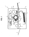
- FIG. 1 is a schematic view illustrating a cross section of an embodiment of the printer of the present invention.
- a body housing 2 having the shape of a chassis of a printer 1 includes a manual feeding tray 3 in which papers to be manually fed are layered and a paper discharge tray 4 from which papers after images are formed on are discharged.
- the body housing 2 includes paper feeding tray 5 in which plural papers are layered and stored.
- the body housing 2 includes paper route 8 running from the paper feeding tray 5 or manual feeding tray 3 to the paper discharge tray 4 through a printer engine 6 and a fixing unit 7.
- papers layered and stored in the manual feeding tray 3 or paper feeding tray 5 are transfer materials.
- the printer engine 6 is constituted of a photoreceptor 9 located in the center thereof, a charging roller 10 uniformly charging a surface of the photoreceptor 9 as a charger, an irradiator irradiating the photoreceptor 9, a developing unit 12 as an image developer, a pre-transfer charger 13, a transfer charger 14 as a transferer, a separation charger 15, a separation pick 16, a pre-cleaning charger 17, a cleaning unit 18, a discharging lamp 19, etc.
- the irradiator 11 includes a light source (not shown) emitting light, a polygon mirror 20 scanning the light emitted from the light source, a motor 21 rotating the polygon mirror 20, a mirror 23 reflecting the light scanned by the polygon mirror toward the photoreceptor 9 through a lens 22, etc.
- a light source not shown
- a polygon mirror 20 scanning the light emitted from the light source
- a motor 21 rotating the polygon mirror 20
- a mirror 23 reflecting the light scanned by the polygon mirror toward the photoreceptor 9 through a lens 22, etc.
- the photoreceptor 9 will be explained. A detailed illustration of the photoreceptor 9 is omitted because of being a known technology.
- the photoreceptor 9 is constituted of a cylindrical or a column-shaped electroconductive substrate 9a and a photosensitive layer 9b formed on a peripheral surface of the electroconductive substrate 9a, and rotates clockwise in Fig. 1 and in the direction indicated by an arrow R' in Fig. 5.
- the photosensitive layer 9b may be a single layer or a multilayer, and a protection layer 9C is formed on the most surface of the photosensitive layer 9b.
- Suitable materials for use as the electroconductive substrate 9a include electroconductive materials, i.e., metals such as Al, Fe, Cu and Au or metal alloys thereof; materials in which a thin layer of a metal such as Al, Ag and Au or a conductive material such as In2O3 and SnO2 is formed on an insulating substrate such as polyester resins, polycarbonate resins, polyimide resins, and glass; and insulators subjected to an electroconductive treatment such as papers subjected to an electroconductive treatment.
- the shape of the electroconductive substrate 9a is not particularly limited, and any electroconductive substrate 9a having the shape of a plate, a drum or a belt can be used.
- the photosensitive layer 9b of the present invention may be a single layer or a multilayer.
- a charge generation layer of the functionally-separated multilayer photosensitive layer 9b including the charge generation layer and a charge transport layer will be explained.
- the charge generation layer is mainly constituted of a charge generation material, and optionally includes a binder resin.
- Suitable charge generation materials include inorganic materials and organic materials. Specific examples of the inorganic charge generation materials include crystalline selenium, amorphous selenium, selenium-tellurium alloys, selenium-tellurium-halogen alloys, selenium-arsenic alloys and amorphous silicon.
- Suitable amorphous silicon includes ones in which a dangling bond is terminated with a hydrogen atom or a halogen atom, or in which a boron atom or a phosphorus atom is doped.
- organic charge generation materials include known materials, for example, phthalocyanine pigments such as metal phthalocyanine and metal-free phthalocyanine, azulenium pigments, squaric acid methine pigments, azo pigments having a carbazole skeleton, azo pigments having a triphenylamine skeleton, azo pigments having a diphenylamine skeleton, azo pigments having a dibenzothiophene skeleton, azo pigments having a fluorenone skeleton, azo pigments having an oxadiazole skeleton, azo pigments having a bisstilbene skeleton, azo pigments having a distyryloxadiazole skeleton, azo pigments having a distyrylcarbazole skeleton, perylene pigments, anthraquinone pigments, polycyclic quinone pigments, quinoneimine pigments, diphenyl methane pigments, triphenyl methine pigment
- binder resin optionally used in the charge generation layer
- binder resins include polyamide resins, polyurethane resins, epoxy resins, polyketone resins, polycarbonate resins, silicone resins, acrylic resins, polyvinyl butyral resins, polyvinyl formal resins, polyvinyl ketone resins, polystyrene resins, poly-N-vinylcarbazole resins, polyacrylamide resins, and the like resins. These resins can be used alone or in combination. Further, a charge transport material may optionally be included in the charge generation layer.
- Suitable methods of forming the charge generation layer include thin film forming methods in a vacuum and casting methods using a solution or a dispersion.
- Such thin film forming methods in a vacuum include vacuum evaporation methods, glow discharge decomposition methods, ion plating methods, sputtering methods, reaction sputtering methods, CVD methods, etc.
- a charge generation layer including the above-mentioned inorganic or organic materials can preferably be formed by these methods.
- the casting methods of forming the charge generation layer include, e.g., preparing a coating liquid by mixing an inorganic or organic charge generation material mentioned above with a solvent such as tetrahydrofuran, cyclohexanone, dioxane, dichloroethane and butanone with a binder resin if necessary, and dispersing the mixture with a ball mill, an attritor, a sand mill, etc. and coating the coating liquid on a substrate, which is diluted if necessary, by a dip coating method, a spray coating method, a bead coating method, etc.
- a solvent such as tetrahydrofuran, cyclohexanone, dioxane, dichloroethane and butanone
- a binder resin if necessary
- the thus prepared charge generation layer preferably has a thickness of from about 0.01 to 5 ⁇ m, and more preferably from 0.05 to 2 ⁇ m.
- the charge transport layer is formed by dissolving a charge transport material and a binder resin with a solvent such as tetrahydrofuran, cyclohexanone, dioxane, dichloroethane and butanone to prepare a coating liquid and coating the liquid on a substrate.
- the coating methods include dip coating methods, spray coating methods, bead coating methods, etc.
- the binder resins for use in the charge transport layer include polycarbonate resins having a good filming property such as bisphenol A type, bisphenol Z type, bisphenol C type polycarbonate resins or their copolymers, polyarylate resins, polysulfone resins, polyester resins, methacrylic resins, polystyrene resins, vinylacetate, epoxy resins and phenoxy resins. These binder resins can be used alone or in combination.
- the charge transport materials for use in the charge transport layer include oxazole derivatives, oxadiazole derivatives (disclosed in Japanese Laid-Open Patent Publications Nos. 52-139065 and 52-139066), imidazole derivatives, triphenylamine derivatives (disclosed in Japanese Patent No. 03035622), benzidine derivatives (disclosed in Japanese Patent Publication No. 58-32372), ⁇ -phenylstilbene derivatives (disclosed in Japanese Laid-Open Patent Publication No. 57-73075), hydrazone derivatives (disclosed in Japanese Laid-Open Patent Publications Nos.
- the thus prepared charge transport layer preferably has a thickness of from 5 to 100 ⁇ m, and more preferably from 10 to 30 ⁇ m.
- the single-layered photosensitive layer 9b When the single-layered photosensitive layer 9b is formed by the casting methods, etc., the charge generation materials, charge transport materials and binder resins mentioned above may be used to form a single-layered photosensitive layer.
- the single-layered photosensitive layer 9b can optionally include a plasticizer and a leveling agent.
- the single-layered photosensitive layer 9b preferably has a thickness of 5 to 100 ⁇ m, and more preferably from 10 to 30 ⁇ m.
- the single-layered photosensitive layer 9b or the charge transport layer of the multilayer photosensitive layer 9b may include a plasticizer and a leveling agent.
- plasticizers typical plasticizers for resins such as dibutylphthalate and dioctylphthalate can be used.
- a content of the plasticizers is preferably from about 0 to 30 parts by weight per 100 parts by weight of the binder resin.
- leveling agent silicone oils such as a dimethyl silicone oil and a methyl phenyl silicone oil, and a polymer or an oligomer having a perfluoroalkyl group in a side chain thereof can be used.
- a content of the leveling agent is preferably from about 0 to 1 part by weight per 100 parts by weight of the binder resin.
- the photosensitive layer of the present invention can include an antioxidant to improve the stability to withstand environmental conditions, namely to avoid decrease of photosensitivity and increase of residual potential.
- the antioxidant may be included in any layer including an organic material, and preferably included in a layer including a charge transport material.
- the antioxidants for use in the photosensitive layer 9b in the present invention include mono-phenol compounds such as 2,6-di-t-butyl-p-cresol, butylated hydroxyanisole, 2,6-di-t-butyl-4-ethylphenol and stearyl- ⁇ -(3,5-di-t-butyl-4-hydroxyphenyl) propionate; bisphenol compounds such as 2,2'-methylene-bis-(4-methyl-6-t-butylphenol), 2,2'-methylene-bis-(4-ethyl-6-t-butylphenol), 4,4'-thiobis-(3-methyl-6-t-butylphenol) and 4,4'-butylidenebis-(3-methyl-6-t-butylphenol); polymer phenol compounds such as 1,1,3-tris-(2-methyl-4-hydroxy-5-t-butylphenyl)butane, 1,3,5-trimethyl-2,4,6-tris(3,5-di-t-but
- antioxidants for rubbers, plastics, and fats and oils, and marketed items thereof can be obtained without difficulty.
- a content of the antioxidant is preferably from 0.1 to 100 parts by weight, and more preferably from 2 to 30 parts by weight per 100 parts by weight of the charge transport material.
- the protection layer 9c for use in the present invention includes at least an inorganic filler and a binder resin.
- the inorganic filler for use in the present invention include titanium oxide, silica, tin oxide, alumina, zirconium oxide, indium oxide, silicon nitride, calcium oxide, zinc oxide, barium sulfate, etc.
- Surface of these fillers may be treated with an organic material or an inorganic material to improve their dispersibility.
- water-repellent treatments treatments using a silane coupling agent, a fluorine-containing silane coupling agent, or a high fatty acid can be used.
- Fillers subjected to treatments using an inorganic material include fillers treated with alumina, zirconia, tin oxide or silica.
- the titanium oxide, silica and alumina realize good abrasion resistance and electrostatic properties of the resultant photoreceptor.
- one of the titanium oxide, silica, alumina and a mixture thereof is included in the protection layer 9c.
- a content of the inorganic filler in the protection layer 9c for use in the present invention is preferably from 3 to 25 % by weight, and more preferably from 5 to 15 % by weight based on total weight of the protection layer 9c.
- the resultant photoreceptor does not have sufficient abrasion resistance.
- a foreign particle such as a carrier adhered on the surface of the resultant photoreceptor occasionally gives a deep damage thereto.
- a charge trap increases and a residual potential after irradiation increases. Therefore, an irradiated part potential increases and a sufficient potential contrast cannot occasionally be obtained.
- the inorganic filler in the protection layer 9c preferably has an average particle diameter of from 0.2 to 0.4 ⁇ m to improve abrasion resistance of the resultant photoreceptor and have the photoreceptor produce high quality images.
- the average particle diameter of the inorganic filler in the protection layer 9c When the average particle diameter of the inorganic filler in the protection layer 9c is too large, a latent image formed on the photoreceptor 9 tends to be disturbed and the resultant image quality deteriorates.
- the average particle diameter of the inorganic filler in the protection layer 9c is too small, a connection of the filler with the binder resin therein becomes weak and the filler is easily released therefrom, resulting in deterioration of abrasion resistance of the resultant photoreceptor.
- the filler becomes a trap for a charge to transport because quite densely arranged when coated, resulting in deterioration of light attenuation properties and increase of residual potential.
- the filler when the average particle diameter of the inorganic filler in the protection layer 9c is too small, the filler easily agglutinate in a protection layer coating liquid and the resultant protection layer 9c does not have a uniform quality.
- Presence probability of the inorganic filler in the protection layer 9c is fixed over the whole protection layer 9c. Therefore, the protection layer 9c does not impair sensitivity and electrostatic properties of the photosensitive layer 9b, nor fineness of the irradiation.
- the fixed presence probability of the inorganic filler in the protection layer 9c can make the protection layer thinner to contribute higher fineness and response of the resultant photoreceptor, and improve abrasion resistance thereof and the resultant image properties.
- An area occupancy rate of the inorganic filler in the protection layer 9c can be controlled by a particle diameter and its distribution of a material used, a formulation of the coating liquid and a coating apparatus.
- the binder resins for use in the protection layer 9c include acrylic resins, polyester resins, polycarbonate resins having a good filming property such as bisphenol A type, bisphenol Z type, bisphenol C type polycarbonate resins or their copolymers, polyarylate resins, polyamide resins, polyurethane resins, polystyrene resins and epoxy resins resins.
- the polycarbonate resins and polyarylate reins are preferably used.
- a charge transport material is preferably included in the protection layer 9c to impart charge transportability thereto and improve electrostatic properties of the resultant photoreceptor.
- the charge transport material the above-mentioned charge transport materials for use in the charge transport layer can be used.
- compositions for the protection layer 9c are dispersed in a solvent such as tetrahydrofuran, cyclohexanone, dioxane, dichloromethane, dichloroethane and butanone to prepare a coating liquid, and the liquid is coated on the photosensitive layer 9b by dip coating methods, spray coating methods and bead coating methods.
- a solvent such as tetrahydrofuran, cyclohexanone, dioxane, dichloromethane, dichloroethane and butanone
- the photoreceptor 9 of the printer 1 of the present invention can optionally include an intermediate layer which is not shown between the electroconductive substrate 9a and the photosensitive layer 9b.
- the intermediate layer for use in the present invention typically includes a resin as a main component.
- Resins forming the intermediate layer preferably have high solubility in a typical organic solvent in consideration of forming the photosensitive layer 9b on the intermediate layer with a solvent.
- Specific examples of the resins include water-soluble resins such as polyvinylalcohol, casein and sodium polyacrylate; alcohol-soluble resins such as nylon copolymers and methoxymethylated nylon; hardened resins forming a three-dimensional network structure such as polyurethane resins, melamine resins, alkyd resins and epoxy resins.
- the intermediate layer can be formed using a proper solvent and coating methods, and preferably has a thickness of from 0.1 to 20 ⁇ m, and more preferably from 0.5 to 10 ⁇ m.
- the developing unit 12 of the present invention is a two-component developing unit which includes a toner case 12a including a developer formed of a toner and a carrier.
- the toner and carrier for use in the developing unit 12 are not particularly limited, and preferably have a small particle diameter for the purpose of high quality images.
- the toner having a small particle diameter means a toner having an average particle diameter of from about 3 to 9 ⁇ m
- the carrier having a small particle diameter means a carrier having an average particle diameter of from about 30 to 60 ⁇ m.
- the developing unit 12 feeds the developer in the toner case 12a to a surface of the photoreceptor 9 with a developing roller 12b to develop an electrostatic latent image formed on the surface of the photoreceptor 9.
- the developed image on the photoreceptor 9 by the developing unit 12 is transferred onto a paper by the transfer charger 14. Then, all the toner forming the developed image are not transferred and some toners remain on the photoreceptor 9. In the present invention, the toner remaining on the photoreceptor 9 after transferred is simply called a residual toner.
- the cleaning unit 18 includes a cleaning brush 25 and an elastic rubber blade 26 as a blade to remove the residual toner on the surface of the photoreceptor 9.
- Fig. 2 is a schematic view illustrating a cross section of the cleaning brush 25, and Fig. 3 is a schematic view illustrating longitudinal section thereof.
- An arrow R in Fig. 2 represents a rotating direction.
- the cleaning brush 25 has a metallic core 27 as an core rotatable in the direction indicated by the arrow R and is supported at a fixed position of the body housing 2.
- Brush fibers 28 are radially formed all over a peripheral surface of the metallic core 27.
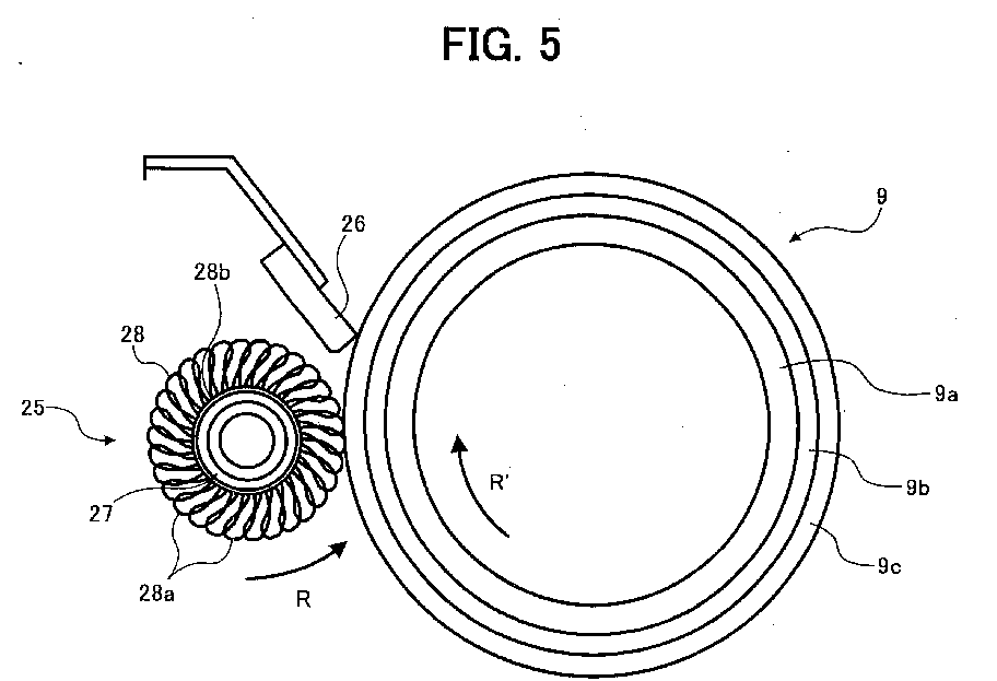
- the cleaning brush 25 rotates in a same direction of the photoreceptor 9 at a contact position of the cleaning brush 25 with the photoreceptor 9 (refer to Fig. 5).
- the brush fiber 28 of the cleaning brush 25 has a loop-shaped top 28a as magnified in Fig. 4.
- the loop-shaped top 28a is positioned on an upstream side from a root 28b of the cleaning brush relative to a rotating direction thereof.
- the cleaning brush 25 is located such that the loop-shaped top 28a contacts the surface of the photoreceptor 9.
- the cleaning brush 25 of the present invention includes a loop pile brush formed of a base cloth 29 on which the brush fibers 28 having loop-shaped tops are formed, which is wound around the metallic core 27.
- Materials forming the brush fiber 28 are not particularly limited, and various known materials such as nylon resins, polyester resins, rayon resins, polycarbonate resins, methacrylic resins and acrylic resins used in typical electrophotographic printers can be used. These resin for use in the materials for the brush fiber 28 can be used alone or in combination.
- the brush fiber 28 may be subjected to an electroconductive treatment.
- the electroconductive treatment includes ordinary methods of coating metals on the surface of a fiber, such as plating methods, vacuum deposition methods and sputtering methods; methods of forming an organic layer including a dispersed polymer in which electroconductive fine particles are dispersed on the surface of a fiber; and methods of blending or polycore compound spinning a polymer in which electroconductive fine particles are dispersed.
- the brush fiber 28 preferably has 50 to 100 loops per 1 cm 2 in terms of its cleanability and durability.
- the elastic rubber blade 26 is, as Fig. 5 shows, located on a downstream side from the cleaning brush 25 relative to the rotating direction R' of the photoreceptor 9 such that a top 26a thereof contacts the photoreceptor 9.
- Any typically used elastic materials such as silicone rubbers and urethane rubbers capable of closely contacting the photoreceptor 9 without abnormally abrading the photoreceptor 9 can be used for the elastic rubber blade 26.
- the thickness of the elastic rubber blade 26 is not particularly limited, and preferably from about 1 to 7 mm.
- a contact pressure of the elastic rubber blade 26 with the photoreceptor 9 is preferably from 10 to 30 g/cm 2 .
- the elastic rubber blade 26 is, as Fig.
- the contact direction of the elastic rubber blade 26 with the photoreceptor 9 is a counter direction against the rotating direction thereof.
- the surface of the photoreceptor 9 uniformly charged with the charging roller 10 is irradiated by the irradiator 11 driven according to image data to form an electrostatic latent image on the photoreceptor 9 in conformity with the image data.
- the developing unit 12 feeds a developer stored in the toner case 12a with the developing roller to the surface of the photoreceptor 9 to develop the electrostatic latent image formed thereon, and the transfer charger 14 transfers the image developed on the photoreceptor 9 onto a transfer sheet.
- the cleaning unit 18 removes a residual toner on the photoreceptor 9 with the cleaning brush 25.
- a line contact of the loop-shaped top 28a of the brush fiber 28 included in the cleaning brush 25 with the surface of the photoreceptor 9 removes foreign particles such as residual toners on the surface thereof without damaging the surface thereof even when the brush fiber is thick and firm.
- the protection layer 9c including an inorganic filler on the most surface of the photoreceptor 9 can improve printability and properly maintain abrasion resistance thereof, and therefore occurrence of abnormal images due to adherence of foreign particles to the photoreceptor 9 can be prevented for a long time and the printer 1 including the photoreceptor 9 can have a long life.
- the brush fiber 28 may have an optional thickness, and preferably has a thickness of from 1 to 50 denier/filament to remove a residual toner after transferred. When less than 1 denier/filament, a residual toner after transferred is not sufficiently removed occasionally according to a sort of the toner. When greater than 50 denier/filament, a surface roughness Rmax (a maximum height of a portion in which a standard length L is removed from a cross-sectional curve) becomes large and defective cleaning occasionally occurs according to a sort of the toner. Therefore, the brush fiber for use in the present invention more preferably has a thickness of from 4 to 20 to maintain its cleanability and surface smoothness of a photoreceptor for a long time.
- top 28a positioned on an upstream side from a root 28b of the brush fiber 28 relative to a rotating direction of the cleaning brush 25 can absorb a contact force of the top 28a of the brush fiber 28 with the surface of the photoreceptor 9 and reduce the running torque of the cleaning brush 25. Therefore, the energy required to drive the cleaning brush 25 can be saved.
- the protection layer 9c formed on the most surface of the photoreceptor 9 includes an inorganic filler having a content of from 3 to 25 % by weight based on total weight of the protection layer 9c, the photoreceptor 9 can improve its printability and properly maintain its abrasion resistance and have a long life.
- the inorganic filler included in the protection layer 9c has an average particle diameter of from 0.2 to 0.4 ⁇ m, an electrostatic latent image can be formed on the photoreceptor 9 without impairing formation of a minute dot while the abrasion resistance thereof is maintained. Therefore, the photoreceptor 9 can produce high quality images and have high durability.
- the inorganic filler included in the protection layer 9c which is selected from the group consisting of titanium oxide, silica, alumina and their mixtures can impart an excellent abrasion resistance to the photoreceptor 9. Therefore, the printer 1 has high durability.
- the toner can be removed by the elastic rubber blade 26 because of being located on a downstream side from the cleaning brush 25 relative to the rotating direction of the photoreceptor 9. Therefore, a foreign particle on the photoreceptor 9 can be removed without fail and occurrence of abnormal images due to adherence of the foreign particle to the photoreceptor 9 can be prevented.
- the elastic rubber blade 26 located on a downstream side from the cleaning brush 25 relative to the rotating direction of the photoreceptor 9 can contact the photoreceptor 9 without fail without a particularly complicated mechanism even while the photoreceptor 9 rotates. Therefore, even when the cleaning brush 25 fails to remove a toner, the toner can be removed by the elastic rubber blade 26 without fail.
- the elastic rubber blade 26 contacts the photoreceptor 9 at a contact pressure of from 10 to 30 g/cm 2 , abnormal abrasion of the photoreceptor 9 can be prevented and a foreign particle thereon can be removed without fail. Therefore, occurrence of abnormal images due to adherence of a foreign particle to the photoreceptor 9 can be prevented for a long time and the printer 1 can have a long life.
- FIG. 6 This embodiment is an application to a copier.
- items having the same numerals as those in Fig. 1 are the same items in Fig. 1 and explanations thereof are omitted.
- Fig. 6 is a schematic view illustrating a cross section of an embodiment of the copier of the present invention.
- a copier 40 is equipped with a scanner 41 scanning an original image and a printer 1 forming the image on a paper, which is scanned by the scanner 41.
- the scanner 41 has a contact glass 42 on which the original (not shown) is set.
- the original is set on the contact glass 42 facing its image side thereon.
- a pressure plate 43 pressing the original onto the contact glass 42 is formed.
- a first traveler 46 having a light source 44 emitting light and a mirror 45
- a second traveler 49 having two mirrors 47 and 48
- a read optical system 53 constituted of a CCD (charge coupled device) image sensor 51 receiving light led by the mirrors 45, 47 and 48 through an imaging lens 50, etc.
- the CCD image sensor 51 works as a photoelectric transferer photoelectrically transferring reflection light from the original imaged on the CCD image sensor 51 to photoelectrically transferred data.
- the photoelectrically transferred data photoelectrically transferred by the CCD image sensor 51 is processed by an image processor (not shown) to become digital image data.
- the first and second travelers 46 and 49 are formed so as to be capable of reciprocating along the contact glass 42, and the first traveler 46 travels at a double speed of that of the second traveler 49 by motors or the like (not shown).
- the printer 1 drives and controls a printer engine 6 based on the digital image data processed by the image processor (not shown) from the photoelectrically transferred data photoelectrically transferred by the CCD image sensor 51 to form an image on a recording medium based on the digital image data.
- the copier 40 can remove foreign particles such as residual toners on the surface of the photoreceptor 9 without damaging the surface thereof, prevent occurrence of abnormal images due to adherence of a foreign particle and stably produce high quality images for a long time.
- the above-mentioned image forming units may be fixedly set in a copier, a facsimile or a printer. However, the image forming units may be set therein as a process cartridge.
- the process cartridge means an image forming unit (or device) including at least a photoreceptor, and one of a charger, an imagewise light irradiator, an image developer, an image transferer, a cleaner and a discharger.
- Fig. 7 illustrates an embodiment of the process cartridge, in which numerals 9 is a photoreceptor, 10 is a charger, 11 is an irradiator, 12b is a developing roller and 25 is a cleaning brush.
- a printer in Example 1 includes a photoreceptor prepared by the following method.
- an intermediate layer coating liquid prepared by mixing and pulverizing with a ball mill the following components was coated by a dip coating method on an electroconductive substrate which is an aluminium drum having a diameter of 100 mm and a length of 360 mm, the coated substrate was heated and dried to have an intermediate layer having a thickness of 3.5 ⁇ m.
- Intermediate coating liquid Alkyd resin Bekkosol 1307-60-EL from Dainippon Ink & Chemicals, Inc.
- 6 Melamine resin Super Bekkamin G-821-60 from Dainippon Ink & Chemicals, Inc.
- Titanium oxide CR-EL from Ishihara Sangyo Kaisha, Ltd.
- Charge generation layer coating liquid prepared by mixing and dispersing with a ball mill the following components was coated on the intermediate layer, the coated substrate was heated and dried to have a charge generation layer having a thickness of 0.2 ⁇ m.
- Charge generation layer coating liquid Y-type oxytitanylphthalocyanine 8 Polyvinylbutyral 5 Methyl ethyl ketone 400
- a charge transport layer coating liquid prepared by mixing and dissolving the following components was coated on the charge generation layer, the coated substrate was heated and dried to have a charge transport layer having a thickness of 23 ⁇ m.
- a protection layer coating liquid prepared by mixing and dispersing with a ball mill the following components was coated on the charge transport layer by a spray coating method to form a protection layer having a thickness of 6.0 ⁇ m.
- Protection layer coating liquid Polycarbonate (Z-polyca from TEIJIN CHEMICALS LTD. having a viscosity-average molecular weight of 50,000) 41.9 Alumina (Sumitomo Chemical Co., Ltd.) 8 Disperser 0.1 Antioxidant 0.64 Charge transport material having the formula (1) 29.3 Cyclohexanone 355.4 Tetrahydrofuran 1,320.5
- the alumina in the protection layer coating liquid has an average particle diameter of 0.30 ⁇ m by controlling a dispersing conditions of the protection layer coating liquid.
- the average particle diameter of the alumina was measured by CAPA-700 from Horiba, Ltd.
- the loop-shaped top of the brush fiber of the cleaning brush is, as Figs. 2 and 4 show, positioned on an upstream side from a root of the cleaning brush relative to a rotating direction R thereof.
- the brush fiber inweaved on the base cloth has a density of 70 pieces/cm 2 and thickness of 10 denier/filament.
- the rotating direction of the cleaning brush in the printer in Example 1 is same as that of the photoreceptor at a contact position of the cleaning brush with the photoreceptor.
- the photoreceptor has a linear speed of 360 mm/sec and the cleaning brush has a linear speed of 400 mm/sec, i.e., 1.11 times as fast as that of the photoreceptor, at a contact position of the cleaning brush with the photoreceptor.
- the contact direction of the elastic rubber blade with the photoreceptor in the printer in Example 1 is a counter direction against the rotating direction of the photoreceptor.
- a contact pressure of the elastic rubber blade with the photoreceptor is 20 g/cm 2 .
- Protection layer coating liquid Polycarbonate (Z-polyca from TEIJIN CHEMICALS LTD. having a viscosity-average molecular weight of 50,000) 50.6 Alumina (Sumitomo Chemical Co., Ltd.) 2.7 Disperser 0.03 Antioxidant 0.31 Charge transport material having the formula (1) 35.4 Cyclohexanone 411.9 Tetrahydrofuran 1,467.2
- Protection layer coating liquid Polycarbonate (Z-polyca from TEIJIN CHEMICALS LTD. having a viscosity-average molecular weight of 50,000) 18.4 Alumina (Sumitomo Chemical Co., Ltd.) 10 Disperser 0.1 Antioxidant 0.64 Charge transport material having the formula (1) 12.9 Cyclohexanone 166.7 Tetrahydrofuran 660.2
- Respective solid image densities; local defects such as black spots, white spots, black stripes and white stripes; and abnormal images such as background fouling were evaluated in a comprehensive manner and classified to three stages, i.e., "good”, “slightly poor” and “poor".
- Irradiated part potential of each photoreceptor when having a charged potential of -800 V was measured.
- Abrasion of each photoreceptor was measured after 500,000 images and 1,000,000 images were produced by an eddy current thickness measurer, Fischer Scope MMS from Fischer Instruments K.K.
- Example 4 The procedures of preparation for the printer in Example 1 were repeated to prepare a printer in Example 4 except for reversing rotating direction of the cleaning brush at a contact position with the photoreceptor and changing the linear speed of the cleaning brush to 360 mm/sec, i.e., a relative linear speed was 720 mm/sec.
- Example 1 The procedures of preparation for the printer in Example 1 were repeated to prepare a printer in Example 5 except for changing the contact pressure of the elastic rubber blade with the photoreceptor to 10 g/cm 2 .
- Example 7 The procedures of preparation for the printer in Example 1 were repeated to prepare a printer in Example 7 except for changing the contact pressure of the elastic rubber blade with the photoreceptor to 30 g/cm 2 .
- Example 8 The procedures of preparation for the printer in Example 1 were repeated to prepare a printer in Example 8 except for changing the contact pressure of the elastic rubber blade with the photoreceptor to 40 g/cm 2 .
- Example 9 The procedures of preparation for the printer in Example 1 were repeated to prepare a printer in Example 9 except for changing the contact direction of the elastic rubber blade with the photoreceptor to the same direction, i.e., a trail direction, as the rotating direction of the photoreceptor instead of the counter direction.
- Example 10 The procedures of preparation for the printer in Example 1 were repeated to prepare a printer in Example 10 except for changing the average particle diameter of the alumina in the protection layer coating liquid to 0.10 ⁇ m by controlling the dispersing conditions.
- Example 11 The procedures of preparation for the printer in Example 1 were repeated to prepare a printer in Example 11 except for changing the average particle diameter of the alumina in the protection layer coating liquid to 0.20 ⁇ m by controlling the dispersing conditions.
- Example 12 The procedures of preparation for the printer in Example 1 were repeated to prepare a printer in Example 12 except for changing the average particle diameter of the alumina in the protection layer coating liquid to 0.40 ⁇ m by controlling the dispersing conditions.
- Example 13 The procedures of preparation for the printer in Example 1 were repeated to prepare a printer in Example 13 except for changing the average particle diameter of the alumina in the protection layer coating liquid to 0.50 ⁇ m by controlling the dispersing conditions.
- Example 14 The procedures of preparation for the printer in Example 1 were repeated to prepare a printer in Example 14 except for changing the average particle diameter of the alumina in the protection layer coating liquid to 0.70 ⁇ m by controlling the dispersing conditions.
- Example 15 The procedures of preparation for the printer in Example 1 were repeated to prepare a printer in Example 15 except for changing the alumina to titanium oxide (CR-97 from Ishihara Sangyo Ishihara Sangyo Kaisha, Ltd.) having an average particle diameter of 0.30 ⁇ m in the protection layer coating liquid.
- alumina titanium oxide (CR-97 from Ishihara Sangyo Ishihara Sangyo Kaisha, Ltd.) having an average particle diameter of 0.30 ⁇ m in the protection layer coating liquid.
- Example 16 The procedures of preparation for the printer in Example 1 were repeated to prepare a printer in Example 16 except for changing the alumina to silica (from Nippon Aerosil Co.) having an average particle diameter of 0.30 ⁇ m in the protection layer coating liquid.
- Example 1 The procedures of preparation for the printer in Example 1 were repeated to prepare a printer in Comparative Example 1 except for excluding the alumina in the protection layer coating liquid.
- Protection layer coating liquid Polycarbonate (Z-polyca from TEIJIN CHEMICALS LTD. having a viscosity-average molecular weight of 50,000) 77.6 Alumina (Sumitomo Chemical Co., Ltd.) 1.33 Disperser 0.02 Antioxidant 0.11 Charge transport material having the formula (1) 54.3 Cyclohexanone 625.2 Tetrahydrofuran 2,200.8
- Protection layer coating liquid Polycarbonate (Z-polyca from TEIJIN CHEMICALS LTD. having a viscosity-average molecular weight of 50,000) 10.5 Alumina (Sumitomo Chemical Co., Ltd.) 8 Disperser 0.1 Antioxidant 0.64 Charge transport material having the formula (1) 7.4 Cyclohexanone 103.8 Tetrahydrofuran 440.2
- Example 1 The procedures of preparation for the printer in Example 1 were repeated to prepare a printer in Comparative Example 4 except for excluding the cleaning brush in the cleaner.
- Example 1 The procedures of preparation for the printer in Example 1 were repeated to prepare a printer in Comparative Example 6 except that the cleaning brush had leiotrichous brush fibers having uniform length instead of the loop-shaped top.
- Example 1 The procedures of preparation for the printer in Example 1 were repeated to prepare a printer in Comparative Example 7 except that the cleaning brush had leiotrichous brush fibers having nonuniform length instead of the loop-shaped top.
Landscapes
- Physics & Mathematics (AREA)
- General Physics & Mathematics (AREA)
- Chemical & Material Sciences (AREA)
- Inorganic Chemistry (AREA)
- Cleaning In Electrography (AREA)
- Photoreceptors In Electrophotography (AREA)
Abstract
An image forming apparatus (1) which includes
Description
- The present invention relates to an image forming apparatus and a copier.
- An electrophotographic process is typically one of image forming methods of charging a photoconductive photoreceptor in a dark place with, e.g., a corona discharge; irradiating the photoreceptor with imagewise light; forming an electrostatic latent image thereon by selectively scattering a charge on the irradiated part thereon; and developing the latent image with a toner including a colorant such as dyes and pigments and a binder such as polymers to form a visual toner image.
- Image forming apparatuses using the electrophotographic process include an electrophotographic printer, etc. Recently, the image forming apparatuses are required to have high durability in addition to producing high-quality images.
- A photoreceptor in the electrophotographic process repeatedly receiving mechanical and chemical influences in repeated charging, irradiating, developing, transferring and cleaning processes gradually deteriorates and wears. A worn photoreceptor causes deterioration of its chargeability and abnormal images. Therefore, longevity of the image forming apparatus using the electrophotographic process depends on longevity of the photoreceptor in many cases, and it is quite essential that a photoreceptor having good abrasion resistance is used for the image forming apparatus to have high durability.
- For example, Japanese Laid-Open Patent Publications Nos. 1-205171, 7-333881, 8-15887, 8-123053 and 8-146641 disclose technologies to improve abrasion resistance of a photoreceptor by forming a protection layer on the most surface thereof and including an inorganic filler in a photosensitive layer thereof.
- However, photoreceptors using the technologies disclosed in Japanese Laid-Open Patent Publications Nos. 1-205171, 7-333881, 8-15887, 8-123053 and 8-146641 have good abrasion resistance, but light portion potentials thereof increase in long-term continuous repeated use and the photoreceptors have drawbacks of image quality deterioration such as image density deterioration. The protection layer on the most surface of a photoreceptor can improve mechanical abrasion resistance thereof. However, when a foreign particle is adhered on a surface of a photoreceptor for some reason, the surface thereof tends to have a scratch causing an image defect. Therefore, it is difficult to make full use of a photoreceptor including a protection layer on the most surface thereof in an electrophotographic process in some regards.
- The foreign particle adhered on a surface of a photoreceptor includes a toner which is not cleaned. A toner adhered on a photoreceptor, which is not cleaned causes defective images. Therefore, even a highly-durable photoreceptor is considered to come to an end of its life, i.e., an image forming apparatus including the photoreceptor is considered to come to an end of its life when producing a defective image.
- Conventionally, a toner having a small particle diameter is used to realize high quality images. Although the toner having a small particle diameter can dramatically improve image quality, it is difficult to clean the toner having a small particle diameter. Therefore, the toner which is not cleaned tends to adhere on a photoreceptor and the problem mentioned above tends to occur.
- In accordance with higher durability of photoreceptors, the problem mentioned above occurs due to not only the toner which is not cleaned but also paper powders, toner additives and other foreign particles because opportunities in which a paper powder caused by a paper used accumulates on photoreceptors, additives in a toner agglutinate thereon and other foreign particles adhere thereon increase.
- In order to cope with the problem, removal of untransferred toner and foreign particles such as paper powders is prioritized, and e.g., it can be considered that a cut-pile shaped cleaning brush having a thicker or firmer base thread than a conventional thread is used to improve toner removal capability and cleanability.
- However, when the cleanability is strengthened more than necessary, a photoreceptor is abnormally abraded or a surface roughness thereof becomes large. Therefore, the photoreceptor cannot sufficiently be cleaned earlier, which causes image defects in many cases. For example, as mentioned above, when the cut-pile shaped cleaning brush having a thicker or firmer base thread is used, a point contact of a cross sectional edge of the thread with a photoreceptor scratches a surface thereof and causes an abnormal abrasion thereof, resulting in image defects.
- Particularly, as mentioned above, when the cleanability is strengthened more than necessary in an image forming apparatus including a photoreceptor including a protection layer on its most surface including an inorganic filler, the filler is easily released from the protection layer and the released filler tends to scratch a surface of the photoreceptor. Such a scratch on the protection layer in which an inorganic filler is dispersed is considered to be caused by an abrasion of the inorganic filler, which is released from the most surface layer as the abrasion thereof proceeds due to long-term repeated use, with the photoreceptor when cleaned. A photoreceptor has innumerable scratches when cleaned unless cleaning conditions are adjusted because the inorganic filler typically has quite a high hardness. A toner which adheres to the scratches and cannot be removed causes defective stripe or micro-spot images.
- Recently, such defective images tend to be produced more when a toner having a small particle diameter, particularly a spheric toner such as a polymerized toner, is used to produce higher quality images. It is difficult to produce high quality images without producing abnormal images and have high durability to keep producing high quality images for a long time.
- Such problems also occur even in an image forming apparatus disclosed in Japanese Laid-Open Patent Publication No. 8-314175, wherein a photoreceptor includes inorganic fine particles in its most surface layer to decrease abrasion of the surface and a rubber blade and a brush are contacted with the photoreceptor to sufficiently clean the photoreceptor.
- As mentioned above, a highly durable photoreceptor which is essential for forming images and, at the same time, a cleaning unit which fully takes advantage of the durability are indispensable for an image forming apparatus producing high quality images and having high durability.
- However, such an image forming apparatus producing high quality images and having high durability is not available.
- Japanese Patents Nos. 2619424 and 2793647 disclose a brush cleaner having a loop-shaped portion which contacts a surface of a photo-receptor to improve cleanability and decrease damages of the photoreceptor due to cleaning. However, higher quality images and higher durability are desired.
- Because of these reasons, a need exists for an image forming apparatus producing high quality images and having high durability.
- Accordingly, an object of the present invention is to prevent production of abnormal images due to adherence of foreign particles to a photoreceptor for a long time, and to extend lives of a photoreceptor and an image forming apparatus including the photoreceptor.
- Briefly these objects and other objects of the present invention as hereinafter will become more readily apparent can be attained by an image forming apparatus which includes a photoreceptor including an electroconductive substrate; a photosensitive layer including a charge generation material and a charge transport material, and overlying the electroconductive substrate; and a protection layer including an inorganic filler in an amount of from 3 to 25 % by weight based on total weight of the protection layer and a binder resin, and overlying the photosensitive layer, a charger charging the photoreceptor; an irradiator forming an electrostatic latent image on the photoreceptor; an image developer developing the electrostatic latent image with a developer including a toner to form a toner image on the photoreceptor; a transferer transferring the toner image onto a transfer material; and a cleaner cleaning the photoreceptor, including a rotatable core and a looped brush fiber provided on the surface of the rotatable core so as to contact the photoreceptor, wherein a top of the looped brush fiber is positioned on an upstream side from a root of the looped brush fiber relative to a rotating direction of the rotatable core.
- These and other objects, features and advantages of the present invention will become apparent upon consideration of the following description of the preferred embodiments of the present invention taken in conjunction with the accompanying drawings.
- Various other objects, features and attendant advantages of the present invention will be more fully appreciated as the same becomes better understood from the detailed description when considered in connection with the accompanying drawings in which like reference characters designate like corresponding parts throughout and wherein:
- Fig. 1 is a schematic view illustrating a cross section of an embodiment of the printer of the present invention;
- Fig. 2 is a schematic view illustrating a cross section of the cleaning brush of the present invention;
- Fig. 3 is a schematic view illustrating longitudinal section of the cleaning brush of the present invention;
- Fig 4 is an enlarged view of a brush fiber of the cleaning brush of the present invention; and
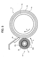
- Fig. 5 is a schematic view illustrating a cross section of a photoreceptor, the cleaning brush and elastic rubber blade of the present invention;
- Fig. 6 is a schematic view illustrating a cross section of an embodiment of the copier of the present invention; and
- Fig. 7 is a schematic view illustrating a cross section of an embodiment of the process cartridge of the present invention.
-
- Generally, the present invention provides an image forming apparatus which includes a photoreceptor including an electroconductive substrate; a photosensitive layer including a charge generation material and a charge transport material, and overlying the electroconductive substrate; and a protection layer including an inorganic filler in an amount of from 3 to 25 % by weight based on total weight of the protection layer and a binder resin, and overlying the photosensitive layer, a charger charging the photoreceptor; an irradiator forming an electrostatic latent image on the photoreceptor; an image developer developing the electrostatic latent image with a developer including a toner to form a toner image on the photoreceptor; a transferer transferring the toner image onto a transfer material; and a cleaner cleaning the photoreceptor, including a rotatable core and a looped brush fiber provided on the surface of the rotatable core so as to contact the photoreceptor, wherein a top of the looped brush fiber is positioned on an upstream side from a root of the looped brush fiber relative to a rotating direction of the rotatable core.
- A line contact of the looped brush fiber with the photoreceptor removes foreign particles such as toners remaining on a surface of the photoreceptor after charged, irradiated and a toner image is transferred onto a transfer material without damaging a surface thereof even when the brush fiber is thick and firm. In addition, a protection layer on the most surface of the photoreceptor, which includes an inorganic filler having a content of from 3 to 25 % by weight based on total weight of the protection layer improves printability and properly maintains abrasion resistance of the photoreceptor. Further, a top of the looped brush fiber positioned on an upstream side from a root thereof relative to a rotating direction of the core absorbs a contact force of the top thereof with the surface of the photoreceptor and decreases a running torque of the cleaning brush.
- When rotating directions of the cleaning brush and photoreceptor are same at a contact position thereof, opportunities in which a foreign particle having a higher hardness than the protection layer and the photoreceptor are frictionized to each other can be decreased even when such a foreign particle is mixed in the brush fibers. Then, foreign particles removal capability of the cleaning brush does not deteriorate because a line contact of the looped brush fiber with the photoreceptor improves foreign particles removal capability of the cleaning brush more than a point contact of the brush fiber. Further, even when the brush fiber is thick and firm, a contact force of the top thereof with the surface of the photoreceptor and a running torque of the cleaning brush can be reduced when rotating directions of the cleaning brush and photoreceptor are same at a contact position thereof.
- An elastic blade contacting the photoreceptor at a point located on a downstream side from the cleaning brush relative to a rotating direction of the photoreceptor can remove a toner which cannot be removed by the cleaning brush.
- The elastic blade having a contact pressure with the photoreceptor of from 10 to 30 g/cm2 can prevent abnormal abrasion of the photoreceptor and remove foreign particles without fail.
- The inorganic filler having an average particle diameter of from 0.2 to 0.4 µm can maintain abrasion resistance of the resultant photoreceptor, which can form an electrostatic latent image without impairing formation of fine dots.
- The inorganic filler selected from the group consisting of titanium oxide, silica, alumina and their mixtures can impart excellent abrasion resistance to the resultant photoreceptor.
- The brush fiber having a thickness of from 4 to 20 denier/filament can maintain its cleanability and surface smoothness of the photoreceptor for a long time.
- An embodiment of the present invention will be explained, referring to Fig. 1 or 5. The embodiment is an example applied for a printer as an image forming apparatus.
- Fig. 1 is a schematic view illustrating a cross section of an embodiment of the printer of the present invention. A
body housing 2 having the shape of a chassis of aprinter 1 includes amanual feeding tray 3 in which papers to be manually fed are layered and apaper discharge tray 4 from which papers after images are formed on are discharged. - The
body housing 2 includespaper feeding tray 5 in which plural papers are layered and stored. Thebody housing 2 includespaper route 8 running from thepaper feeding tray 5 ormanual feeding tray 3 to thepaper discharge tray 4 through aprinter engine 6 and afixing unit 7. In this embodiment, papers layered and stored in themanual feeding tray 3 orpaper feeding tray 5 are transfer materials. - The
printer engine 6 is constituted of aphotoreceptor 9 located in the center thereof, a chargingroller 10 uniformly charging a surface of thephotoreceptor 9 as a charger, an irradiator irradiating thephotoreceptor 9, a developingunit 12 as an image developer, apre-transfer charger 13, atransfer charger 14 as a transferer, a separation charger 15, aseparation pick 16, apre-cleaning charger 17, acleaning unit 18, a discharginglamp 19, etc. - The
irradiator 11 includes a light source (not shown) emitting light, apolygon mirror 20 scanning the light emitted from the light source, amotor 21 rotating thepolygon mirror 20, amirror 23 reflecting the light scanned by the polygon mirror toward thephotoreceptor 9 through alens 22, etc. An explanation of theirradiator 11 is omitted because of being a known technology. - The
photoreceptor 9 will be explained. A detailed illustration of thephotoreceptor 9 is omitted because of being a known technology. Thephotoreceptor 9 is constituted of a cylindrical or a column-shapedelectroconductive substrate 9a and aphotosensitive layer 9b formed on a peripheral surface of theelectroconductive substrate 9a, and rotates clockwise in Fig. 1 and in the direction indicated by an arrow R' in Fig. 5. Thephotosensitive layer 9b may be a single layer or a multilayer, and a protection layer 9C is formed on the most surface of thephotosensitive layer 9b. - Suitable materials for use as the
electroconductive substrate 9a include electroconductive materials, i.e., metals such as Al, Fe, Cu and Au or metal alloys thereof; materials in which a thin layer of a metal such as Al, Ag and Au or a conductive material such as In2O3 and SnO2 is formed on an insulating substrate such as polyester resins, polycarbonate resins, polyimide resins, and glass; and insulators subjected to an electroconductive treatment such as papers subjected to an electroconductive treatment. The shape of theelectroconductive substrate 9a is not particularly limited, and anyelectroconductive substrate 9a having the shape of a plate, a drum or a belt can be used. - Next, the
photosensitive layer 9b will be explained. Thephotosensitive layer 9b of the present invention may be a single layer or a multilayer. First, a charge generation layer of the functionally-separated multilayerphotosensitive layer 9b including the charge generation layer and a charge transport layer will be explained. - The charge generation layer is mainly constituted of a charge generation material, and optionally includes a binder resin. Suitable charge generation materials include inorganic materials and organic materials. Specific examples of the inorganic charge generation materials include crystalline selenium, amorphous selenium, selenium-tellurium alloys, selenium-tellurium-halogen alloys, selenium-arsenic alloys and amorphous silicon. Suitable amorphous silicon includes ones in which a dangling bond is terminated with a hydrogen atom or a halogen atom, or in which a boron atom or a phosphorus atom is doped. Specific examples of the organic charge generation materials include known materials, for example, phthalocyanine pigments such as metal phthalocyanine and metal-free phthalocyanine, azulenium pigments, squaric acid methine pigments, azo pigments having a carbazole skeleton, azo pigments having a triphenylamine skeleton, azo pigments having a diphenylamine skeleton, azo pigments having a dibenzothiophene skeleton, azo pigments having a fluorenone skeleton, azo pigments having an oxadiazole skeleton, azo pigments having a bisstilbene skeleton, azo pigments having a distyryloxadiazole skeleton, azo pigments having a distyrylcarbazole skeleton, perylene pigments, anthraquinone pigments, polycyclic quinone pigments, quinoneimine pigments, diphenyl methane pigments, triphenyl methane pigments, benzoquinone pigments, naphthoquinone pigments, cyanine pigments, azomethine pigments, indigoid pigments, bisbenzimidazole pigments and the like materials. These charge transport materials can be used alone or in combination.
- Specific examples of the binder resin optionally used in the charge generation layer include polyamide resins, polyurethane resins, epoxy resins, polyketone resins, polycarbonate resins, silicone resins, acrylic resins, polyvinyl butyral resins, polyvinyl formal resins, polyvinyl ketone resins, polystyrene resins, poly-N-vinylcarbazole resins, polyacrylamide resins, and the like resins. These resins can be used alone or in combination. Further, a charge transport material may optionally be included in the charge generation layer.
- Suitable methods of forming the charge generation layer include thin film forming methods in a vacuum and casting methods using a solution or a dispersion.
- Specific examples of such thin film forming methods in a vacuum include vacuum evaporation methods, glow discharge decomposition methods, ion plating methods, sputtering methods, reaction sputtering methods, CVD methods, etc. A charge generation layer including the above-mentioned inorganic or organic materials can preferably be formed by these methods.
- The casting methods of forming the charge generation layer include, e.g., preparing a coating liquid by mixing an inorganic or organic charge generation material mentioned above with a solvent such as tetrahydrofuran, cyclohexanone, dioxane, dichloroethane and butanone with a binder resin if necessary, and dispersing the mixture with a ball mill, an attritor, a sand mill, etc. and coating the coating liquid on a substrate, which is diluted if necessary, by a dip coating method, a spray coating method, a bead coating method, etc.
- The thus prepared charge generation layer preferably has a thickness of from about 0.01 to 5 µm, and more preferably from 0.05 to 2 µm.
- Next, a charge transport layer will be explained. The charge transport layer is formed by dissolving a charge transport material and a binder resin with a solvent such as tetrahydrofuran, cyclohexanone, dioxane, dichloroethane and butanone to prepare a coating liquid and coating the liquid on a substrate. The coating methods include dip coating methods, spray coating methods, bead coating methods, etc.
- The binder resins for use in the charge transport layer include polycarbonate resins having a good filming property such as bisphenol A type, bisphenol Z type, bisphenol C type polycarbonate resins or their copolymers, polyarylate resins, polysulfone resins, polyester resins, methacrylic resins, polystyrene resins, vinylacetate, epoxy resins and phenoxy resins. These binder resins can be used alone or in combination.
- The charge transport materials for use in the charge transport layer include oxazole derivatives, oxadiazole derivatives (disclosed in Japanese Laid-Open Patent Publications Nos. 52-139065 and 52-139066), imidazole derivatives, triphenylamine derivatives (disclosed in Japanese Patent No. 03035622), benzidine derivatives (disclosed in Japanese Patent Publication No. 58-32372), α-phenylstilbene derivatives (disclosed in Japanese Laid-Open Patent Publication No. 57-73075), hydrazone derivatives (disclosed in Japanese Laid-Open Patent Publications Nos. 55-154955, 55-156954, 55-52063 and 56-81850), triphenylmethane derivatives (disclosed in Japanese Laid-Open Patent Publication No. 51-94829), styryl derivatives (disclosed in Japanese Laid-Open Patent Publications Nos. 56-29245 and 58-58552), pyrene derivatives (disclosed in Japanese Patent No. 03081662), etc.
- The thus prepared charge transport layer preferably has a thickness of from 5 to 100 µm, and more preferably from 10 to 30 µm.
- Next, the single-layered
photosensitive layer 9b will be explained. When the single-layeredphotosensitive layer 9b is formed by the casting methods, etc., the charge generation materials, charge transport materials and binder resins mentioned above may be used to form a single-layered photosensitive layer. The single-layeredphotosensitive layer 9b can optionally include a plasticizer and a leveling agent. The single-layeredphotosensitive layer 9b preferably has a thickness of 5 to 100 µm, and more preferably from 10 to 30 µm. - In the present invention, the single-layered
photosensitive layer 9b or the charge transport layer of the multilayerphotosensitive layer 9b may include a plasticizer and a leveling agent. As the plasticizers, typical plasticizers for resins such as dibutylphthalate and dioctylphthalate can be used. A content of the plasticizers is preferably from about 0 to 30 parts by weight per 100 parts by weight of the binder resin. As the leveling agent, silicone oils such as a dimethyl silicone oil and a methyl phenyl silicone oil, and a polymer or an oligomer having a perfluoroalkyl group in a side chain thereof can be used. A content of the leveling agent is preferably from about 0 to 1 part by weight per 100 parts by weight of the binder resin. - The photosensitive layer of the present invention can include an antioxidant to improve the stability to withstand environmental conditions, namely to avoid decrease of photosensitivity and increase of residual potential. The antioxidant may be included in any layer including an organic material, and preferably included in a layer including a charge transport material.
- The antioxidants for use in the photosensitive layer 9b in the present invention include mono-phenol compounds such as 2,6-di-t-butyl-p-cresol, butylated hydroxyanisole, 2,6-di-t-butyl-4-ethylphenol and stearyl-β-(3,5-di-t-butyl-4-hydroxyphenyl) propionate; bisphenol compounds such as 2,2'-methylene-bis-(4-methyl-6-t-butylphenol), 2,2'-methylene-bis-(4-ethyl-6-t-butylphenol), 4,4'-thiobis-(3-methyl-6-t-butylphenol) and 4,4'-butylidenebis-(3-methyl-6-t-butylphenol); polymer phenol compounds such as 1,1,3-tris-(2-methyl-4-hydroxy-5-t-butylphenyl)butane, 1,3,5-trimethyl-2,4,6-tris(3,5-di-t-butyl-4-hydroxybenzyl)benzene, tetrakis-[methylene-3-(3',5'-di-t-butyl-4'-hydroxyphenyl)propionate]methane, bis[3,3'-bis(4'-hydroxy-3'-t-butylphenyl)butyric acid]glycol ester and tocophenol compounds; paraphenylenediamine compounds such as N-phenyl-N'-isopropyl-p-phenylenediamine, N,N'-di-sec-butyl-p-phenylenediamine, N-phenyl-N-sec-butyl-p-phenylenediamine, N,N'-di-isopropyl-p-phenylenediamine and N,N'-dimethyl-N,N'-di-t-butyl-p-phenylenediamine; hydroquinone compounds such as 2,5-di-t-octylhydroquinone, 2,6-didodecylhydroquinone, 2-dodecylhydroquinone, 2-dodecyl-5-chlorohydroquinone, 2-t-octyl-5-methylhydroquinone and 2-(2-octadecenyl)-5-methylhydroquinone; organic sulfur-containing compounds such as dilauryl-3,3'-thiodipropionate, distearyl-3,3'-thiodipropionate and ditetradecyl-3,3'-thiodipropionate; and organic phosphorus-containing compounds such as triphenylphosphine, tri(nonylphenyl)phosphine, tri(dinonylphenyl)phosphine, tricresylphosphine and tri(2,4-dibutylphenoxy)phosphine.
- These compounds are known as antioxidants for rubbers, plastics, and fats and oils, and marketed items thereof can be obtained without difficulty.
- In the present invention, a content of the antioxidant is preferably from 0.1 to 100 parts by weight, and more preferably from 2 to 30 parts by weight per 100 parts by weight of the charge transport material.
- Next, the
protection layer 9c for use in the present invention will be explained. Theprotection layer 9c for use in the present invention includes at least an inorganic filler and a binder resin. - Specific examples of the inorganic filler for use in the present invention include titanium oxide, silica, tin oxide, alumina, zirconium oxide, indium oxide, silicon nitride, calcium oxide, zinc oxide, barium sulfate, etc. Surface of these fillers may be treated with an organic material or an inorganic material to improve their dispersibility. As water-repellent treatments, treatments using a silane coupling agent, a fluorine-containing silane coupling agent, or a high fatty acid can be used. Fillers subjected to treatments using an inorganic material include fillers treated with alumina, zirconia, tin oxide or silica. Above all, the titanium oxide, silica and alumina realize good abrasion resistance and electrostatic properties of the resultant photoreceptor. In the present invention, one of the titanium oxide, silica, alumina and a mixture thereof is included in the
protection layer 9c. - A content of the inorganic filler in the
protection layer 9c for use in the present invention is preferably from 3 to 25 % by weight, and more preferably from 5 to 15 % by weight based on total weight of theprotection layer 9c. - When the content of the inorganic filler is less than 3 % by weight based on total weight of the
protection layer 9c, the resultant photoreceptor does not have sufficient abrasion resistance. When greater than 25 % by weight, a foreign particle such as a carrier adhered on the surface of the resultant photoreceptor occasionally gives a deep damage thereto. In addition, when greater than 25 %, a charge trap increases and a residual potential after irradiation increases. Therefore, an irradiated part potential increases and a sufficient potential contrast cannot occasionally be obtained. - The inorganic filler in the
protection layer 9c preferably has an average particle diameter of from 0.2 to 0.4 µm to improve abrasion resistance of the resultant photoreceptor and have the photoreceptor produce high quality images. - When the average particle diameter of the inorganic filler in the
protection layer 9c is too large, a latent image formed on thephotoreceptor 9 tends to be disturbed and the resultant image quality deteriorates. When the average particle diameter of the inorganic filler in theprotection layer 9c is too small, a connection of the filler with the binder resin therein becomes weak and the filler is easily released therefrom, resulting in deterioration of abrasion resistance of the resultant photoreceptor. In addition, when the average particle diameter of the inorganic filler in theprotection layer 9c is extremely small, the filler becomes a trap for a charge to transport because quite densely arranged when coated, resulting in deterioration of light attenuation properties and increase of residual potential. Further, when the average particle diameter of the inorganic filler in theprotection layer 9c is too small, the filler easily agglutinate in a protection layer coating liquid and theresultant protection layer 9c does not have a uniform quality. These problems can be solved by the filler having an average particle diameter of from 0.2 to 0.4 µm. - Presence probability of the inorganic filler in the
protection layer 9c is fixed over thewhole protection layer 9c. Therefore, theprotection layer 9c does not impair sensitivity and electrostatic properties of thephotosensitive layer 9b, nor fineness of the irradiation. The fixed presence probability of the inorganic filler in theprotection layer 9c can make the protection layer thinner to contribute higher fineness and response of the resultant photoreceptor, and improve abrasion resistance thereof and the resultant image properties. An area occupancy rate of the inorganic filler in theprotection layer 9c can be controlled by a particle diameter and its distribution of a material used, a formulation of the coating liquid and a coating apparatus. - The binder resins for use in the
protection layer 9c include acrylic resins, polyester resins, polycarbonate resins having a good filming property such as bisphenol A type, bisphenol Z type, bisphenol C type polycarbonate resins or their copolymers, polyarylate resins, polyamide resins, polyurethane resins, polystyrene resins and epoxy resins resins. In particular, the polycarbonate resins and polyarylate reins are preferably used. - A charge transport material is preferably included in the
protection layer 9c to impart charge transportability thereto and improve electrostatic properties of the resultant photoreceptor. As the charge transport material, the above-mentioned charge transport materials for use in the charge transport layer can be used. - These compositions for the
protection layer 9c are dispersed in a solvent such as tetrahydrofuran, cyclohexanone, dioxane, dichloromethane, dichloroethane and butanone to prepare a coating liquid, and the liquid is coated on thephotosensitive layer 9b by dip coating methods, spray coating methods and bead coating methods. - The
photoreceptor 9 of theprinter 1 of the present invention can optionally include an intermediate layer which is not shown between theelectroconductive substrate 9a and thephotosensitive layer 9b. The intermediate layer for use in the present invention typically includes a resin as a main component. Resins forming the intermediate layer preferably have high solubility in a typical organic solvent in consideration of forming thephotosensitive layer 9b on the intermediate layer with a solvent. Specific examples of the resins include water-soluble resins such as polyvinylalcohol, casein and sodium polyacrylate; alcohol-soluble resins such as nylon copolymers and methoxymethylated nylon; hardened resins forming a three-dimensional network structure such as polyurethane resins, melamine resins, alkyd resins and epoxy resins. In addition, fine powders of metal oxides such as titanium oxide, silica, alumina, zirconium oxide, tin oxide and indium oxide, metal sulfides or metal nitrides, etc. included in the intermediate layer as a filler can further maintain stable chargeability of the resultant photoreceptor. The intermediate layer can be formed using a proper solvent and coating methods, and preferably has a thickness of from 0.1 to 20 µm, and more preferably from 0.5 to 10 µm. - Next, the developing
unit 12 will be explained. The developingunit 12 of the present invention is a two-component developing unit which includes atoner case 12a including a developer formed of a toner and a carrier. The toner and carrier for use in the developingunit 12 are not particularly limited, and preferably have a small particle diameter for the purpose of high quality images. Typically, the toner having a small particle diameter means a toner having an average particle diameter of from about 3 to 9 µm, and the carrier having a small particle diameter means a carrier having an average particle diameter of from about 30 to 60 µm. In forming an image, the developingunit 12 feeds the developer in thetoner case 12a to a surface of thephotoreceptor 9 with a developingroller 12b to develop an electrostatic latent image formed on the surface of thephotoreceptor 9. - The developed image on the
photoreceptor 9 by the developingunit 12 is transferred onto a paper by thetransfer charger 14. Then, all the toner forming the developed image are not transferred and some toners remain on thephotoreceptor 9. In the present invention, the toner remaining on thephotoreceptor 9 after transferred is simply called a residual toner. - The
cleaning unit 18 includes a cleaningbrush 25 and anelastic rubber blade 26 as a blade to remove the residual toner on the surface of thephotoreceptor 9. - Fig. 2 is a schematic view illustrating a cross section of the cleaning
brush 25, and Fig. 3 is a schematic view illustrating longitudinal section thereof. An arrow R in Fig. 2 represents a rotating direction. The cleaningbrush 25 has ametallic core 27 as an core rotatable in the direction indicated by the arrow R and is supported at a fixed position of thebody housing 2.Brush fibers 28 are radially formed all over a peripheral surface of themetallic core 27. The cleaningbrush 25 rotates in a same direction of thephotoreceptor 9 at a contact position of the cleaningbrush 25 with the photoreceptor 9 (refer to Fig. 5). Thebrush fiber 28 of the cleaningbrush 25 has a loop-shaped top 28a as magnified in Fig. 4. The loop-shaped top 28a is positioned on an upstream side from aroot 28b of the cleaning brush relative to a rotating direction thereof. The cleaningbrush 25 is located such that the loop-shaped top 28a contacts the surface of thephotoreceptor 9. The cleaningbrush 25 of the present invention includes a loop pile brush formed of abase cloth 29 on which thebrush fibers 28 having loop-shaped tops are formed, which is wound around themetallic core 27. - Materials forming the
brush fiber 28 are not particularly limited, and various known materials such as nylon resins, polyester resins, rayon resins, polycarbonate resins, methacrylic resins and acrylic resins used in typical electrophotographic printers can be used. These resin for use in the materials for thebrush fiber 28 can be used alone or in combination. - In addition, the
brush fiber 28 may be subjected to an electroconductive treatment. The electroconductive treatment includes ordinary methods of coating metals on the surface of a fiber, such as plating methods, vacuum deposition methods and sputtering methods; methods of forming an organic layer including a dispersed polymer in which electroconductive fine particles are dispersed on the surface of a fiber; and methods of blending or polycore compound spinning a polymer in which electroconductive fine particles are dispersed. Thebrush fiber 28 preferably has 50 to 100 loops per 1 cm2 in terms of its cleanability and durability. - The
elastic rubber blade 26 is, as Fig. 5 shows, located on a downstream side from the cleaningbrush 25 relative to the rotating direction R' of thephotoreceptor 9 such that a top 26a thereof contacts thephotoreceptor 9. Any typically used elastic materials such as silicone rubbers and urethane rubbers capable of closely contacting thephotoreceptor 9 without abnormally abrading thephotoreceptor 9 can be used for theelastic rubber blade 26. The thickness of theelastic rubber blade 26 is not particularly limited, and preferably from about 1 to 7 mm. A contact pressure of theelastic rubber blade 26 with thephotoreceptor 9 is preferably from 10 to 30 g/cm2. In addition, theelastic rubber blade 26 is, as Fig. 5 shows, located on a downstream side from the cleaningbrush 25 relative to the rotating direction of thephotoreceptor 9 and contacted with thephotoreceptor 9. Therefore, the contact direction of theelastic rubber blade 26 with thephotoreceptor 9 is a counter direction against the rotating direction thereof. - The surface of the
photoreceptor 9 uniformly charged with the chargingroller 10 is irradiated by theirradiator 11 driven according to image data to form an electrostatic latent image on thephotoreceptor 9 in conformity with the image data. The developingunit 12 feeds a developer stored in thetoner case 12a with the developing roller to the surface of thephotoreceptor 9 to develop the electrostatic latent image formed thereon, and thetransfer charger 14 transfers the image developed on thephotoreceptor 9 onto a transfer sheet. - First, the
cleaning unit 18 removes a residual toner on thephotoreceptor 9 with the cleaningbrush 25. A line contact of the loop-shaped top 28a of thebrush fiber 28 included in the cleaningbrush 25 with the surface of thephotoreceptor 9 removes foreign particles such as residual toners on the surface thereof without damaging the surface thereof even when the brush fiber is thick and firm. In addition, theprotection layer 9c including an inorganic filler on the most surface of thephotoreceptor 9 can improve printability and properly maintain abrasion resistance thereof, and therefore occurrence of abnormal images due to adherence of foreign particles to thephotoreceptor 9 can be prevented for a long time and theprinter 1 including thephotoreceptor 9 can have a long life. - The
brush fiber 28 may have an optional thickness, and preferably has a thickness of from 1 to 50 denier/filament to remove a residual toner after transferred. When less than 1 denier/filament, a residual toner after transferred is not sufficiently removed occasionally according to a sort of the toner. When greater than 50 denier/filament, a surface roughness Rmax (a maximum height of a portion in which a standard length L is removed from a cross-sectional curve) becomes large and defective cleaning occasionally occurs according to a sort of the toner. Therefore, the brush fiber for use in the present invention more preferably has a thickness of from 4 to 20 to maintain its cleanability and surface smoothness of a photoreceptor for a long time. - Because the rotating directions of the cleaning
brush 25 and thephotoreceptor 9 are same at a contact position thereof, even when a foreign particle having a higher hardness than theprotection layer 9c is mixed in thebrush fibers 28, chances that the foreign particle and thephotoreceptor 9 are in friction can be decreased and possibility that thephotoreceptor 9 is damaged can be decreased. - Because of a line contact of the loop-shaped top 28a of the
brush fiber 28 with the surface of thephotoreceptor 9, foreign particle removal capability of the cleaningbrush 25 can be improved, compared with a contact point of the conventional cleaning brush contacting its cut surface with the photoreceptor. Therefore, even when the rotating directions of the cleaningbrush 25 and thephotoreceptor 9 are same at a contact position thereof, the foreign particle removal capability of the cleaningbrush 25 does not deteriorate. - Because the rotating directions of the cleaning
brush 25 and thephotoreceptor 9 are same at a contact position thereof, even when thebrush fiber 28 is thick and firm, a contact force of the top 28a of thebrush fiber 28 with the surface of thephotoreceptor 9 can be absorbed and a running torque of the cleaningbrush 25 can be reduced. Therefore, an energy required to drive the cleaningbrush 25 can be saved. - Further, the top 28a positioned on an upstream side from a
root 28b of thebrush fiber 28 relative to a rotating direction of the cleaningbrush 25 can absorb a contact force of the top 28a of thebrush fiber 28 with the surface of thephotoreceptor 9 and reduce the running torque of the cleaningbrush 25. Therefore, the energy required to drive the cleaningbrush 25 can be saved. - In addition, because the
protection layer 9c formed on the most surface of thephotoreceptor 9 includes an inorganic filler having a content of from 3 to 25 % by weight based on total weight of theprotection layer 9c, thephotoreceptor 9 can improve its printability and properly maintain its abrasion resistance and have a long life. - Because the inorganic filler included in the
protection layer 9c has an average particle diameter of from 0.2 to 0.4 µm, an electrostatic latent image can be formed on thephotoreceptor 9 without impairing formation of a minute dot while the abrasion resistance thereof is maintained. Therefore, thephotoreceptor 9 can produce high quality images and have high durability. - Further, the inorganic filler included in the
protection layer 9c, which is selected from the group consisting of titanium oxide, silica, alumina and their mixtures can impart an excellent abrasion resistance to thephotoreceptor 9. Therefore, theprinter 1 has high durability. - In addition, in the
printer 1 of the present invention, even when the cleaningbrush 25 fails to remove a toner, the toner can be removed by theelastic rubber blade 26 because of being located on a downstream side from the cleaningbrush 25 relative to the rotating direction of thephotoreceptor 9. Therefore, a foreign particle on thephotoreceptor 9 can be removed without fail and occurrence of abnormal images due to adherence of the foreign particle to thephotoreceptor 9 can be prevented. - The
elastic rubber blade 26 located on a downstream side from the cleaningbrush 25 relative to the rotating direction of thephotoreceptor 9 can contact thephotoreceptor 9 without fail without a particularly complicated mechanism even while thephotoreceptor 9 rotates. Therefore, even when the cleaningbrush 25 fails to remove a toner, the toner can be removed by theelastic rubber blade 26 without fail. - In addition, because the
elastic rubber blade 26 contacts thephotoreceptor 9 at a contact pressure of from 10 to 30 g/cm2, abnormal abrasion of thephotoreceptor 9 can be prevented and a foreign particle thereon can be removed without fail. Therefore, occurrence of abnormal images due to adherence of a foreign particle to thephotoreceptor 9 can be prevented for a long time and theprinter 1 can have a long life. - Next, another embodiment of the present invention will be explained, referring to Fig. 6. This embodiment is an application to a copier. In Fig. 6, items having the same numerals as those in Fig. 1 are the same items in Fig. 1 and explanations thereof are omitted.
- Fig. 6 is a schematic view illustrating a cross section of an embodiment of the copier of the present invention. In Fig. 6, a
copier 40 is equipped with ascanner 41 scanning an original image and aprinter 1 forming the image on a paper, which is scanned by thescanner 41. - The
scanner 41 has acontact glass 42 on which the original (not shown) is set. The original is set on thecontact glass 42 facing its image side thereon. Above thecontact glass 42, apressure plate 43 pressing the original onto thecontact glass 42 is formed. Below thecontact glass 42, afirst traveler 46 having alight source 44 emitting light and amirror 45, asecond traveler 49 having twomirrors image sensor 51 receiving light led by themirrors imaging lens 50, etc. are formed. TheCCD image sensor 51 works as a photoelectric transferer photoelectrically transferring reflection light from the original imaged on theCCD image sensor 51 to photoelectrically transferred data. The photoelectrically transferred data photoelectrically transferred by theCCD image sensor 51 is processed by an image processor (not shown) to become digital image data. The first andsecond travelers contact glass 42, and thefirst traveler 46 travels at a double speed of that of thesecond traveler 49 by motors or the like (not shown). - The
printer 1 drives and controls aprinter engine 6 based on the digital image data processed by the image processor (not shown) from the photoelectrically transferred data photoelectrically transferred by theCCD image sensor 51 to form an image on a recording medium based on the digital image data. - The
copier 40 can remove foreign particles such as residual toners on the surface of thephotoreceptor 9 without damaging the surface thereof, prevent occurrence of abnormal images due to adherence of a foreign particle and stably produce high quality images for a long time. - The above-mentioned image forming units may be fixedly set in a copier, a facsimile or a printer. However, the image forming units may be set therein as a process cartridge. The process cartridge means an image forming unit (or device) including at least a photoreceptor, and one of a charger, an imagewise light irradiator, an image developer, an image transferer, a cleaner and a discharger. Various process cartridges can be used in the present invention. Fig. 7 illustrates an embodiment of the process cartridge, in which
numerals 9 is a photoreceptor, 10 is a charger, 11 is an irradiator, 12b is a developing roller and 25 is a cleaning brush. - Having generally described this invention, further understanding can be obtained by reference to certain specific examples which are provided herein for the purpose of illustration only and are not intended to be limiting. In the descriptions in the following examples, the numbers represent weight ratios in parts, unless otherwise specified.
- A printer in Example 1 includes a photoreceptor prepared by the following method.
- After an intermediate layer coating liquid prepared by mixing and pulverizing with a ball mill the following components was coated by a dip coating method on an electroconductive substrate which is an aluminium drum having a diameter of 100 mm and a length of 360 mm, the coated substrate was heated and dried to have an intermediate layer having a thickness of 3.5 µm.
Intermediate coating liquid Alkyd resin
(Bekkosol 1307-60-EL from Dainippon Ink & Chemicals, Inc.)6 Melamine resin
(Super Bekkamin G-821-60 from Dainippon Ink & Chemicals, Inc.)4 Titanium oxide
(CR-EL from Ishihara Sangyo Kaisha, Ltd.)40 Methyl ethyl ketone 200 - After a charge generation layer coating liquid prepared by mixing and dispersing with a ball mill the following components was coated on the intermediate layer, the coated substrate was heated and dried to have a charge generation layer having a thickness of 0.2 µm.
Charge generation layer coating liquid Y- type oxytitanylphthalocyanine 8 Polyvinylbutyral 5 Methyl ethyl ketone 400 - After a charge transport layer coating liquid prepared by mixing and dissolving the following components was coated on the charge generation layer, the coated substrate was heated and dried to have a charge transport layer having a thickness of 23 µm.
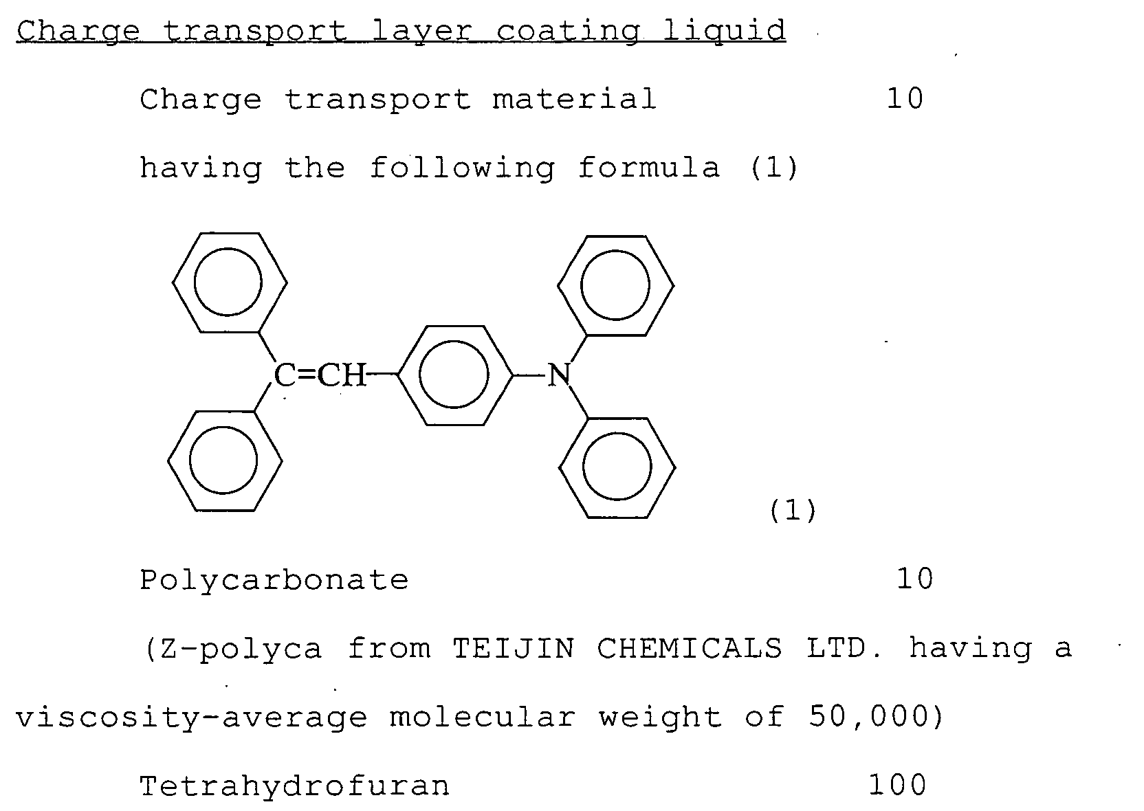
- A protection layer coating liquid prepared by mixing and dispersing with a ball mill the following components was coated on the charge transport layer by a spray coating method to form a protection layer having a thickness of 6.0 µm.
Protection layer coating liquid Polycarbonate
(Z-polyca from TEIJIN CHEMICALS LTD.
having a viscosity-average molecular weight of 50,000)41.9 Alumina
(Sumitomo Chemical Co., Ltd.)8 Disperser 0.1 Antioxidant 0.64 Charge transport material
having the formula (1)29.3 Cyclohexanone 355.4 Tetrahydrofuran 1,320.5 - The alumina in the protection layer coating liquid has an average particle diameter of 0.30 µm by controlling a dispersing conditions of the protection layer coating liquid. The average particle diameter of the alumina was measured by CAPA-700 from Horiba, Ltd.
- The printer in Example 1, as Fig. 2 shows, includes a cleaning brush formed by winding and adhering a loop pile brush formed of the base cloth and brush fibers having a loop-shaped top inweaved thereon around the metallic core. The loop-shaped top of the brush fiber of the cleaning brush is, as Figs. 2 and 4 show, positioned on an upstream side from a root of the cleaning brush relative to a rotating direction R thereof. The brush fiber inweaved on the base cloth has a density of 70 pieces/cm2 and thickness of 10 denier/filament.
- In addition, the rotating direction of the cleaning brush in the printer in Example 1 is same as that of the photoreceptor at a contact position of the cleaning brush with the photoreceptor. The photoreceptor has a linear speed of 360 mm/sec and the cleaning brush has a linear speed of 400 mm/sec, i.e., 1.11 times as fast as that of the photoreceptor, at a contact position of the cleaning brush with the photoreceptor.
- Further, the contact direction of the elastic rubber blade with the photoreceptor in the printer in Example 1 is a counter direction against the rotating direction of the photoreceptor. A contact pressure of the elastic rubber blade with the photoreceptor is 20 g/cm2.
- The procedures of preparation for the printer in Example 1 were repeated to prepare a printer in Example 2 except for changing the formulation of the protection layer coating liquid as follows.
Protection layer coating liquid Polycarbonate
(Z-polyca from TEIJIN CHEMICALS LTD. having a
viscosity-average molecular weight of 50,000)50.6 Alumina
(Sumitomo Chemical Co., Ltd.)2.7 Disperser 0.03 Antioxidant 0.31 Charge transport material
having the formula (1)35.4 Cyclohexanone 411.9 Tetrahydrofuran 1,467.2 - The procedures of preparation for the printer in Example 1 were repeated to prepare a printer in Example 3 except for changing the formulation of the protection layer coating liquid as follows.
Protection layer coating liquid Polycarbonate
(Z-polyca from TEIJIN CHEMICALS LTD. having a
viscosity-average molecular weight of 50,000)18.4 Alumina
(Sumitomo Chemical Co., Ltd.)10 Disperser 0.1 Antioxidant 0.64 Charge transport material
having the formula (1)12.9 Cyclohexanone 166.7 Tetrahydrofuran 660.2 - Subsequently, after 500,000 images and 1,000,000 images were produced by the printers prepared in Examples 1 to 3, the following items were evaluated.
- Respective solid image densities; local defects such as black spots, white spots, black stripes and white stripes; and abnormal images such as background fouling were evaluated in a comprehensive manner and classified to three stages, i.e., "good", "slightly poor" and "poor".
- Irradiated part potential of each photoreceptor when having a charged potential of -800 V was measured.
- Abrasion of each photoreceptor was measured after 500,000 images and 1,000,000 images were produced by an eddy current thickness measurer, Fischer Scope MMS from Fischer Instruments K.K.
- Surface damages of each photoreceptor were observed by a laser microscope VK-8500 from Keyence Corp. and classified to three stages, i.e., ○ represents no particular damage, Δ represents a damage which can be identified by the microscope, but has no influence on the resultant images and × represents a large and deep damage influencing the resultant images.
- The evaluation results are shown in the following Table 1.
After 500,000 After 1,000,000 Image
qualityIrradiated
part
potential (-V)Abrasion of
photoreceptor
(µm)Surface
damage
of
photoreceptorImage
qualityIrradiated
part
potential
(-V)Abrasion of
photoreceptor
(µm)Surface
damage
of
photoreceptorEx. 1 Good 120 2.2 ○ Good 150 4.1 ○ Ex. 2 Good 100 3.1 ○ Good 120 4.7 ○ Ex. 3 Good 140 1.5 ○ Good 160 2.6 Δ - The procedures of preparation for the printer in Example 1 were repeated to prepare a printer in Example 4 except for reversing rotating direction of the cleaning brush at a contact position with the photoreceptor and changing the linear speed of the cleaning brush to 360 mm/sec, i.e., a relative linear speed was 720 mm/sec.
- The procedures of preparation for the printer in Example 1 were repeated to prepare a printer in Example 5 except for changing the contact pressure of the elastic rubber blade with the photoreceptor to 10 g/cm2.
- The procedures of preparation for the printer in Example 1 were repeated to prepare a printer in Example 6 except for changing the contact pressure of the elastic rubber blade with the photoreceptor to 15 g/cm2.
- The procedures of preparation for the printer in Example 1 were repeated to prepare a printer in Example 7 except for changing the contact pressure of the elastic rubber blade with the photoreceptor to 30 g/cm2.
- The procedures of preparation for the printer in Example 1 were repeated to prepare a printer in Example 8 except for changing the contact pressure of the elastic rubber blade with the photoreceptor to 40 g/cm2.
- The procedures of preparation for the printer in Example 1 were repeated to prepare a printer in Example 9 except for changing the contact direction of the elastic rubber blade with the photoreceptor to the same direction, i.e., a trail direction, as the rotating direction of the photoreceptor instead of the counter direction.
- The procedures of preparation for the printer in Example 1 were repeated to prepare a printer in Example 10 except for changing the average particle diameter of the alumina in the protection layer coating liquid to 0.10 µm by controlling the dispersing conditions.
- The procedures of preparation for the printer in Example 1 were repeated to prepare a printer in Example 11 except for changing the average particle diameter of the alumina in the protection layer coating liquid to 0.20 µm by controlling the dispersing conditions.
- The procedures of preparation for the printer in Example 1 were repeated to prepare a printer in Example 12 except for changing the average particle diameter of the alumina in the protection layer coating liquid to 0.40 µm by controlling the dispersing conditions.
- The procedures of preparation for the printer in Example 1 were repeated to prepare a printer in Example 13 except for changing the average particle diameter of the alumina in the protection layer coating liquid to 0.50 µm by controlling the dispersing conditions.
- The procedures of preparation for the printer in Example 1 were repeated to prepare a printer in Example 14 except for changing the average particle diameter of the alumina in the protection layer coating liquid to 0.70 µm by controlling the dispersing conditions.
- The procedures of preparation for the printer in Example 1 were repeated to prepare a printer in Example 15 except for changing the alumina to titanium oxide (CR-97 from Ishihara Sangyo Ishihara Sangyo Kaisha, Ltd.) having an average particle diameter of 0.30 µm in the protection layer coating liquid.
- The procedures of preparation for the printer in Example 1 were repeated to prepare a printer in Example 16 except for changing the alumina to silica (from Nippon Aerosil Co.) having an average particle diameter of 0.30 µm in the protection layer coating liquid.
- The printers prepared in Examples 4 to 16 were evaluated in the same method as that of Example 1. The results are shown in Table 2.
After 500,000 After 1,000,000 Image
qualityIrradiated
part
potential. (-V)Abrasion of
photoreceptor
(µm)Surface
damage
of
photoreceptorImage
quality,Irradiated
part
potential
(-V)Abrasion of
photoreceptor
(µm)Surface
damage
of
photoreceptorEx. 4 Good 120 2.9 ○ Good 140 4.8 ○ Ex. 5 Good 120 1.9 ○ Good 150 3.5 ○ Ex. 6 Good 120 2.3 ○ Good 150 4.2 ○ Ex. 7 Good 130 2.5 ○ Good 160 4.3 ○ Ex. 8 Good 120 2.7 ○ Good 140 4.5 ○ Ex. 9 Good 120 1.9 ○ Slightly
poor140 3.3 ○ Ex. 10 Good 120 2.7 ○ Good 160 4.6 ○ Ex. 11 Good 120 2.5 ○ Good 160 4.4 ○ Ex. 12 Good 120 2.2 ○ Good 140 3.5 ○ Ex. 13 Good 130 1.8 ○ Good 160 3.2 ○ Ex. 14 Good 130 1.6 ○ Good 150 2.9 ○ Ex. 15 Good 130 2.3 ○ Good 160 4.2 ○ Ex. 16 Good 150 2.5 ○ Good 180 4.5 ○ - The procedures of preparation for the printer in Example 1 were repeated to prepare a printer in Comparative Example 1 except for excluding the alumina in the protection layer coating liquid.
- The procedures of preparation for the printer in Example 1 were repeated to prepare a printer in Comparative Example 2 except for changing the formulation of the protection layer coating liquid as follows.
Protection layer coating liquid Polycarbonate
(Z-polyca from TEIJIN CHEMICALS LTD. having a viscosity-average molecular weight of 50,000)77.6 Alumina
(Sumitomo Chemical Co., Ltd.)1.33 Disperser 0.02 Antioxidant 0.11 Charge transport material having the formula (1) 54.3 Cyclohexanone 625.2 Tetrahydrofuran 2,200.8 - The procedures of preparation for the printer in Example 1 were repeated to prepare a printer in Comparative Example 3 except for changing the formulation of the protection layer coating liquid as follows.
Protection layer coating liquid Polycarbonate
(Z-polyca from TEIJIN CHEMICALS LTD. having a viscosity-average molecular weight of 50,000)10.5 Alumina
(Sumitomo Chemical Co., Ltd.)8 Disperser 0.1 Antioxidant 0.64 Charge transport material
having the formula (1)7.4 Cyclohexanone 103.8 Tetrahydrofuran 440.2 - The printers prepared in Comparative Examples lto 3 were evaluated in the same method as that of Example 1. The results are shown in Table 3.
After 500,000 After 1,000,000 Image quality Irradiated part potential (-V) Abrasion of photoreceptor (µm) Surface damage of photoreceptor Image quality Irradiated part potential (-V) Abrasion of photoreceptor (µm) Surface damage of photoreceptor Com.
Ex. 1Poor Not
charged14.8 × Stopped when 500,000 images were produced Com.
Ex. 2Slightly
poor140 4.9 ○ Poor 250 8.9 ○ Com.
Ex. 3Good 190 0.5 Δ Poor 270 1.9 × - The procedures of preparation for the printer in Example 1 were repeated to prepare a printer in Comparative Example 4 except for excluding the cleaning brush in the cleaner.
- The procedures of preparation for the printer in Example 1 were repeated to prepare a printer in Comparative Example 5 except that the loop-shaped top of the cleaning brush is positioned on a downstream side from the root of the cleaning brush relative to a rotating direction thereof.
- The procedures of preparation for the printer in Example 1 were repeated to prepare a printer in Comparative Example 6 except that the cleaning brush had leiotrichous brush fibers having uniform length instead of the loop-shaped top.
- The procedures of preparation for the printer in Example 1 were repeated to prepare a printer in Comparative Example 7 except that the cleaning brush had leiotrichous brush fibers having nonuniform length instead of the loop-shaped top.
- The printers prepared in
Comparative Examples 4to 7 were evaluated in the same method as that of Example 1. The results are shown in Table 4.After 500,000 After 1,000,000 Image quality Irradiated part potential (-V) Abrasion of photoreceptor (µm) Surface damage of photoreceptor Image quality Irradiated part potential (-V) Abrasion of photoreceptor (µm) Surface damage of photoreceptor Com.
Ex. 4Slightly
poor190 2.1 ○ Poor 250 4.5 ○ Com.
Ex. 5Slightly
poor120 1.9 Δ Poor 140 3.3 × Com
Ex. 6Good 120 2.4 ○ Poor 150 3.9 ○ Com.
Ex. 7Good 120 2.4 ○ Poor 160 4.2 Δ - As Tables 1 to 4 show, all of the printers prepared in Examples 1 to 16 satisfying the requirements of the present invention could produce high quality images and have high durability. However, the printers prepared in Comparative Examples 1 to 7 which were not satisfying the requirements of the present invention produced poor quality images and did not have sufficient durability.
- This document claims priority and contains subject matter related to Japanese Patent Application No. 2002-219695 filed on July 29, 2002, incorporated herein by reference.
- Having now fully described the invention, it will be apparent to one of ordinary skill in the art that many changes and modifications can be made thereto without departing from the spirit and scope of the invention as set forth therein.
Claims (9)
- An image forming apparatus (1) comprising:a photoreceptor (9) comprising:an electroconductive substrate (9a) ;a photosensitive layer (9b) comprising a charge generation material and a charge transport material, and overlying the electroconductive substrate; anda protection layer (9c) comprising an inorganic filler in an amount of from 3 to 25 % by weight based on total weight of the protection layer and a binder resin, and overlying the photosensitive layer,a charger (10) configured to charge the photoreceptor;an irradiator (11) configured to form an electrostatic latent image on the photoreceptor;an image developer (12) configured to develop the electrostatic latent image with a developer comprising a toner to form a toner image on the photoreceptor;a transferer (14) configured to transfer the toner image onto a transfer material; anda cleaner (25) configured to clean the photoreceptor, comprising a rotatable core (27) and a looped brush fiber (28) provided on the surface of the rotatable core so as to contact the photoreceptor, wherein the top of the looped brush fiber (28a) is positioned on the upstream side from the root of the looped brush fiber (28b) relative to the rotating direction of the rotatable core.
- The image forming apparatus (1) of Claim 1, wherein the cleaner (25) has the same rotating direction as that of the photoreceptor (9) at a contact position of the cleaner with the photoreceptor.
- The image forming apparatus (1) of Claim 1 or 2 , further comprising an elastic blade (26) contacting the photoreceptor (9) at a point located on the downstream side from the cleaner (25) relative to the rotating direction of the photoreceptor.
- The image forming apparatus (1) of Claim 3, wherein the elastic blade (26) contacts the photoreceptor (9) at a pressure of from 10 to 30 g/cm2.
- The image forming apparatus (1) of any one of Claims 1 to 4, wherein the inorganic filler has an average particle diameter of from 0.2 to 0.4 µm.
- The image forming apparatus of (1) any one of Claims 1 to 5, wherein the inorganic filler is a member selected from the group consisting of titanium oxide, silica, alumina and their mixtures.
- The image forming apparatus (1) of any one of Claims 1 to 6, wherein the looped brush fiber (28) comprises a filament having a thickness of from 4 to 20 denier.
- A copier (40) comprising:an image reader (41) configured to read an original image and produce image data thereof; andthe image forming apparatus (1) according to Claim 1, wherein the irradiator forms the electrostatic latent image according to the image data.
- A process cartridge comprising:a photoreceptor (9) comprising:an electroconductive substrate (9a);a photosensitive layer (9b) comprising a charge generation material and a charge transport material, and overlying the electroconductive substrate; anda protection layer (9c) comprising an inorganic filler in an amount of from 3 to 25 % by weight based on total weight of the protection layer and a binder resin, and overlying the photosensitive layer, and at least one ofa charger (10) configured to charge the photoreceptor;an image developer (12b) configured to develop the electrostatic latent image with a developer comprising a toner to form a toner image on the photoreceptor; anda cleaner (25) configured to clean the photoreceptor, comprising a rotatable core (27) and a looped brush fiber (28) provided on the surface of the rotatable core so as to contact the photoreceptor, wherein the top of the looped brush fiber (28a) is positioned on the upstream side from the root of the looped brush fiber (28b) relative to the rotating direction of the rotatable core.
Applications Claiming Priority (4)
| Application Number | Priority Date | Filing Date | Title |
|---|---|---|---|
| JP2002219695 | 2002-07-29 | ||
| JP2002219695 | 2002-07-29 | ||
| JP2003197304 | 2003-07-15 | ||
| JP2003197304A JP4463504B2 (en) | 2002-07-29 | 2003-07-15 | Image forming apparatus and copying machine |
Publications (1)
| Publication Number | Publication Date |
|---|---|
| EP1387225A1 true EP1387225A1 (en) | 2004-02-04 |
Family
ID=30117493
Family Applications (1)
| Application Number | Title | Priority Date | Filing Date |
|---|---|---|---|
| EP03017100A Withdrawn EP1387225A1 (en) | 2002-07-29 | 2003-07-28 | Image forming apparatus with a cleaning brush |
Country Status (3)
| Country | Link |
|---|---|
| US (3) | US6853834B2 (en) |
| EP (1) | EP1387225A1 (en) |
| JP (1) | JP4463504B2 (en) |
Cited By (2)
| Publication number | Priority date | Publication date | Assignee | Title |
|---|---|---|---|---|
| EP1580610A1 (en) * | 2004-03-16 | 2005-09-28 | Ricoh Company, Ltd. | Toner and developer, image developer and image forming appartus using the toner |
| EP1580611A1 (en) * | 2004-03-18 | 2005-09-28 | Ricoh Company, Ltd. | Toner, developer including the toner, and developing device and image forming apparatus using the toner |
Families Citing this family (26)
| Publication number | Priority date | Publication date | Assignee | Title |
|---|---|---|---|---|
| US7267916B2 (en) * | 2003-07-17 | 2007-09-11 | Ricoh Company, Ltd. | Electrophotographic photoreceptor, and image forming method, image forming apparatus and process cartridge therefor using the electrophotographic photoreceptor |
| JP4335055B2 (en) * | 2003-12-09 | 2009-09-30 | 株式会社リコー | Image forming method |
| JP4194930B2 (en) * | 2003-12-09 | 2008-12-10 | 株式会社リコー | Image forming apparatus, image forming method, and process cartridge for image forming apparatus |
| US7315722B2 (en) * | 2003-12-25 | 2008-01-01 | Ricoh Company, Ltd. | Image forming apparatus and image forming method |
| JP4319553B2 (en) * | 2004-01-08 | 2009-08-26 | 株式会社リコー | Electrophotographic photoreceptor, method for producing electrophotographic photoreceptor, electrophotographic apparatus, process cartridge |
| JP4248483B2 (en) * | 2004-11-19 | 2009-04-02 | 株式会社リコー | Electrophotographic photosensitive member, method for producing the same, image forming method using the same, image forming apparatus, and process cartridge for image forming apparatus |
| US7781134B2 (en) * | 2004-12-27 | 2010-08-24 | Ricoh Company, Ltd. | Electrophotographic photoreceptor, image forming method, image forming apparatus and process cartridge for the image forming apparatus |
| US20060199092A1 (en) * | 2005-03-03 | 2006-09-07 | Akihiro Sugino | Electrostatic latent image bearer, and image forming method, image forming apparatus and process cartridge using the electrostatic latent image bearer |
| EP1742112B1 (en) * | 2005-07-06 | 2008-11-05 | Ricoh Company, Ltd. | Electrophotographic photoreceptor and method of preparing the photoreceptor, and image forming method, image forming apparatus and process cartridge therefor using the photoreceptor |
| JP4857637B2 (en) * | 2005-07-27 | 2012-01-18 | ブラザー工業株式会社 | Cleaning member for photoreceptor, photoreceptor cartridge having the same, and image forming apparatus |
| JP4763545B2 (en) * | 2005-09-12 | 2011-08-31 | 株式会社リコー | Electrostatic latent image carrier, method for manufacturing the same, image forming method, image forming apparatus, and process cartridge |
| JP4746481B2 (en) * | 2005-09-16 | 2011-08-10 | 株式会社リコー | Image forming apparatus and process cartridge for image forming apparatus |
| JP4590344B2 (en) * | 2005-11-21 | 2010-12-01 | 株式会社リコー | Electrostatic latent image carrier, image forming apparatus using the same, process cartridge, and image forming method |
| JP4607027B2 (en) * | 2006-02-10 | 2011-01-05 | 株式会社リコー | Electrostatic latent image carrier, method for manufacturing the same, image forming method, image forming apparatus, and process cartridge |
| JP5097410B2 (en) * | 2006-04-04 | 2012-12-12 | 株式会社リコー | Image forming apparatus and image forming method |
| US8335456B2 (en) * | 2006-04-17 | 2012-12-18 | Ricoh Company, Ltd. | Image forming apparatus, image forming method, and process cartridge |
| JP4668121B2 (en) * | 2006-05-12 | 2011-04-13 | 株式会社リコー | Image forming apparatus |
| US7964327B2 (en) * | 2006-06-13 | 2011-06-21 | Ricoh Company Ltd. | Electrophotographic photoreceptor and method of preparing the photoreceptor, and image forming apparatus, image forming method and process cartridge using the photoreceptor |
| JP4917409B2 (en) * | 2006-11-10 | 2012-04-18 | 株式会社リコー | Image forming apparatus, image forming method, and process cartridge |
| JP4928230B2 (en) * | 2006-11-10 | 2012-05-09 | 株式会社リコー | Image forming apparatus, image forming method, and process cartridge |
| JP2009300590A (en) * | 2008-06-11 | 2009-12-24 | Ricoh Co Ltd | Electrophotographic photoreceptor |
| JP5391610B2 (en) * | 2008-08-19 | 2014-01-15 | 株式会社リコー | Image forming apparatus |
| JP6387701B2 (en) * | 2013-09-12 | 2018-09-12 | 株式会社リコー | Image forming apparatus and process cartridge |
| JP6481324B2 (en) | 2013-12-13 | 2019-03-13 | 株式会社リコー | Electrophotographic photosensitive member, electrophotographic method, electrophotographic apparatus, and process cartridge |
| JP6478021B2 (en) | 2014-02-12 | 2019-03-06 | 株式会社リコー | Photoconductor and image forming method and image forming apparatus using the same |
| US10416594B2 (en) | 2016-10-21 | 2019-09-17 | Ricoh Company, Ltd. | Image forming method, image forming apparatus, and process cartridge |
Citations (4)
| Publication number | Priority date | Publication date | Assignee | Title |
|---|---|---|---|---|
| JPH01116677A (en) * | 1987-10-30 | 1989-05-09 | Ricoh Co Ltd | Cleaning device |
| JPH01205171A (en) * | 1988-02-10 | 1989-08-17 | Ricoh Co Ltd | electrophotographic photoreceptor |
| JPH08101524A (en) * | 1994-09-29 | 1996-04-16 | Ricoh Co Ltd | Electrophotographic photoreceptor |
| US20020076633A1 (en) * | 2000-10-04 | 2002-06-20 | Ricoh Company, Ltd. | Electrophotographic photoreceptor, and image forming method and apparatus using the photoreceptor |
Family Cites Families (29)
| Publication number | Priority date | Publication date | Assignee | Title |
|---|---|---|---|---|
| US5083169A (en) * | 1988-04-06 | 1992-01-21 | Ricoh Company, Ltd. | Device for removing deposits from a photoconductive element of an image recorder which is movable between a cleaning and non-cleaning position |
| JPH01295289A (en) * | 1988-05-24 | 1989-11-28 | Ricoh Co Ltd | Cleaning device for photosensitive body in electrophotographic copying machine |
| JP2868539B2 (en) * | 1989-08-21 | 1999-03-10 | 株式会社リコー | Cleaning brush for electrophotographic equipment |
| JP2793647B2 (en) | 1989-08-22 | 1998-09-03 | 株式会社リコー | Cleaning equipment |
| US5119133A (en) * | 1989-08-25 | 1992-06-02 | Xerox Corporation | Packaged flexible photoconductive belt |
| JP3661796B2 (en) * | 1992-08-26 | 2005-06-22 | 株式会社リコー | Image forming method |
| JPH06289759A (en) * | 1993-04-04 | 1994-10-18 | Ricoh Co Ltd | Image forming device cleaning device |
| US5578405A (en) * | 1993-10-14 | 1996-11-26 | Ricoh Company | Electrophotographic photoconductor containing disazo and trisazo pigments |
| JPH07333881A (en) | 1994-06-13 | 1995-12-22 | Canon Inc | Electrophotographic photoreceptor and electrophotographic apparatus including the electrophotographic photoreceptor |
| JPH0815887A (en) | 1994-06-30 | 1996-01-19 | Canon Inc | Electrophotographic photoreceptor and electrophotographic apparatus including the electrophotographic photoreceptor |
| JP3308730B2 (en) | 1994-10-20 | 2002-07-29 | キヤノン株式会社 | Electrophotographic photoreceptor, electrophotographic apparatus and electrophotographic apparatus unit |
| JPH08146641A (en) | 1994-11-24 | 1996-06-07 | Canon Inc | Electrophotographic photoreceptor and electrophotographic apparatus |
| JPH08314175A (en) | 1995-05-17 | 1996-11-29 | Konica Corp | Image forming method, image forming device and image forming unit |
| JPH0950215A (en) * | 1995-08-08 | 1997-02-18 | Ricoh Co Ltd | Apparatus for removing image-forming substance from image carrier |
| JP3607008B2 (en) * | 1995-08-09 | 2005-01-05 | 株式会社リコー | Electrophotographic photoreceptor |
| JP3152871B2 (en) * | 1995-11-10 | 2001-04-03 | 富士通株式会社 | Dictionary search apparatus and method for performing a search using a lattice as a key |
| JP3467669B2 (en) | 1996-04-22 | 2003-11-17 | コニカミノルタホールディングス株式会社 | Image forming method and image forming apparatus |
| JP3708323B2 (en) * | 1997-03-28 | 2005-10-19 | 株式会社リコー | Electrophotographic photoreceptor |
| JPH11277905A (en) * | 1997-10-17 | 1999-10-12 | Ricoh Co Ltd | Thermal recording medium |
| JP2001051549A (en) * | 1999-08-05 | 2001-02-23 | Ricoh Co Ltd | Image forming device |
| US6259882B1 (en) * | 1999-11-24 | 2001-07-10 | Xerox Corporation | Cleaning brush for non-imaging surfaces in an electrostatographic printer or copier |
| US6558863B2 (en) * | 1999-12-13 | 2003-05-06 | Ricoh Company Limited | Electrophotographic photoreceptor, electrophotographic image forming method and apparatus using the photoreceptor |
| JP2001331072A (en) * | 2000-03-16 | 2001-11-30 | Ricoh Co Ltd | Electrophotographic image forming apparatus, cleaning apparatus used therein, and brush roller used therein |
| JP4093725B2 (en) * | 2000-04-05 | 2008-06-04 | 株式会社リコー | Electrophotographic photosensitive member, image forming method using the same, image forming apparatus, and process cartridge for image forming apparatus |
| JP4212784B2 (en) * | 2000-05-09 | 2009-01-21 | 株式会社リコー | Electrophotographic photosensitive member, method for producing the same, electrophotographic method, electrophotographic apparatus, and process cartridge for electrophotographic apparatus |
| JP3766008B2 (en) * | 2000-11-30 | 2006-04-12 | 株式会社リコー | Electrophotographic photosensitive member, method for producing the same, electrophotographic method, image forming apparatus, and process cartridge for image forming apparatus |
| JP2003058014A (en) * | 2001-06-04 | 2003-02-28 | Ricoh Co Ltd | Cleaning device and image forming device |
| JP4004020B2 (en) * | 2001-07-23 | 2007-11-07 | 株式会社リコー | Bias application method, bias application device, and image forming apparatus |
| US6895209B2 (en) * | 2002-04-19 | 2005-05-17 | Ricoh Company, Ltd. | Cleaning device and image forming apparatus using the same |
-
2003
- 2003-07-15 JP JP2003197304A patent/JP4463504B2/en not_active Expired - Fee Related
- 2003-07-28 EP EP03017100A patent/EP1387225A1/en not_active Withdrawn
- 2003-07-29 US US10/628,532 patent/US6853834B2/en not_active Expired - Fee Related
-
2004
- 2004-12-23 US US11/019,282 patent/US7031650B2/en not_active Expired - Fee Related
-
2005
- 2005-11-07 US US11/267,515 patent/US7177583B2/en not_active Expired - Fee Related
Patent Citations (4)
| Publication number | Priority date | Publication date | Assignee | Title |
|---|---|---|---|---|
| JPH01116677A (en) * | 1987-10-30 | 1989-05-09 | Ricoh Co Ltd | Cleaning device |
| JPH01205171A (en) * | 1988-02-10 | 1989-08-17 | Ricoh Co Ltd | electrophotographic photoreceptor |
| JPH08101524A (en) * | 1994-09-29 | 1996-04-16 | Ricoh Co Ltd | Electrophotographic photoreceptor |
| US20020076633A1 (en) * | 2000-10-04 | 2002-06-20 | Ricoh Company, Ltd. | Electrophotographic photoreceptor, and image forming method and apparatus using the photoreceptor |
Non-Patent Citations (3)
| Title |
|---|
| PATENT ABSTRACTS OF JAPAN vol. 013, no. 357 (P - 915) 10 August 1989 (1989-08-10) * |
| PATENT ABSTRACTS OF JAPAN vol. 013, no. 505 (P - 959) 14 November 1989 (1989-11-14) * |
| PATENT ABSTRACTS OF JAPAN vol. 1996, no. 08 30 August 1996 (1996-08-30) * |
Cited By (4)
| Publication number | Priority date | Publication date | Assignee | Title |
|---|---|---|---|---|
| EP1580610A1 (en) * | 2004-03-16 | 2005-09-28 | Ricoh Company, Ltd. | Toner and developer, image developer and image forming appartus using the toner |
| US7547497B2 (en) | 2004-03-16 | 2009-06-16 | Ricoh Company, Ltd. | Toner, and developer, image developer and image forming apparatus using the toner |
| EP1580611A1 (en) * | 2004-03-18 | 2005-09-28 | Ricoh Company, Ltd. | Toner, developer including the toner, and developing device and image forming apparatus using the toner |
| US8785099B2 (en) | 2004-03-18 | 2014-07-22 | Ricoh Company, Limited | Toner, developer including the toner, and developing device and image forming apparatus using the toner |
Also Published As
| Publication number | Publication date |
|---|---|
| JP2004126521A (en) | 2004-04-22 |
| JP4463504B2 (en) | 2010-05-19 |
| US20050105942A1 (en) | 2005-05-19 |
| US20040028435A1 (en) | 2004-02-12 |
| US7031650B2 (en) | 2006-04-18 |
| US20060056893A1 (en) | 2006-03-16 |
| US7177583B2 (en) | 2007-02-13 |
| US6853834B2 (en) | 2005-02-08 |
Similar Documents
| Publication | Publication Date | Title |
|---|---|---|
| US7177583B2 (en) | Image forming apparatus and copier | |
| US6686114B2 (en) | Electrophotographic image forming method and apparatus | |
| US7153621B2 (en) | Electrophotographic photoreceptor and image forming apparatus using the photoreceptor | |
| US7056633B2 (en) | Electrophotographic photoconductor, image forming method and apparatus, and process cartidge using the photocondutor, and long-chain alkyl group containing bisphenol compound and polymer made therefrom | |
| JP4093725B2 (en) | Electrophotographic photosensitive member, image forming method using the same, image forming apparatus, and process cartridge for image forming apparatus | |
| US6844124B2 (en) | Electrophotographic photoreceptor, method for manufacturing the photoreceptor, and image forming method and apparatus using the photoreceptor | |
| US7267916B2 (en) | Electrophotographic photoreceptor, and image forming method, image forming apparatus and process cartridge therefor using the electrophotographic photoreceptor | |
| US6562529B1 (en) | Electrophotographic drum-shaped photoconductor and image forming method and apparatus using the same | |
| JP3942154B2 (en) | Electrophotographic photosensitive member, image forming apparatus, and process unit for image forming apparatus | |
| US8173343B2 (en) | Electrophotographic photoconductor, image forming apparatus using the same, and process cartridge | |
| JP2000352832A (en) | Electrophotographic photoreceptor, image forming method using the same, image forming apparatus, method of applying lubricating substance on electrophotographic photoreceptor surface | |
| JP2000019765A (en) | Process cartridge and electrophotographic apparatus | |
| JP4097903B2 (en) | Electrophotographic photosensitive member, method for producing the same, and electrophotographic apparatus | |
| US6661985B2 (en) | Electrophotographic image bearer, process cartridge and image forming apparatus using the image bearer | |
| EP1076265A1 (en) | Electrophotographic photosensitive member, process cartridge, and electrophotographic apparatus | |
| JP4073021B2 (en) | Electrophotographic photosensitive member, image forming method using the same, image forming apparatus, and process cartridge for image forming apparatus | |
| JP3833954B2 (en) | Electrophotographic photosensitive member, image forming method using the same, image forming apparatus, and process unit for image forming apparatus | |
| JP2008014981A (en) | Cleaning blade, image forming apparatus using the same, and process cartridge for image forming apparatus | |
| JP2000292954A (en) | Electrophotographic photoreceptor | |
| JP2000267326A (en) | Electrophotographic photoreceptor, electrophotographic method, electrophotographic apparatus, and process cartridge for electrophotographic apparatus | |
| JP2002156773A (en) | Electrophotographic photoreceptor, method for forming image by using the same, image forming device, process cartridge for the image forming device | |
| JP2002333729A (en) | Electrophotographic photoreceptor, electrophotographic cartridge and image forming apparatus using the same | |
| JP2001092170A (en) | Electrophotographic photoreceptor and image forming method using the same | |
| JP2002202620A (en) | Image forming device |
Legal Events
| Date | Code | Title | Description |
|---|---|---|---|
| PUAI | Public reference made under article 153(3) epc to a published international application that has entered the european phase |
Free format text: ORIGINAL CODE: 0009012 |
|
| AK | Designated contracting states |
Kind code of ref document: A1 Designated state(s): AT BE BG CH CY CZ DE DK EE ES FI FR GB GR HU IE IT LI LU MC NL PT RO SE SI SK TR |
|
| AX | Request for extension of the european patent |
Extension state: AL LT LV MK |
|
| 17P | Request for examination filed |
Effective date: 20040804 |
|
| AKX | Designation fees paid |
Designated state(s): DE ES FR GB IT NL |
|
| STAA | Information on the status of an ep patent application or granted ep patent |
Free format text: STATUS: THE APPLICATION HAS BEEN WITHDRAWN |
|
| 18W | Application withdrawn |
Effective date: 20090523 |