EP1385211A1 - Mosfet anti-fuse structure and method for making same - Google Patents
Mosfet anti-fuse structure and method for making same Download PDFInfo
- Publication number
- EP1385211A1 EP1385211A1 EP03016223A EP03016223A EP1385211A1 EP 1385211 A1 EP1385211 A1 EP 1385211A1 EP 03016223 A EP03016223 A EP 03016223A EP 03016223 A EP03016223 A EP 03016223A EP 1385211 A1 EP1385211 A1 EP 1385211A1
- Authority
- EP
- European Patent Office
- Prior art keywords
- source
- channel
- drain
- substrate
- gate
- Prior art date
- Legal status (The legal status is an assumption and is not a legal conclusion. Google has not performed a legal analysis and makes no representation as to the accuracy of the status listed.)
- Withdrawn
Links
Images




Classifications
-
- H—ELECTRICITY
- H10—SEMICONDUCTOR DEVICES; ELECTRIC SOLID-STATE DEVICES NOT OTHERWISE PROVIDED FOR
- H10D—INORGANIC ELECTRIC SEMICONDUCTOR DEVICES
- H10D30/00—Field-effect transistors [FET]
- H10D30/01—Manufacture or treatment
- H10D30/021—Manufacture or treatment of FETs having insulated gates [IGFET]
- H10D30/0223—Manufacture or treatment of FETs having insulated gates [IGFET] having source and drain regions or source and drain extensions self-aligned to sides of the gate
- H10D30/0227—Manufacture or treatment of FETs having insulated gates [IGFET] having source and drain regions or source and drain extensions self-aligned to sides of the gate having both lightly-doped source and drain extensions and source and drain regions self-aligned to the sides of the gate, e.g. lightly-doped drain [LDD] MOSFET or double-diffused drain [DDD] MOSFET
-
- H—ELECTRICITY
- H10—SEMICONDUCTOR DEVICES; ELECTRIC SOLID-STATE DEVICES NOT OTHERWISE PROVIDED FOR
- H10B—ELECTRONIC MEMORY DEVICES
- H10B20/00—Read-only memory [ROM] devices
-
- H—ELECTRICITY
- H10—SEMICONDUCTOR DEVICES; ELECTRIC SOLID-STATE DEVICES NOT OTHERWISE PROVIDED FOR
- H10B—ELECTRONIC MEMORY DEVICES
- H10B20/00—Read-only memory [ROM] devices
- H10B20/20—Programmable ROM [PROM] devices comprising field-effect components
- H10B20/25—One-time programmable ROM [OTPROM] devices, e.g. using electrically-fusible links
-
- H—ELECTRICITY
- H10—SEMICONDUCTOR DEVICES; ELECTRIC SOLID-STATE DEVICES NOT OTHERWISE PROVIDED FOR
- H10D—INORGANIC ELECTRIC SEMICONDUCTOR DEVICES
- H10D30/00—Field-effect transistors [FET]
- H10D30/60—Insulated-gate field-effect transistors [IGFET]
- H10D30/601—Insulated-gate field-effect transistors [IGFET] having lightly-doped drain or source extensions, e.g. LDD IGFETs or DDD IGFETs
- H10D30/605—Insulated-gate field-effect transistors [IGFET] having lightly-doped drain or source extensions, e.g. LDD IGFETs or DDD IGFETs having significant overlap between the lightly-doped extensions and the gate electrode
-
- H—ELECTRICITY
- H10—SEMICONDUCTOR DEVICES; ELECTRIC SOLID-STATE DEVICES NOT OTHERWISE PROVIDED FOR
- H10W—GENERIC PACKAGES, INTERCONNECTIONS, CONNECTORS OR OTHER CONSTRUCTIONAL DETAILS OF DEVICES COVERED BY CLASS H10
- H10W20/00—Interconnections in chips, wafers or substrates
- H10W20/40—Interconnections external to wafers or substrates, e.g. back-end-of-line [BEOL] metallisations or vias connecting to gate electrodes
- H10W20/49—Adaptable interconnections, e.g. fuses or antifuses
- H10W20/491—Antifuses, i.e. interconnections changeable from non-conductive to conductive
Definitions
- the lightly doped source and drain extension regions can extend completely under the gate to form an overlap region within the channel.
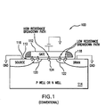
- FIG. 2 is a chart comparing fuse resistance with respect to width of the MOSFET anti-fuse device in FIG. 1 with at least one of the MOSFET antifuse devices in FIGs. 3-6 .
- FIG. 3 is a cross-section diagram illustrating a MOSFET anti-fuse device according to embodiments of the present invention.
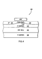
- FIG. 4 is a cross-section diagram illustrating a MOSFET anti-fuse device according to embodiments of the present invention.
- FIG. 7 is a flowchart illustrating a method to reduce on-state resistance and improving current characteristics of the MOSFET anti-fuse device, in according to embodiments of the present invention.
- anti-fuse and the terms storage or programmable coupled with the terms cell, element, or device are often used interchangeably in this field.
- the present invention is applicable to all these terms as they are generally understood in the relevant art.
- chip integrated circuit
- monolithic device semiconductor device and microelectronic device are often used interchangeably in this field.
- present invention is applicable to all of these terns as they are generally understood in the field.
- metal line trace, wire, conductor, signal path and signaling medium are all related. These related terms are generally interchangeable and appear in order from most specific to most general. In this field, metal lines are sometimes referred to as traces, wires, lines, interconnect or simply metal.
- Metal lines generally aluminum (Al) or an alloy of Al and copper (Cu), are conductors which provide signal paths for coupling, or interconnecting, electrical circuitry. Conductors other than metal are available in microelectronic devices.
- An anti-fuse may be formed from a conventional metal oxide semiconductor field effect transistor (MOSFET), which includes a high impedance between a gate and a source, a drain, a substrate, or a well. Gate oxide over the substrate can become a resistive short by applying a sufficient voltage, and causing part of the gate oxide to form current paths by diffusion of polysilicon gate material or silicon from the substrate.
- MOSFETs can be used as an anti-fuse structure by utilizing the gate oxide as a fusing element.
- the source and drain extension regions 120 and 122 generally have a lower concentration of dopants compared to the source and drain regions 116 and 118. However, the regions 116, 118, 120 and 122 can be doped to the same levels.
- the region in the substrate directly below the gate 112, and between source and drain extension regions 120 and 122, is typically referred to as a channel region 124.
- Resistive current paths can be formed between the gate 112, the channel region 124, or the source and drain extension regions 120, 122.
- the lowest resistance paths tend to be between the gate 112 and the source or drain regions 116,118 and the source or drain extension regions 120,122.
- the resistive current paths are formed from the gate electrode 112 to the substrate 114, which can comprise a P-well or N-well, the fuse resistance is much higher. Examples of this are taught in Robin Degraeve, et al., "Relation Between Breakdown Mode and Location in Short-Channel nMOSFETs and its Impact on Reliability Specifications," in Symposium on VLSI Technology Digest of Technical Papers (June 2001), and B.
- the soft breakdowns are undesirable because fuse resistance distribution is considerably higher than that of the hard breakdown.
- the fuse resistance of the conventional MOSFET anti-fuse device initially decreases with width, but begins to increase with a further decrease in width for a given power supply applied to the anti-fuse.
- the variability of the fuse resistance increases with a decrease in width.
- the fuse structure should be as small as possible.
- conventional MOSFET anti-fuse devices are not suitable to provide for a small structure of a high density memory cell, redundancy, or error correction due to variability of the fuse resistance and increase in fuse resistance.
- the present invention is directed to a device and associated manufacturing method that overcome these above-noted deficiencies in conventional MOSFET anti-fuses.
- FIG. 4 illustrates a MOSFET anti-fuse device 400 according to embodiments of the present invention.
- This embodiment is similar to FIG. 3, but includes a deep N-well region 402, which is formed within the lightly doped P-type substrate 330 beneath the source and drain regions 316, 318 and the channel 340.
- Ldd refers to "lightly doped drain," although both the source and drain contain the same label.
- the N or P before the Ldd refers to the type of doping. Although not shown, all the regions can have opposite dopants.
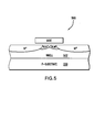
- FIG. 5 illustrates a MOSFET anti-fuse device 500 according to embodiments of the present invention. This embodiment is similar to FIG. 3, but includes an N-well 502 formed of an epitaxial layer on a lightly doped P-type substrate 330.
- FIG. 6 illustrates a MOSFET anti-fuse device 600 according embodiments of the present invention.
- This embodiment is similar to FIG. 3, but source and drain regions 616 and 618, source/drain extension regions 620 and 622, well region P-well, and the substrate are all of the same conductivity type (e.g., P-type).
- the substrate can be either a P-type substrate or a lightly-doped P-type substrate. In alternative embodiments, although not shown, the regions could all be doped with N-type materials.
- the programming is performed by application of power to the gate and at least one of the source region and the drain region to break down the gate oxide minimizing resistance between the gate and the channel.
- a deep N-well region is formed within the substrate beneath the source and drain regions and the channel.
- the source and drain regions are formed in anN-well layer that is formed on the substrate, which is doped with P type material.
- the lightly doped source and drain extension regions are formed completely under the gate to form an overlap region within the channel.
Landscapes
- Design And Manufacture Of Integrated Circuits (AREA)
Abstract
Description
Claims (20)
- An anti-fuse device, comprising:wherein programming of the anti-fuse is performed by application of power to said gate and one of said source region and said drain region to breakdown said gate oxide, which minimizes resistance between said gate and said channel.a substrate including,a source region laterally spaced from a drain region having a channel there between,a gate oxide formed on said channel,a gate formed on said gate oxide, andlightly doped source and drain extension regions formed in said channel and extending across said channel from said source and said drain regions, respectively, occupying a substantial portion of said channel,
- The anti-fuse device as recited in claim 1, wherein said power impresses a voltage on said gate and said at least one of said source region and said drain region.
- The anti-fuse device according to claim 1, wherein said source and drain regions receive a same amount of voltage during said programming.
- The anti-fuse device as recited in claim 1, wherein said source and drain regions are heavily doped with N-type material.
- The anti-fuse device as recited in claim 1, wherein said source and drain regions are heavily doped with P-type material.
- The anti-fuse device according to claim 1, further comprising:a deep N-well region formed within said substrate beneath said source region, said drain region, and said channel.
- The anti-fuse device according to claim 1, wherein said source region and said drain region are formed in an N-well layer that is formed on said substrate and wherein said substrate is doped with P-type material.
- The anti-fuse device according to claim 1, wherein said substrate is formed of lightly doped P-type material.
- The anti-fuse device as recited in claim 1, wherein said lightly doped source and drain extension regions overlap under said gate to form an overlap region within said channel.
- A method to reduce on-state resistance and improve current characteristics of an anti-fuse device, the method comprising the steps of:wherein said programming is performed by application of power to the gate and one of the source region and the drain region, which breaks down the gate oxide and minimizes resistance between the gate and the channel.providing a substrate;forming a channel between a source region laterally spaced from a drain region in said substrate;forming a gate oxide on the channel;forming a gate on the gate oxide;forming lightly doped source and drain extension regions in the channel, the lightly doped source and drain extension regions extending across the channel and occupying a substantial portion of the channel; andforming contacts to permit programming of the anti-fuse device,
- The method of claim 10, wherein said providing a substrate step comprises the step of providing a lightly doped P-type substrate.
- The method of claim 10, further comprising the step of doping the source and drain regions with N-type material.
- The method of claim 10, further comprising the step of doping the lightly doped source and drain extension regions with N-type material.
- The method of claim 10, further comprising the step of doping the source and drain regions with P-type material.
- The method of claim 10, further comprising the step of doping the lightly doped source and drain extension regions with P-type material.
- The method of claim 10, further comprising the step of forming a deep N-well region formed within the substrate beneath the source and drain regions and the channel.
- The method of claim 10, further comprising the step of forming a deep P-well region formed within the substrate beneath the source and drain regions and the channel.
- The method of claim 10, further comprising the steps of:doping the substrate with P-type material; andforming the source and the drain regions in an N-well layer that is formed on the substrate.
- The method of claim 10, further comprising the step of forming and overlap region within the channel, wherein the overlap region includes the lightly doped source and drain extension regions.
- An anti-fuse device, comprising:a substrate including,a channel formed between laterally spaced source and drain regions that are formed in said substrate,a gate oxide formed on said channel,a gate formed on said gate oxide, andlightly doped source and drain extension regions formed in said channel and extending across said channel from said source and said drain regions, respectively, and occupying a substantial portion of said channel.
Applications Claiming Priority (2)
| Application Number | Priority Date | Filing Date | Title |
|---|---|---|---|
| US10/197,437 US6700176B2 (en) | 2002-07-18 | 2002-07-18 | MOSFET anti-fuse structure and method for making same |
| US197437 | 2002-07-18 |
Publications (1)
| Publication Number | Publication Date |
|---|---|
| EP1385211A1 true EP1385211A1 (en) | 2004-01-28 |
Family
ID=30000057
Family Applications (1)
| Application Number | Title | Priority Date | Filing Date |
|---|---|---|---|
| EP03016223A Withdrawn EP1385211A1 (en) | 2002-07-18 | 2003-07-17 | Mosfet anti-fuse structure and method for making same |
Country Status (2)
| Country | Link |
|---|---|
| US (3) | US6700176B2 (en) |
| EP (1) | EP1385211A1 (en) |
Cited By (1)
| Publication number | Priority date | Publication date | Assignee | Title |
|---|---|---|---|---|
| CN103579246A (en) * | 2012-08-02 | 2014-02-12 | 美格纳半导体有限公司 | Otp memory cell and fabricating method thereof |
Families Citing this family (58)
| Publication number | Priority date | Publication date | Assignee | Title |
|---|---|---|---|---|
| US6700176B2 (en) * | 2002-07-18 | 2004-03-02 | Broadcom Corporation | MOSFET anti-fuse structure and method for making same |
| US7009883B2 (en) * | 2003-02-27 | 2006-03-07 | Broadcom Corporation | Automatic programming time selection for one time programmable memory |
| US7323726B1 (en) * | 2003-09-09 | 2008-01-29 | Spansion Llc | Method and apparatus for coupling to a common line in an array |
| US7072210B2 (en) * | 2004-04-26 | 2006-07-04 | Applied Intellectual Properties Co., Ltd. | Memory array |
| US7457154B2 (en) * | 2004-03-15 | 2008-11-25 | Applied Intellectual Properties Co., Ltd. | High density memory array system |
| US8735297B2 (en) | 2004-05-06 | 2014-05-27 | Sidense Corporation | Reverse optical proximity correction method |
| US9123572B2 (en) | 2004-05-06 | 2015-09-01 | Sidense Corporation | Anti-fuse memory cell |
| US7755162B2 (en) | 2004-05-06 | 2010-07-13 | Sidense Corp. | Anti-fuse memory cell |
| WO2005109516A1 (en) * | 2004-05-06 | 2005-11-17 | Sidense Corp. | Split-channel antifuse array architecture |
| US7511982B2 (en) * | 2004-05-06 | 2009-03-31 | Sidense Corp. | High speed OTP sensing scheme |
| US8767433B2 (en) | 2004-05-06 | 2014-07-01 | Sidense Corp. | Methods for testing unprogrammed OTP memory |
| US7161213B2 (en) | 2004-08-05 | 2007-01-09 | Broadcom Corporation | Low threshold voltage PMOS apparatus and method of fabricating the same |
| US7136303B2 (en) * | 2004-08-31 | 2006-11-14 | Broadcom Corporation | System and method using a one-time programmable memory cell |
| US7795094B2 (en) * | 2004-09-02 | 2010-09-14 | Micron Technology, Inc. | Recessed gate dielectric antifuse |
| US8160244B2 (en) * | 2004-10-01 | 2012-04-17 | Broadcom Corporation | Stateless hardware security module |
| US20060072748A1 (en) * | 2004-10-01 | 2006-04-06 | Mark Buer | CMOS-based stateless hardware security module |
| US8166296B2 (en) * | 2004-10-20 | 2012-04-24 | Broadcom Corporation | User authentication system |
| US8584200B2 (en) * | 2004-10-22 | 2013-11-12 | Broadcom Corporation | Multiple time outs for applications in a mobile device |
| US8027665B2 (en) * | 2004-10-22 | 2011-09-27 | Broadcom Corporation | System and method for protecting data in a synchronized environment |
| US7860486B2 (en) * | 2004-10-22 | 2010-12-28 | Broadcom Corporation | Key revocation in a mobile device |
| JP4772328B2 (en) * | 2005-01-13 | 2011-09-14 | 株式会社東芝 | Nonvolatile semiconductor memory device |
| KR100585629B1 (en) * | 2005-02-04 | 2006-06-07 | 삼성전자주식회사 | Anti-fuse circuit for improving reliability and anti-fusing method using same |
| US20070013026A1 (en) * | 2005-07-12 | 2007-01-18 | Ching-Hung Kao | Varactor structure and method for fabricating the same |
| KR100731141B1 (en) * | 2005-12-29 | 2007-06-22 | 동부일렉트로닉스 주식회사 | Semiconductor device and manufacturing method thereof |
| US20070210415A1 (en) * | 2006-03-07 | 2007-09-13 | Ping-Chang Wu | Anti-fuse and programming method of the same |
| US7485528B2 (en) * | 2006-07-14 | 2009-02-03 | Micron Technology, Inc. | Method of forming memory devices by performing halogen ion implantation and diffusion processes |
| US20080246080A1 (en) * | 2006-07-28 | 2008-10-09 | Broadcom Corporation | Shallow trench isolation (STI) based laterally diffused metal oxide semiconductor (LDMOS) |
| US7855414B2 (en) * | 2006-07-28 | 2010-12-21 | Broadcom Corporation | Semiconductor device with increased breakdown voltage |
| US20080036033A1 (en) * | 2006-08-10 | 2008-02-14 | Broadcom Corporation | One-time programmable memory |
| KR100866960B1 (en) * | 2007-02-16 | 2008-11-05 | 삼성전자주식회사 | Semiconductor integrated circuit |
| US20080211060A1 (en) * | 2007-03-01 | 2008-09-04 | Kuang-Yeh Chang | Anti-fuse which will not generate a non-linear current after being blown and otp memory cell utilizing the anti-fuse |
| US20090026576A1 (en) * | 2007-07-24 | 2009-01-29 | United Microelectronics Corp. | Anti-fuse |
| JP5666078B2 (en) * | 2007-07-27 | 2015-02-12 | ピーエスフォー ルクスコ エスエイアールエルPS4 Luxco S.a.r.l. | Antifuse element and semiconductor device having the same |
| JP2009054662A (en) * | 2007-08-24 | 2009-03-12 | Elpida Memory Inc | Antifuse element and semiconductor device having the same |
| JP2009267229A (en) * | 2008-04-28 | 2009-11-12 | Elpida Memory Inc | Semiconductor device and method for manufacturing same |
| US8049299B2 (en) | 2009-02-25 | 2011-11-01 | Freescale Semiconductor, Inc. | Antifuses with curved breakdown regions |
| US8203188B2 (en) * | 2009-05-22 | 2012-06-19 | Broadcom Corporation | Split gate oxides for a laterally diffused metal oxide semiconductor (LDMOS) |
| US20100295126A1 (en) * | 2009-05-22 | 2010-11-25 | Broadcom Corporation | High dielectric constant gate oxides for a laterally diffused metal oxide semiconductor (LDMOS) |
| US20110108926A1 (en) * | 2009-11-12 | 2011-05-12 | National Semiconductor Corporation | Gated anti-fuse in CMOS process |
| JP5523072B2 (en) * | 2009-12-02 | 2014-06-18 | ルネサスエレクトロニクス株式会社 | Antifuse element programming method and semiconductor device |
| US8274114B2 (en) * | 2010-01-14 | 2012-09-25 | Broadcom Corporation | Semiconductor device having a modified shallow trench isolation (STI) region and a modified well region |
| US8283722B2 (en) | 2010-06-14 | 2012-10-09 | Broadcom Corporation | Semiconductor device having an enhanced well region |
| US9123807B2 (en) | 2010-12-28 | 2015-09-01 | Broadcom Corporation | Reduction of parasitic capacitance in a semiconductor device |
| JP2012146817A (en) * | 2011-01-12 | 2012-08-02 | Toshiba Corp | Semiconductor device and method of manufacturing the same |
| JP2014053374A (en) * | 2012-09-05 | 2014-03-20 | Toshiba Corp | Semiconductor integrated circuit |
| US9184287B2 (en) | 2013-01-14 | 2015-11-10 | Broadcom Corporation | Native PMOS device with low threshold voltage and high drive current and method of fabricating the same |
| TWI503824B (en) * | 2013-09-13 | 2015-10-11 | 林崇榮 | Memory array and its non-volatile memory device |
| KR102173038B1 (en) * | 2013-11-26 | 2020-11-02 | 에스케이하이닉스 주식회사 | Anti-fuse of semiconductor device and method for fabricating the same |
| EP3183751A4 (en) * | 2014-08-19 | 2018-03-28 | Intel Corporation | Mos antifuse with void-accelerated breakdown |
| KR101678619B1 (en) * | 2015-04-27 | 2016-11-22 | 한국과학기술원 | Hardware based security apparatus and securiy method using the same |
| US10032783B2 (en) * | 2015-10-30 | 2018-07-24 | Globalfoundries Singapore Pte. Ltd. | Integrated circuits having an anti-fuse device and methods of forming the same |
| CN110931565B (en) * | 2018-09-19 | 2024-07-12 | 长鑫存储技术有限公司 | Transistor device with electrostatic protection capability and manufacturing method thereof |
| CN110537259A (en) * | 2019-06-28 | 2019-12-03 | 长江存储科技有限责任公司 | In-Memory Computing in 3D Memory Devices |
| CN110476209B (en) | 2019-06-28 | 2020-11-17 | 长江存储科技有限责任公司 | In-memory computation in three-dimensional memory devices |
| CN112420663B (en) * | 2019-08-23 | 2022-05-10 | 长鑫存储技术有限公司 | Antifuse structure and method of making the same |
| CN115811882A (en) | 2021-09-14 | 2023-03-17 | 联华电子股份有限公司 | semiconductor structure |
| US12272413B2 (en) * | 2022-06-13 | 2025-04-08 | Nanya Technology Corporation | Method of manufacturing an electrically programmable semiconductor anti-fuse device that includes utilizing previously fabricated device elements as masks for subsequently fabricated elements |
| US12315578B2 (en) | 2022-06-13 | 2025-05-27 | Nanya Technology Corporation | Semiconductor device with programmable feature |
Citations (4)
| Publication number | Priority date | Publication date | Assignee | Title |
|---|---|---|---|---|
| EP0495317A1 (en) * | 1991-01-18 | 1992-07-22 | Actel Corporation | Low voltage programmable antifuse and method for programming same |
| US20010050407A1 (en) * | 2000-06-08 | 2001-12-13 | Tito Gelsomini | Anti-fuse structure and method of writing and reading in integrated circuits |
| US6388305B1 (en) * | 1999-12-17 | 2002-05-14 | International Business Machines Corporation | Electrically programmable antifuses and methods for forming the same |
| US20020074616A1 (en) * | 2000-12-20 | 2002-06-20 | Vincent Chen | System and method for one-time programmed memory through direct-tunneling oxide breakdown |
Family Cites Families (18)
| Publication number | Priority date | Publication date | Assignee | Title |
|---|---|---|---|---|
| US4397887A (en) * | 1982-08-18 | 1983-08-09 | National Semiconductor Corporation | Postponed ROM programming |
| US5237193A (en) * | 1988-06-24 | 1993-08-17 | Siliconix Incorporated | Lightly doped drain MOSFET with reduced on-resistance |
| US5619063A (en) | 1993-07-07 | 1997-04-08 | Actel Corporation | Edgeless, self-aligned, differential oxidation enhanced and difusion-controlled minimum-geometry antifuse and method of fabrication |
| US5633202A (en) * | 1994-09-30 | 1997-05-27 | Intel Corporation | High tensile nitride layer |
| US5672994A (en) * | 1995-12-21 | 1997-09-30 | International Business Machines Corporation | Antifuse circuit using standard MOSFET devices |
| US5742555A (en) * | 1996-08-20 | 1998-04-21 | Micron Technology, Inc. | Method of anti-fuse repair |
| JPH1084045A (en) * | 1996-09-06 | 1998-03-31 | Matsushita Electron Corp | Semiconductor integrated circuit device and method of manufacturing the same |
| US5909049A (en) | 1997-02-11 | 1999-06-01 | Actel Corporation | Antifuse programmed PROM cell |
| JP2000011684A (en) * | 1998-06-18 | 2000-01-14 | Mitsubishi Electric Corp | Input protection circuit, antifuse address detection circuit, and semiconductor integrated circuit device |
| JP3425100B2 (en) * | 1999-03-08 | 2003-07-07 | 松下電器産業株式会社 | Field programmable gate array and method of manufacturing the same |
| CN1170320C (en) * | 2000-03-13 | 2004-10-06 | 松下电器产业株式会社 | Semiconductor device and manufacturing method thereof |
| US6266269B1 (en) * | 2000-06-07 | 2001-07-24 | Xilinx, Inc. | Three terminal non-volatile memory element |
| US6525955B1 (en) * | 2001-12-18 | 2003-02-25 | Broadcom Corporation | Memory cell with fuse element |
| US6704236B2 (en) * | 2002-01-03 | 2004-03-09 | Broadcom Corporation | Method and apparatus for verification of a gate oxide fuse element |
| US6693819B2 (en) * | 2002-01-08 | 2004-02-17 | Broadcom Corporation | High voltage switch circuitry |
| US6606262B2 (en) | 2002-01-10 | 2003-08-12 | Hewlett-Packard Development Company, L.P. | Magnetoresistive random access memory (MRAM) with on-chip automatic determination of optimized write current method and apparatus |
| US6518614B1 (en) * | 2002-02-19 | 2003-02-11 | International Business Machines Corporation | Embedded one-time programmable non-volatile memory using prompt shift device |
| US6700176B2 (en) | 2002-07-18 | 2004-03-02 | Broadcom Corporation | MOSFET anti-fuse structure and method for making same |
-
2002
- 2002-07-18 US US10/197,437 patent/US6700176B2/en not_active Expired - Lifetime
-
2003
- 2003-07-17 EP EP03016223A patent/EP1385211A1/en not_active Withdrawn
-
2004
- 2004-02-09 US US10/773,263 patent/US6902958B2/en not_active Expired - Lifetime
-
2005
- 2005-03-31 US US11/094,269 patent/US7897967B2/en not_active Expired - Fee Related
Patent Citations (4)
| Publication number | Priority date | Publication date | Assignee | Title |
|---|---|---|---|---|
| EP0495317A1 (en) * | 1991-01-18 | 1992-07-22 | Actel Corporation | Low voltage programmable antifuse and method for programming same |
| US6388305B1 (en) * | 1999-12-17 | 2002-05-14 | International Business Machines Corporation | Electrically programmable antifuses and methods for forming the same |
| US20010050407A1 (en) * | 2000-06-08 | 2001-12-13 | Tito Gelsomini | Anti-fuse structure and method of writing and reading in integrated circuits |
| US20020074616A1 (en) * | 2000-12-20 | 2002-06-20 | Vincent Chen | System and method for one-time programmed memory through direct-tunneling oxide breakdown |
Cited By (2)
| Publication number | Priority date | Publication date | Assignee | Title |
|---|---|---|---|---|
| CN103579246A (en) * | 2012-08-02 | 2014-02-12 | 美格纳半导体有限公司 | Otp memory cell and fabricating method thereof |
| CN103579246B (en) * | 2012-08-02 | 2018-03-27 | 美格纳半导体有限公司 | One-time programmable memory cell and its manufacture method |
Also Published As
| Publication number | Publication date |
|---|---|
| US20050258482A1 (en) | 2005-11-24 |
| US20040157379A1 (en) | 2004-08-12 |
| US6700176B2 (en) | 2004-03-02 |
| US20040023440A1 (en) | 2004-02-05 |
| US7897967B2 (en) | 2011-03-01 |
| US6902958B2 (en) | 2005-06-07 |
Similar Documents
| Publication | Publication Date | Title |
|---|---|---|
| US6700176B2 (en) | MOSFET anti-fuse structure and method for making same | |
| US8076673B2 (en) | Recessed gate dielectric antifuse | |
| EP1743380B1 (en) | Split-channel antifuse array architecture | |
| US7102951B2 (en) | OTP antifuse cell and cell array | |
| US6913954B2 (en) | Programmable fuse device | |
| US6804159B2 (en) | Semiconductor device having fuse and its manufacture method | |
| US6960819B2 (en) | System and method for one-time programmed memory through direct-tunneling oxide breakdown | |
| US6855586B2 (en) | Low voltage breakdown element for ESD trigger device | |
| TW201230050A (en) | Electronics system, anti-fuse memory and method for the same | |
| US9214466B2 (en) | Method and system for split threshold voltage programmable bitcells | |
| WO2014081984A1 (en) | Integrated circuit device and method for making same | |
| US20080036033A1 (en) | One-time programmable memory | |
| US8470645B2 (en) | Method for manufacturing an antifuse memory cell | |
| US7531886B2 (en) | MOSFET fuse programmed by electromigration | |
| US20050067670A1 (en) | Method and apparatus for using cobalt silicided polycrystalline silicon for a one time programmable non-volatile semiconductor memory | |
| US20060157819A1 (en) | Efuse structure | |
| US20030062594A1 (en) | Anti-fuse structure with low on-state resistance and low off-state leakage | |
| US7772063B2 (en) | Reduced-step CMOS processes for low-cost radio frequency identification devices | |
| US20210351192A1 (en) | One-time programmable device with antifuse | |
| US20260040538A1 (en) | One-time programmable memory cell | |
| US7518167B2 (en) | Semiconductor device | |
| KR20000051373A (en) | Electric fuse for using memory chip |
Legal Events
| Date | Code | Title | Description |
|---|---|---|---|
| PUAI | Public reference made under article 153(3) epc to a published international application that has entered the european phase |
Free format text: ORIGINAL CODE: 0009012 |
|
| AK | Designated contracting states |
Kind code of ref document: A1 Designated state(s): AT BE BG CH CY CZ DE DK EE ES FI FR GB GR HU IE IT LI LU MC NL PT RO SE SI SK TR |
|
| AX | Request for extension of the european patent |
Extension state: AL LT LV MK |
|
| 17P | Request for examination filed |
Effective date: 20040728 |
|
| AKX | Designation fees paid |
Designated state(s): DE FR GB |
|
| RAP1 | Party data changed (applicant data changed or rights of an application transferred) |
Owner name: BROADCOM CORPORATION |
|
| GRAP | Despatch of communication of intention to grant a patent |
Free format text: ORIGINAL CODE: EPIDOSNIGR1 |
|
| RIC1 | Information provided on ipc code assigned before grant |
Ipc: H01L 23/525 20060101ALI20160617BHEP Ipc: H01L 29/78 20060101ALI20160617BHEP Ipc: H01L 29/66 20060101ALI20160617BHEP Ipc: H01L 27/112 20060101AFI20160617BHEP |
|
| INTG | Intention to grant announced |
Effective date: 20160718 |
|
| STAA | Information on the status of an ep patent application or granted ep patent |
Free format text: STATUS: THE APPLICATION IS DEEMED TO BE WITHDRAWN |
|
| 18D | Application deemed to be withdrawn |
Effective date: 20161129 |