EP1385171A2 - Method for recording in a nonvolatile solid-state magnetic memory - Google Patents
Method for recording in a nonvolatile solid-state magnetic memory Download PDFInfo
- Publication number
- EP1385171A2 EP1385171A2 EP03016351A EP03016351A EP1385171A2 EP 1385171 A2 EP1385171 A2 EP 1385171A2 EP 03016351 A EP03016351 A EP 03016351A EP 03016351 A EP03016351 A EP 03016351A EP 1385171 A2 EP1385171 A2 EP 1385171A2
- Authority
- EP
- European Patent Office
- Prior art keywords
- recording
- recording layer
- electric field
- layer
- nonvolatile solid
- Prior art date
- Legal status (The legal status is an assumption and is not a legal conclusion. Google has not performed a legal analysis and makes no representation as to the accuracy of the status listed.)
- Withdrawn
Links
Images


Classifications
-
- G—PHYSICS
- G11—INFORMATION STORAGE
- G11C—STATIC STORES
- G11C11/00—Digital stores characterised by the use of particular electric or magnetic storage elements; Storage elements therefor
- G11C11/02—Digital stores characterised by the use of particular electric or magnetic storage elements; Storage elements therefor using magnetic elements
- G11C11/14—Digital stores characterised by the use of particular electric or magnetic storage elements; Storage elements therefor using magnetic elements using thin-film elements
- G11C11/15—Digital stores characterised by the use of particular electric or magnetic storage elements; Storage elements therefor using magnetic elements using thin-film elements using multiple magnetic layers
-
- G—PHYSICS
- G11—INFORMATION STORAGE
- G11C—STATIC STORES
- G11C11/00—Digital stores characterised by the use of particular electric or magnetic storage elements; Storage elements therefor
- G11C11/02—Digital stores characterised by the use of particular electric or magnetic storage elements; Storage elements therefor using magnetic elements
- G11C11/14—Digital stores characterised by the use of particular electric or magnetic storage elements; Storage elements therefor using magnetic elements using thin-film elements
Definitions
- This invention relates to a method for recording in a nonvolatile solid-state magnetic memory.
- nonvolatile solid-state magnetic memory having a ferromagnetic layer as a recording layer, it is required for recording to apply a given external magnetic field to the recording layer.
- the miniaturization causes the enhancement of the demagnetizing field in the recording layer, so that conventionally, it is required for recording in the nonvolatile solid-state magnetic memory to apply to the memory an external magnetic field large enough to invert the magnetization of the recording layer against the large demagnetizing field thereof.
- a large electric power consumption is required, and thus, the nonvolatile solid-state magnetic memory practically usable and of low electric power consumption was able to be provided.
- this invention relates to a method for recording in a nonvolatile solid-state magnetic field with a recording layer made of carrier induced ferromagnetic material, comprising the steps of:
- the carrier induced ferromagnetic material is one of new ferromagnetic semiconductors, and can control the magnetic property thereof by adjusting the carrier number and the carrier spin polarization by means of light or electric field.
- the inventors have conceived to utilize the carrier induced ferromagnetic material as a recording layer of a nonvolatile solid-state magnetic memory. In this case, by applying to the recording layer a first electric field and a second electric field satisfying the above-mentioned requirement under a given magnetic field, the magnetization of the recording layer can be inverted. In other words, the magnetization of the recording layer can be inverted by switching to the second electric field from the first electric field.
- the recording performance for a nonvolatile solid-state magnetic memory can be done, so that the nonvolatile solid-state magnetic memory practically usable and of low electric power consumption can be provided.
- the magnitude of the magnetization of the recording layer can be increased and decreased to be inverted alternately and successively. Therefore, if information is stored in the recording layer of the nonvolatile solid-state magnetic memory on the direction of the magnetization of the recording layer, the recording performance for the nonvolatile solid-state magnetic memory can be done successively.
- the recording layer is formed above a substrate, and a metallic electrode layer is formed above the recording layer via an insulating layer, thereby to complete an electric field effect transistor.
- the recording layer functions as a channel layer
- the metallic electrode layer functions as a gate electrode. Therefore, the electric field for the reduction of the coercive force of the recording layer can be applied to the nonvolatile solid-state magnetic memory via the metallic electrode layer, and then, the recording operation for the nonvolatile solid-state magnetic memory can be simplified.
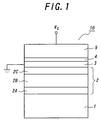
- Fig. 1 is a structural view showing a nonvolatile solid-state magnetic memory to be recorded according to the present invention.
- the nonvolatile solid-state magnetic memory 10 illustrated in Fig. 1 on a given substrate 1 are formed successively a buffer layer 2, a recording layer 3 made of carrier induced ferromagnetic material, and a metallic electrode layer 5 via an insulating layer 4, thereby to complete an electric field effect transistor.
- the carrier induced ferromagnetic material forming the recording layer 3 is ferromagnetic semiconductor such as (Ga, Mn)As or (In, Mn)As, which has excellent ferromagnetic semiconductor properties and whereby the recording operation for the nonvolatile solid-state magnetic memory according to the present invention can be performed in good condition and the recording information can be retained stably for a long time.
- ferromagnetic semiconductor such as (Ga, Mn)As or (In, Mn)As
- the thickness of the recording layer 3 is preferably set within 0.3-200nm, particularly within 3-10nm.
- the nonvolatile solid-state magnetic memory can be sufficiently miniaturized under the recording performance in good condition and the stable retention of the recording information.
- the substrate 1 is preferably made of GaAs single crystal.
- the recording layer 3 can be epitaxially grown in good crystallinity, to enhance the performance of the nonvolatile solid-state magnetic memory 10.
- the buffer layer 3 is constructed of a multilayered structure composed of semiconductor layers 2A-2C.
- the difference in lattice constant between the substrate 1 and the recording layer 3 can be compensated effectively, to enhance the epitaxial growth of the recording layer 3 and thus, develop the performance of the nonvolatile solid-state magnetic memory 10 effectively and efficiently.
- the multilayered buffer layer can be preferably employed when the recording layer 3 is made of (In, Mn)As and the substrate 1 is made of (001)GaAs single crystal. Since the mismatch in lattice constant between the (In, Mn)As and the (001)GaAs single crystal is about 7%, the use of the multilayered buffer layer can compensate the mismatch in lattice constant and thus, prompt the eptitaxial growth of the recording layer 3.
- the semiconductor layer 2A is made of AlSb layer
- the semiconductor layer 2b is made of AlGaSb layer
- the semiconductor layer 2c is made of InAs layer.
- the insulating layer 4 may be made of an inorganic material such as SiO 2 , SiN, Al 2 O 3 or an organic material such as polyimide.
- the metallic electrode layer 5 may be made of conductive metallic material such as Al or Au.
- the nonvolatile solid-state magnetic memory 10 is so constructed as the electric field effect transistor, the metallic electrode layer 5 functions as a gate electrode and the recording layer 3 functions as a channel layer.
- Fig. 2 is an explanatory view showing the principle of the recording method of the present invention.
- the direction of the magnetization of the recording layer 3 is designated by the arrow.
- a given external magnetic field B 0 is applied to the recording layer 3 of the nonvolatile solid-state magnetic memory 10, to be initialized, e.g., by upward alignment of the magnetization while a given electric field is applied to the recording layer 3 so as to reduce the hole carrier concentration of the recording layer 3.
- the magnetization of the recording layer 3 can be inverted by the external magnetic field B 0 with relatively small intensity.
- the application periods of time of the first electric field and the second electric field can be adjusted on the sort and the configuration of the nonvolatile solid-state magnetic memory 10, but preferably set within a range of several ns to several ⁇ s.
- the magnetization of the recording layer 3 can be inverted successively, so that if information is stored in the recording layer 3 on the direction of the magnetization of the recording layer 3, the recording operation can be carried out successively.
- the coercive forces of the recording layer 3 are set to "H1" and "H2" at the application of the first electric field E1 and the second electric field E2, respectively, the relation of "H1>H2" is satisfied because the hole carrier concentration of the recording layer 3 is decreased by the second electric field E2. Therefore, the recording operation for the recording layer 3 can be performed in good condition only if the magnetic field B is applied so as to satisfy the relation of "H1>B>H2". However, it is not always required to satisfy the above relation of the intensity of the magnetic field B.
- the intensities of the first electric field and the second electric field are not restricted only if the recording operation can be performed on the recording principle as shown in Fig. 2.
- the intensity of the first electric field is set within 0-10MV/cm
- the intensity of the second electric field is set within 0-0.01MV/cm.
- the absolute intensity of the second electric field E2 is set larger than that of the first electric field E1. In this case, the recording operation can be performed in good condition, irrespective of the thickness of the recording layer 3 and the like.
- a nonvolatile solid-state magnetic memory as shown in Fig. 1 was fabricated.
- a (001)GaAs single crystal substrate was employed, and heated to 550°C.
- an AlAs layer and an Al 0.82 Ga 0.18 Sb layer were successively formed in thicknesses of 50nm and 300nm, respectively on the substrate by means of MBE.
- the substrate was cooled down to 450°C, and an InAs layer was formed in a thickness of 5nm by means of MBE, to complete a buffer layer.
- the substrate was cooled down to 250°C, and an (In 0.967 Mn 0.033 )As layer as a recording layer was formed in a thickness of 4nm by means of MBE.
- an SiO 2 insulating layer was formed in a thickness of 0.9 ⁇ m by means of spin coating, and a Cr(5nm)/Au(95nm) as a metallic electrode layer was formed by means of deposition, thereby to complete an intended nonvolatile solid-state magnetic memory.
- Fig. 3 is a graph showing the variation in Hall resistance R Hall of the recording layer at 32K.
- an electric field of -1.5MV/cm was applied to the (In 0.967 Mn 0.033 )As recording layer to be initialized via the Cr/Au electrode layer under a magnetic field of 5mT.
- a recording method for a new nonvolatile solid-state magnetic memory practically usable and of low electric consumption can be provided.
Landscapes
- Engineering & Computer Science (AREA)
- Computer Hardware Design (AREA)
- Semiconductor Memories (AREA)
- Mram Or Spin Memory Techniques (AREA)
- Hall/Mr Elements (AREA)
Abstract
Description
and
Claims (10)
- A method for recording in a nonvolatile solid-state magnetic field with a recording layer made of carrier induced ferromagnetic material, comprising the steps of:applying a given magnetic field to said recording layerapplying a first electric field to said recording layer under said magnetic field,
andapplying a second electric field to said recording layer under said magnetic field so that a hole carrier concentration of said recording layer is reduced lower than at the application of said first electric field, to invert a magnetization of said recording layer and thus, realize recording operation for said recording layer. - The recording method as defined in claim 1, wherein said first electric field and said second electric field are applied alternately to said recording layer, to invert said magnetization of said recording layer alternately, and thus, realize successive recording operation for said recording layer.
- The recording method as defined in claim 1 or 2, wherein an intensity of said magnetic field is set within a coercive force range of said recording layer during the application of said first electric field and said second electric field.
- he recording method as defined in any one of claims 1-3, wherein said carrier induced ferromagnetic material is carrier induced ferromagnetic semiconductor.
- The recording method as defined in claim 4, wherein said carrier induced ferromagnetic semiconductor is at least one of (Ga, Mn)As and (In, Mn)As.
- The recording method as defined in any one of claims 1-5, wherein a thickness of said recording layer is set within 0.3-200nm.
- The recording method as defined in any one of claims 1-6, wherein an absolute intensity of said first electric field is set within 0-10MV/cm and an absolute intensity of said second electric field is set larger than said absolute intensity of said first electric field.
- The recording method as defined in any one of claims 1-7, wherein said nonvolatile solid-state magnetic memory includes a given substrate to support said recording layer and a metallic electrode layer provided above said recording layer via an insulating layer, thereby to complete an electric field effect transistor, and said recording layer functions as a channel layer and said metallic electrode layer functions as a gate electrode, whereby said first electric field and said electric field are applied to said recording layer via said metallic electrode layer.
- The recording method as defined in claim 8, wherein said nonvolatile solid-state magnetic memory includes a buffer layer between said substrate and said recording layer.
- The recording method as defined in any one of claims 5-9, wherein said substrate is made of GaAs.
Applications Claiming Priority (2)
| Application Number | Priority Date | Filing Date | Title |
|---|---|---|---|
| JP2002212003 | 2002-07-22 | ||
| JP2002212003A JP3932356B2 (en) | 2002-07-22 | 2002-07-22 | Recording method for nonvolatile solid-state magnetic memory |
Publications (2)
| Publication Number | Publication Date |
|---|---|
| EP1385171A2 true EP1385171A2 (en) | 2004-01-28 |
| EP1385171A3 EP1385171A3 (en) | 2004-08-11 |
Family
ID=29997206
Family Applications (1)
| Application Number | Title | Priority Date | Filing Date |
|---|---|---|---|
| EP03016351A Withdrawn EP1385171A3 (en) | 2002-07-22 | 2003-07-18 | Method for recording in a nonvolatile solid-state magnetic memory |
Country Status (5)
| Country | Link |
|---|---|
| US (1) | US20040085811A1 (en) |
| EP (1) | EP1385171A3 (en) |
| JP (1) | JP3932356B2 (en) |
| KR (1) | KR20040010274A (en) |
| TW (1) | TW200405340A (en) |
Families Citing this family (4)
| Publication number | Priority date | Publication date | Assignee | Title |
|---|---|---|---|---|
| DE602006000836T2 (en) * | 2005-03-24 | 2009-05-14 | Hitachi, Ltd. | Line control arrangement |
| JP5119434B2 (en) * | 2006-09-01 | 2013-01-16 | 国立大学法人長岡技術科学大学 | Magnetic semiconductor thin film and method of manufacturing magnetic semiconductor thin film |
| EP2015307B8 (en) * | 2007-07-13 | 2013-05-15 | Hitachi Ltd. | Magnetoresistive device |
| US20170345831A1 (en) * | 2016-05-25 | 2017-11-30 | Micron Technology, Inc. | Ferroelectric Devices and Methods of Forming Ferroelectric Devices |
Family Cites Families (5)
| Publication number | Priority date | Publication date | Assignee | Title |
|---|---|---|---|---|
| EP0877398B1 (en) * | 1997-05-09 | 2003-12-17 | Kabushiki Kaisha Toshiba | Magnetic element and magnetic head and magnetic memory device using thereof |
| US6611405B1 (en) * | 1999-09-16 | 2003-08-26 | Kabushiki Kaisha Toshiba | Magnetoresistive element and magnetic memory device |
| JP3891540B2 (en) * | 1999-10-25 | 2007-03-14 | キヤノン株式会社 | Magnetoresistive memory, method for recording / reproducing information recorded in magnetoresistive memory, and MRAM |
| JP4300740B2 (en) * | 2001-03-21 | 2009-07-22 | セイコーエプソン株式会社 | Ferroelectric memory device and electronic device including the same |
| JP2003078147A (en) * | 2001-08-31 | 2003-03-14 | Canon Inc | Charge injection type spin transistor |
-
2002
- 2002-07-22 JP JP2002212003A patent/JP3932356B2/en not_active Expired - Lifetime
-
2003
- 2003-07-16 US US10/619,580 patent/US20040085811A1/en not_active Abandoned
- 2003-07-18 TW TW092119655A patent/TW200405340A/en unknown
- 2003-07-18 EP EP03016351A patent/EP1385171A3/en not_active Withdrawn
- 2003-07-21 KR KR1020030049626A patent/KR20040010274A/en not_active Ceased
Also Published As
| Publication number | Publication date |
|---|---|
| KR20040010274A (en) | 2004-01-31 |
| JP2004055867A (en) | 2004-02-19 |
| US20040085811A1 (en) | 2004-05-06 |
| EP1385171A3 (en) | 2004-08-11 |
| TW200405340A (en) | 2004-04-01 |
| JP3932356B2 (en) | 2007-06-20 |
Similar Documents
| Publication | Publication Date | Title |
|---|---|---|
| EP1764838B1 (en) | Use of a spin transistor, using a spin-orbit coupling induced magnetic field | |
| US7994555B2 (en) | Spin transistor using perpendicular magnetization | |
| Hirohata et al. | Roadmap for emerging materials for spintronic device applications | |
| US8748957B2 (en) | Coherent spin field effect transistor | |
| US6355953B1 (en) | Spintronic devices and method for injecting spin polarized electrical currents into semiconductors | |
| US11264476B2 (en) | Magnetic contacts for spin qubits | |
| KR20090062601A (en) | Spin Transistor Using Epitaxial Growth Ferromagnetic-Semiconductor Junction | |
| US20200212294A1 (en) | Electrically controlled nanomagnet and spin orbit torque magnetic random access memory including the same | |
| US20040085811A1 (en) | Method for recording in a nonvolatile solid-state magnetic memory | |
| US20100084633A1 (en) | Spin transistor using double carrier supply layer structure | |
| EP1385203A2 (en) | Nonvolatile solid-state magnetic memory, method for controlling coercive force of nonvolatile solid-state magnetic memory, and method for recording in nonvolatile solid-state magnetic memory | |
| JP5248446B2 (en) | Electronic circuit | |
| JP2009059820A (en) | Spin transistor, and semiconductor memory | |
| US9620654B2 (en) | Coherent spin field effect transistor | |
| US7087971B2 (en) | Magnetic sensor based on efficient spin injection into semiconductors | |
| Petukhov et al. | Electron spin polarization in resonant interband tunneling devices | |
| JP2010073960A (en) | Semiconductor device | |
| KR20070048657A (en) | Tunnel junction barrier layer containing thin semiconductor with spin sensitivity | |
| US7790585B2 (en) | Antiferromagnetic half-metallic semiconductor and manufacturing method therefor | |
| Ono et al. | Ferromagnetic single electron transistor | |
| WO2008005719A2 (en) | Spin injector | |
| US20030197235A1 (en) | Conductive film layer for hall effect device | |
| Nozaki et al. | Material strategies for energy-efficient voltage-controlled magnetic tunnel junctions | |
| US7315041B2 (en) | Switching devices based on half-metals | |
| CN100459149C (en) | Conduction control device |
Legal Events
| Date | Code | Title | Description |
|---|---|---|---|
| PUAI | Public reference made under article 153(3) epc to a published international application that has entered the european phase |
Free format text: ORIGINAL CODE: 0009012 |
|
| 17P | Request for examination filed |
Effective date: 20030718 |
|
| AK | Designated contracting states |
Kind code of ref document: A2 Designated state(s): AT BE BG CH CY CZ DE DK EE ES FI FR GB GR HU IE IT LI LU MC NL PT RO SE SI SK TR |
|
| AX | Request for extension of the european patent |
Extension state: AL LT LV MK |
|
| PUAL | Search report despatched |
Free format text: ORIGINAL CODE: 0009013 |
|
| PUAF | Information related to the publication of a search report (a3 document) modified or deleted |
Free format text: ORIGINAL CODE: 0009199SEPU |
|
| STAA | Information on the status of an ep patent application or granted ep patent |
Free format text: STATUS: THE APPLICATION HAS BEEN WITHDRAWN |
|
| AK | Designated contracting states |
Kind code of ref document: A3 Designated state(s): AT BE BG CH CY CZ DE DK EE ES FI FR GB GR HU IE IT LI LU MC NL PT RO SE SI SK TR |
|
| AX | Request for extension of the european patent |
Extension state: AL LT LV MK |
|
| 18W | Application withdrawn |
Effective date: 20040624 |
|
| D17D | Deferred search report published (deleted) |