EP1385084A1 - Logarithmic transformer and method of logarithmic transformation - Google Patents

Logarithmic transformer and method of logarithmic transformation Download PDF

Info

Publication number
EP1385084A1
EP1385084A1 EP03016797A EP03016797A EP1385084A1 EP 1385084 A1 EP1385084 A1 EP 1385084A1 EP 03016797 A EP03016797 A EP 03016797A EP 03016797 A EP03016797 A EP 03016797A EP 1385084 A1 EP1385084 A1 EP 1385084A1
Authority
EP
European Patent Office
Prior art keywords
bit
bit string
bits
logarithmic
logic
Prior art date
Legal status (The legal status is an assumption and is not a legal conclusion. Google has not performed a legal analysis and makes no representation as to the accuracy of the status listed.)
Withdrawn
Application number
EP03016797A
Other languages
German (de)
French (fr)
Inventor
Yuji c/o Kawagoe Koujou Yamamoto
Current Assignee (The listed assignees may be inaccurate. Google has not performed a legal analysis and makes no representation or warranty as to the accuracy of the list.)
Pioneer Corp
Original Assignee
Pioneer Corp
Priority date (The priority date is an assumption and is not a legal conclusion. Google has not performed a legal analysis and makes no representation as to the accuracy of the date listed.)
Filing date
Publication date
Application filed by Pioneer Corp filed Critical Pioneer Corp
Publication of EP1385084A1 publication Critical patent/EP1385084A1/en
Withdrawn legal-status Critical Current

Links

Images

Classifications

    • GPHYSICS
    • G06COMPUTING OR CALCULATING; COUNTING
    • G06FELECTRIC DIGITAL DATA PROCESSING
    • G06F7/00Methods or arrangements for processing data by operating upon the order or content of the data handled
    • G06F7/38Methods or arrangements for performing computations using exclusively denominational number representation, e.g. using binary, ternary, decimal representation
    • G06F7/48Methods or arrangements for performing computations using exclusively denominational number representation, e.g. using binary, ternary, decimal representation using non-contact-making devices, e.g. tube, solid state device; using unspecified devices
    • G06F7/544Methods or arrangements for performing computations using exclusively denominational number representation, e.g. using binary, ternary, decimal representation using non-contact-making devices, e.g. tube, solid state device; using unspecified devices for evaluating functions by calculation
    • G06F7/556Logarithmic or exponential functions

Definitions

  • the invention relates to a logarithmic transformer and a method of logarithmic transformation for logarithmically transforming, for example, digital data or the like.
  • logarithmic transformation has widely been used as useful means in the field of digital signal processing.
  • Fig. 1A shows the configuration of a typical logarithmic transformer which has been known heretofore.
  • the logarithmic transformer is implemented as hardware for the sake of fast logarithmic transformation.
  • the logarithmic transformer includes an address decoder 1 which is a logic circuit and a logarithmic ROM 2 which is made of a read-only semiconductor memory.
  • the logarithmic ROM 2 is configured as a so-called look-up table, in which a number of pieces of logarithmic transformation data corresponding to digital data to be logarithmically transformed are stored in advance.
  • the address decoder 1 When the address decoder 1 receives digital data to be logarithmically transformed, it transforms (decodes) the digital data into address data to designate an address of the logarithmic ROM 2 so that logarithmic transformation data corresponding to the digital data is read out.
  • the values of digital data to be logarithmically transformed, the address data for designating addresses of the logarithmic ROM 2, and the logarithmic transformation data prestored at the addresses designated by the address data are determined in one-on-one correspondence.
  • the logarithmic transformation data corresponding to the digital data is output from the logarithmic ROM 2 as a result of logarithmic transformation, thereby allowing fast logarithmic transformation.
  • the conventional logarithmic transformer has had a problem of being extremely large in circuit scale.
  • the address decoder 1 shown in Fig. 1A is composed of a plurality of stages of logic circuits 1a and 16 as shown in Fig. 1B.
  • Each of the logic circuits 1a and 1b includes a number of logic operation elements (inverters, OR gates, NOR gates, AND gates, NAND gates, etc.) in combination.
  • the plurality of logic circuits 1a lying in the first stage are made of a plurality of inverters and NOR gates for creating intricate combinations of n-bit (n is an arbitrary natural number) input digital data for logic operation.
  • the logic circuit 1b in the next stage is also made of a plurality of logic operation elements so that a number of pieces of data output from the plurality of logic circuits 1a are intricately combined for logic operation.
  • the logic circuit 1b includes a number of stages of logic circuits, not a single stage alone.
  • the address decoder 1 has had a large circuit scale.
  • the look-up table configuration of the logarithmic ROM 2 has also contributed an increase in circuit scale.
  • the logarithmic ROM 2 must previously contain at least 2 n values of logarithmic transformation data according to the number of bits n of the digital data to be logarithmically transformed.
  • the logarithmic ROM 2 still requires a total memory capacity of at least 2 n ⁇ m bits.
  • the logarithmic ROM 2 has required a high memory capacity, contributing to the large circuit scale.
  • the present invention has been achieved in view of the conventional problems illustrated above. It is thus an object of the present invention to provide a logarithmic transformer having a new configuration.
  • a logarithmic transformer comprising: a first bit string generator for generating a first bit string of binary data indicating the position of a highest order bit of logic "1" out of bits of digital data to be logarithmically transformed; and a second bit string generator for determining, from the digital data, a second bit string of order lower than the highest order bit of logic "1", the logarithmic transformer outputting logarithmic transformation data, which includes the first bit string as an integral part of a logarithmic transformation value resulting from a logarithmic transformation of the digital data and the second bit string as a fractional part of the logarithmic transformation value.
  • the first bit string generator comprises: a detecting unit for detecting the position of the highest order bit of logic "1" out of the bits of the digital data; and a generating unit for generating the first bit string based on a result of detection by the detecting unit.
  • the detecting unit detects the highest order bit of logic "1" by decoding the digital data.
  • the generating unit contains pieces of binary data indicating the positions of the respective bits of the digital data, and selects one out of the pieces of binary data based on the result of detection by the detecting unit, thereby generating the binary data indicating the position of the highest order bit of logic "1.”
  • the generating unit is composed of a switching circuit for selecting one out of the pieces of binary data, based on the result of detection by the detecting unit.
  • the detecting unit comprises: a first logic circuit for outputting data for excluding a bit string lower than the highest order bit of logic "1" from the bits of the digital data; and a second logic circuit for removing the bit string excluded by the data from the bits of the digital data, thereby detecting the highest order bit of logic "1.”
  • the first logic circuit includes a plurality of OR gates for inputting respective bits of the digital data from a most significant bit to a least significant bit, the OR gates having their outputs and inputs cascaded in association with the most significant bit to the least significant bit; and the OR gates generate the data for excluding by performing OR operations between the outputs of the OR gates of higher order bits and the respective bits of the digital data.
  • the second logic circuit detects the highest order bit of logic "1" by performing AND operations between the respective bits of the digital data and the data for excluding.
  • the second bit string generator determines, as the second bit string, a bit string of a predetermined number of bits including a bit following the highest order bit of logic "1" out of the bits of the digital data.
  • the second bit string generator when the number of bits from the bit following the highest order bit to a least significant bit of the digital data falls short of the predetermined number, the second bit string generator appends as many bits as a shortfall to the least significant bit to generate, as the second bit string, a bit string of the predetermined number of bits.
  • the secondbit string generator comprises: a second bit string extracting unit for inputting the digital data as successive bit strings each having the predetermined number of bits; and a second bit string selecting unit for making the second bit string extracting unit to extract, as the second bit string, a bit string of the predetermined number of bits having the bit following the highest order bit of logic "1" as a most significant bit of the bit string of the predetermined number.
  • the second bit string selecting unit detects the highest order bit of logic "1" by decoding the digital data.
  • the second bit string extracting unit extracts the bit string of the predetermined number of bits including the bit following the highest order bit as the most significant bit, based on the result of detection decoded by the second bit string selecting unit.
  • the second bit string extracting unit is composed of a switching circuit for extracting the bit string of the predetermined number of bits based on the result of detection by the second bit string selecting unit.
  • a logarithmic transformation comprising: a first bit string generating step of generating a first bit string of binary data indicating the position of a highest order bit of logic "1" out of bits of digital data to be logarithmically transformed; and a second bit string generating step of determining, from the digital data, a second bit string of order lower than the highest order bit of logic "1".
  • logarithmic transformation data on the digital data is generated by using the first bit string as an integral part of a logarithmic transformation value resulting from a logarithmic transformation of the digital data and the second bit string as a fractional part of the logarithmic transformation value.
  • Figs . 2 to 4 are diagrams showing the configuration and function of a logarithmic transformer according to the present embodiment.
  • digital data B to be logarithmically transformed will be described as n-bit binary data which is generally expressed such as B (b n-1 , b n-2 , b n-3 , ..., b 2, b 1, b 0 ) .
  • logarithmic transformation data D given a logarithmic transformation shall be m-bit binary data which can be expressed such as D (d m-1, d m-2 , d m-3, ..., d m-p, d m-p-1, ..., d 2, d 1 , d 0 ) .
  • this logarithmic transformer applies the processing of logarithmic transformation to the input data B to be logarithmically transformed, and outputs the logarithmic transformation data D which results from the logarithmic transformation.
  • the logarithmic transformer comprises a logarithmic transformation upper bit string generating unit 3 and a logarithmic transformation lower bit string generating unit 4.
  • the logarithmic transformation upper bit string generating unit 3 comprises an active bit detecting unit 3a and an upper bit string generating unit 3b.
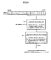
  • the logarithmic transformation lower bit string generating unit 4 comprises a lower bit selecting unit 4a and a lower bit string extracting unit 4b.
  • logarithmic transformation upper bit string generating unit 3 and the logarithmic transformation lower bit string generating unit 4 may be formed independently of each other, whereas they may be integrated into one or more circuits.
  • these components 3, 4, 3a, 3b, 4a, and 4b need not necessarily be configured independently. Instead, they may be integrated into one or more circuits to shrink the circuit scale by sharing logic operation elements, some of the circuitry, etc.
  • a logarithmic transformation upper bit string generating unit 3 when the logarithmic transformation upper bit string generating unit 3 is supplied with n-bit input data B to be transformed, it detects a highest order bit of logic "1" (hereinafter, referred to as "active bit") out of the bits b n-1 , b n-2 , b n-3 , ..., b 2 , b 1 , and b 0 of the input data B.
  • active bit a highest order bit of logic "1"
  • This detecting process is performed by the active bit detecting unit 3a in Fig. 3, whereby the foregoing highest order bit is detected as the active bit. Then, the bit number S for indicating what number of the bit of the input data B the active bit falls on is identified.
  • the bit number S of the bit b n-k is n - k.
  • bits of logic "1" among the bits b 11 -b 0 of order lower than the bit b 12 , if any, are not regarded as active bits.
  • the active bit detecting unit 3a supplies the bit number S to the upper bit string generating unit 3b and the logarithmic transformation lower bit string generating unit 4 as the result of detection of the active bit.
  • the upper bit string generating unit 3b generates a logarithmic transformation upper bit string D UP (d m-1, d m-2 , d m-3 , ..., d m-p ) , or the upper p bits including the most significant bit d m-1, of the m-bit logarithmic transformation data D.
  • bit number S is supplied from the active bit detecting unit 3a
  • binary data equivalent to the bit number S (binary data consisting of p bits) is generated.
  • the p-bit binary data makes the logarithmic transformation upper bit string D UP .
  • the bit number S of the active bit is "12." Then, binary data (1, 1, 0, 0) equivalent to the bit number S is generated.
  • the logarithmic transformation upper bit string generating unit 3 including the active bit detecting unit 3a and the upper bit string generating unit 3b generates the bit number S of the active bit in the form of the logarithmic transformation upper bit string D UP , with the highest order bit as the active bit out of the bits of the input data B which have logic "1.”
  • the logarithmic transformation lower bit string generating unit 4 When the logarithmic transformation lower bit string generating unit 4 is supplied with n-bit input data B to be transformed, it generates a logarithmic transformation lower bit string D LOW , which represents the lower (m - p) bits of the logarithmic transformation data D, based on the input data B.
  • the lower bit selecting unit 4a selects a bit string (b n-k-1, b n-k-2 , ..., b 1 , b 0 ) of order lower than the active bit b n-k designated by the foregoing bit number S, out of the bits b n-1 , b n-2, b n-3, ..., b 2 , b 1 , and b 0 of the input data B, and outputs the result of selection to the lower bit string extracting unit 4b.
  • the lower bit string (b n-k-1 , b n-k-2, ..., b 1 , b 0 ) is selected based on the bit number S, whereas other methods are also applicable.
  • the lower bit string (b n-k-1 , b n-k-2, ..., b 1 , b 0 ) may be selected based on the p-bit logarithmic transformation upper bit string D UP (d m-1 , d m-2 , ..., d m-p ) described above.
  • the logarithmic transformation upper bit string D UP (d m-1 , d m-2 , ..., d m-p ) is the binary data of the bit number S
  • the lower bit string (b n-k-1, b n-k-2 , ..., b 1 , b 0 ) may be selected based on the logarithmic transformation upper bit string D UP (d m-1, d m-2 , ..., d m-p ) instead of the bit number S.
  • the lower bit string extracting unit 4b extracts upper q bits from the lower bit string (b n-k-1 , b n-k-2, ..., b 1, b 0 ) , the number of bits q corresponding to a difference (m - p) between the number of bits m of the logarithmic transformation data D to be generated and the number of bits p of the logarithmic transformation upper bit string D UP.
  • the extracted string of q (i.e., m - p) bits (b n-k-1, b n-k-2, ..., b n-k-1-q ) makes the logarithmic transformation lower bit string D LOW (d m-p-1, d m-p-2 , ..., d 1 , d 0 ) of the logarithmic transformation data D.
  • the p-bit logarithmic transformation upper bit string D UP (d m-1 , d m-2, d m-3, ..., d m-p ) is output as an integral value resulting from the logarithmic transformation of the input data B.
  • the q-bit logarithmic transformation lower bit string D LOW (d m-p-1 , ..., d 2 , d 1 , d 0 ) is output as a fractional value resulting from the logarithmic transformation of the input data B.
  • the logarithmic transformation data D having a total of m bits is output with the logarithmic transformation upper bit string D UP and the logarithmic transformation lower bit string D LOW as the upper bit string and the lower bit string of the logarithmic transformation data D, respectively.
  • the lower bit string extracting unit 4b performs the following processing.
  • the logarithmic transformation upper bit string D UP (d m-1 , d m-2 , ..., d m-p ) is D UP (1, 1, 0, 0) as described above since the highest order bit of logic "1" falls on the twelfth bit b 12 .
  • the remaining four bits (m - p 4) are allocated for the logarithmic transformation lower bit string D LOW .
  • bit string D LOW As a candidate for the logarithmic transformation lower bit string D LOW , the bit string (0, 1, 1, 0, 1, 0, 0, 0, 0, 0, 1), or the bit string (b 11 , b 10 , b 9 , b 8 , ..., b 0 ) of order lower than the foregoing twelfth bit b 12 , is selected from the input data B (0, 0, 0, 1, 0, 1, 1, 0, 1, 0, 0, 0, 0, 0, 1).
  • bit string (0, 1, 1, 0) corresponding to the string of upper four bits makes the logarithmic transformation lower bit string D LOW (d 3 , d 2 , d 1 , d 0 ), i.e., D LOW (0, 1, 1, 0).
  • the logarithmic transformation upper bit string D UP (1, 1, 0, 0) and the logarithmic transformation lower bit string D LOW (0, 1, 1, 0) are combined into the final logarithmic transformation data D (1, 1, 0, 0, 0, 1, 1, 0).
  • a pointer t attached to the logarithmic transformation data D given the transformation indicates the position of the decimal point. Consequently, in such cases that the logarithmic transformation data D is buffered by a register circuit or the like for parallel output, the physical bit position in the register circuit or the like can be represented by the pointer t to indicate the boundary (the position of the decimal point) between the logarithmic transformation upper bit string D UP and the logarithmic transformation lower bit string D LOW .
  • the mode of expression of the boundary (the point of the decimal point) between the logarithmic transformation upper bit string D UP and the logarithmic transformation lower bit string D LOW of the logarithmic transformation data D is not limited to the pointer t.
  • a single bit may be added to the position of the boundary between the logarithmic transformation upper bit string D UP and the logarithmic transformation lower bit string D LOW .
  • the logarithmic transformation data D has a total of (m + 1) bits with the single additional bit as a bit indicating the position of the decimal point.
  • a single bit may be added to the position of the boundary between the logarithmic transformation upper bit string D UP and the logarithmic transformation lower bit string D LOW while the least significant bit d 0 of the logarithmic transformation lower bit string D LOW is removed.
  • the logarithmic transformation data D has a total of m bits with the single additional bit as a bit indicating the position of the decimal point.
  • the logarithmic transformation of input data B resulted in logarithmic transformation data D showing values in close agreement with its theoretical values.
  • the accuracy of the logarithmic transformation will be described specifically in conjunction with the following practical example.
  • the logarithmic transformation data D showed values in close agreement with the theoretical values.
  • the logarithmic transformer of the present embodiment can be made of logic operation elements extremely fewer than with the conventional address decoder 1 shown in Fig. 1. This allows a reduction in circuit scale etc.
  • the logarithmic transformation upper bit string generating unit 3 can detect and identify the active bit and the bit number S in the input data B by using a small-scale comparator or decoder circuit which is composed of logic operation elements.
  • the binary data can be generated from the bit number S by using a small-scale decoder circuit which is composed of logic operation elements.
  • the logarithmic transformation lower bit string generating unit 4 can be implemented as a small-scale register circuit or the like since it determines the logarithmic transformation lower bit string D LOW by simply selecting and extracting predetermined bits from the input data B.
  • the circuit scale can also be reduced due to the absence of the configuration where data corresponding to logarithmic transformation is prestored in a ROM or the like as if in the prior art.
  • the logarithmic transformer of the present embodiment has a new configuration which allows a reduction in circuit scale and the like with useful effects in the field of digital signal processing.
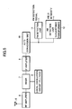
  • Fig. 5 is a diagram showing the configuration of an FM/AM receiver which utilizes the logarithmic transformer of this practical example.
  • Figs. 6 and 7 are diagrams showing the circuitry of the logarithmic transformer.
  • Figs. 8 to 11 are charts showing the operation and function of the logarithmic transformer.
  • Fig. 12 is a chart showing evaluation of the logarithmic transformer.
  • the FM/AM receiver utilizing the logarithmic transformer of this practical example comprises an RF amplifier 6, a mixer 7, a local oscillation circuit 8, and an IF amplifier 9.
  • the RF amplifier 6 receives arrival waves through an antenna 5.
  • the local oscillation circuit 8 has such circuits as a PLL and a VCO, and generates a local oscillation signal.
  • the mixer 7 mixes the local oscillation signal and the reception signal to generate an intermediate frequency signal (IF signal) and the like.
  • the IF amplifier 9 amplifies the intermediate frequency signal.
  • the FM/AM receiver further comprises an A/D conversion unit 10, an FM detection unit 11, and an AM detection unit 12.
  • the A/D conversion unit 10 performs analog-to-digital conversion to convert the intermediate frequency signal amplified by the IF amplifier 9 into digital data.
  • the FM detection unit 11 applies predetermined digital signal processing to the digital data to detect an FM detection signal.
  • the AM detection unit 12 applies predetermined digital signal processing to the digital data to detect an AM detection signal.
  • the AM detection unit 12 not only generates the foregoing AM detection signal but also performs full-wave rectification on the digital data supplied from the A/D conversion unit 10 for AM detection.
  • the AM detection unit 12 thus outputs data which indicates field intensity for use in detecting the presence or absence of sending stations or the like.
  • the data indicating field intensity generated through the full-wave rectification and AM detection, is linear data.
  • the linear data is hard to process as-is.
  • the logarithmic transformer of this practical example is provided to logarithmically transform the data indicating field intensity before processing.
  • the circuits shown in Fig. 6 constitute the logarithmic transformation upper bit string generating unit 3 shown in Fig. 2.
  • the circuits shown in Fig. 7 constitute the logarithmic transformation lower bit string generating unit 4 shown in Fig. 2.
  • the logarithmic transformation upper bit string generating unit 3 comprises 15 OR gates U 14 -U 0 , 15 AND gates G 14 -G 0 , and a multiplexer 13.
  • the multiplexer 13 has a data input port consisting of 17 input terminals which are designated by the symbols d in the diagram, and a switching control port consisting of 17 control terminals which are designated by the symbols e in the diagram.
  • the multiplexer 13 also comprises an output port for parallel-outputting 3-bit binary data which is designated by the symbols d 6 , d 5 , and d 4 in the diagram.
  • the input terminals d of the data input port are respectively given 3-bit binary data (0, 0, 0) to (1, 1, 1) corresponding to decimal values of "0" to "7" in advance.
  • the input terminal d lying at the top in the diagram (the counterpart of the control terminal e to which a decode bit g 15 to be described later is applied) is given binary data (1, 1, 1).
  • the next input terminal d is given binary data (1, 1, 0), and the next input terminal d binary data (1, 0, 1).
  • the rest of the input terminals d are also previously given predetermined binary data out of the 3-bit binary data (0, 0, 0) to (1, 1, 1).
  • resistors to a so-called power supply terminal and ground terminal.
  • control terminals e are individually supplied with decode bits g 15 -g 0 and h 0 to be described later, respectively.
  • a single input terminal d and a single control terminal e shown adjoining each other constitute each single pair.
  • the above-mentioned binary data applied to the input terminal d which is paired with the control terminal e is output from the output port as output data (d 6 , d 5 , d 4 ).
  • the multiplexer 13 performs multiplexing so that the binary data applied to the input terminal d paired with the control terminal e of logic "1" makes the output data (d 6 , d 5 , d 4 ).
  • the OR gates U 14 -U 0 and the AND gates G 14 -G 0 are wired in predetermined combinations to decode the 16-bit input data B (b 15 , b 14 , ..., b 1 , b 0 ), or the most significant bit (MSB) b 15 to the least significant bit (LSB) b 0 , into 16-bit decode data G (g 15 , g 14 , ..., g 1 , g 0 ) and decode the single decode bit h 0 .
  • the resultant is output to the foregoing 17 control terminals e in parallel.
  • the most significant decode bit g 15 of the decode data G is not associated with any of the foregoing OR gates and AND gates.
  • the most significant bit b 15 of the input data B is then supplied as-is to the highest-order control terminal e of the multiplexer 13.
  • the AND gates G 14 -G 0 are of two input type, each having an input terminal of inverted logic and the other input terminal of non-inverted logic.
  • the OR gates U 14 -U 0 are of two input type each.
  • the OR gates U 14 -U 0 and the AND gates G 14 -G 0 are arranged in accordance with the respective bits b 15, b 14 , ..., b 1, and b 0 of the input data B.
  • the OR gates U 14 -U 0 are cascaded from the higher order to the lower, so as to perform OR operations between the outputs of the respective OR gates of higher order and predetermined bits of the input data B (b 15 , b 14 , ..., b 1 , b 0 ) .
  • the outputs u 14 -u 1 of the OR gates U 14- U 1 are supplied to the logic-inverted input terminals of the AND gates G 13 -G 0 , respectively.
  • the decode bits g 14 -g 0 to be output from the AND gates G 14 -G 0 are wired to predetermined control terminals e of the multiplexer 13.
  • OR gates U 14 -U 0 operate so that the OR gate corresponding to a highest order bit of logic "1," out of the bits b 15 -b 0 of the input data B, and the OR gates of order lower than the OR gate all output logic "1.”
  • the OR gates U 14 -U 0 detect a highest order bit of logic "1" out of the bits b 15 -b 0 of the input data B and set all the outputs of the OR gates corresponding to the bit of logic "1" and lying below the bit to logic "1,” thereby outputting the aforementioned candidate for the active bit.
  • the AND gate G 14 performs an AND operation between the bits b 15 and b 14 .
  • the AND gates G 13 -G 0 perform AND operations between the outputs u 14 -u 1 from the OR gates U 14 -U 1 and the bits b 13 -b 0 , respectively. Then, the result of detection indicating the true active bit (that is, a single active bit) and its bit number S is output based on the decode bit g 15 and the outputs (decode bits) g 14 -g 0 of these AND gates G 14 -G 0 .
  • the output u 14 of the OR gate U 14 becomes logic “1” due to the logic "1" of the bit b 15 .
  • the outputs u 13 -u 1 of the remaining OR gates U 13 -U 1 also become logic “1.”
  • the outputs u 14 -u 1 each having logic “1” are applied to the logic-inverted input terminals of the AND gates G 13 -G 0 .
  • the AND gates G 13 -G 0 output the decode bits g 13 -g 0 of logic "0" each.
  • the fourteenth bit b 14 of the input data B is the highest order bit of logic "1," only the bit g 14 out of the decode bits g 15 -g 0 becomes logic "1." With the fourteenth bit b 14 as the true active bit, the bit number S (i.e., 14) is then detected and identified.
  • the bit number S (i.e., 13) is then detected and identified.
  • the multiplexer 13 outputs the binary data of an input terminal d which corresponds to the control terminal e to which logic "1" is applied, out of the 17 control terminals e, as a bit string (d 6 , d 5 , d 4 ) from its output port.
  • bit string (d 6 , d 5 , d 4 ) output corresponds to the active bit of the input data B.
  • the input terminals d are given binary data corresponding to respective bit numbers S in advance.
  • the binary data equivalent to the bit number S of the active bit represented by the decode bits g 15 -g 0 is thus output as the bit string (d 6 , d 5 , d 4 ) .
  • bit string (b 15 -b 7 ) or the fifteenth to seventh bits of the input data B, contains any bit of logic "1," the output u 8 of the OR gate U 8 always becomes logic "1.”
  • the bit d 7 of the logarithmic transformation upper bit string D UP (d 7 , d 6, d 5 , d 4 ) then becomes logic "1.”
  • bit d 7 of the logarithmic transformation upper bit string D UP (d 7 , d 6 , d 5 , d 4 ) is set at either logic “1” or “0” depending on whether any one of the bits of the bit string (b 15 -b 7 ), or the fifteenth to seventh bits of the input data B, is of logic "1” or all the bits are of logic “0.” This allows the generation of the logarithmic transformation upper bit string D UP equivalent to the bit number S of the active bit.
  • Figs. 8 and 9 are charts showing the above-described operation of the logarithmic transformation upper bit string generating unit 3 in the form of truth tables. Due to space limitation, the shown outputs of the logarithmic transformation upper bit string D UP are for typical values of the input data B. The input data B is shown both in decimal and in binary. The values of the logarithmic transformation upper bit string D UP are in decimal.
  • logarithmic transformation upper bit strings D UP when various values of the input data B are input, logarithmic transformation upper bit strings D UP are output, the strings Dup being equivalent to the bit numbers S of respective highest order bits of logic "1" (active bits) in the bits of the input data B.
  • the output values of the logarithmic transformation upper bit strings D UP in decimal expression thus indicate the integral values of the respective logarithmic transformations of the input data B.
  • bit numbers S of the active bits shown boxed are logarithmically transformed with the bits of order lower than the active bits (represented by the symbol "*") as don't-care.
  • the integral parts of the resultant logarithms are output as the logarithmic transformation upper bit strings D UP .
  • This logarithmic transformation lower bit string generating unit 4 comprises a plurality of AND gates X 15 -X 1 , an OR gate X 0 , and a multiplexer 14.
  • the multiplexer 14 has a configuration similar to that of the multiplexer 13 shown in Fig. 13, having a data input port consisting of 16 input terminals d and a switching control port consisting of 16 control terminals e to be paired with the respective input terminals d.
  • the 4-bit binary data applied to the input terminal d to be paired with the control terminal is output as the logarithmic transformation lower bit string D LOW (d 3 , d 2 , d 1 , d 0 ) .
  • the highest-order control terminal e of the multiplexer 14 and the output of the AND gate X 15 are connected to each other.
  • the next control terminal e and the output of the AND gate X 14 are connected to each other.
  • the next control terminal e and the output of the AND gate X 13 are connected to each other.
  • the rest of the control terminals e and the outputs of the AND gates X 12 -X 1 are successively connected to each other in one-on-one correspondence.
  • the lowest-order control terminal e is connected with the output of the OR gate X 0 .
  • the input terminals d arranged in association with the foregoing 16 control terminals e from the highest order to the lowest, respectively, are supplied with the bits b 14 , b 13 , ..., b 1 , b 0 of the input data B (b 15 , b 14 , ..., b 1 , b 0 ), each with four bits shiftingly assigned.
  • the highest input terminal d paired with the control terminal e which is connected to the AND gate X 15 receives a bit string (b 14 , b 13 , b 12 , b 11 ) in parallel.
  • the input terminal d paired with the control terminal e which is connected to the AND gate X 14 receives a bit string (b 13 , b 12 , b 11, b 10 ) in parallel.
  • the input terminal d paired with the control terminal e which is connected to the AND gate X 13 receives a bit string (b 12 , b 11 , b 10 , b 9 ) in parallel.
  • the rest of the input terminals d successively receive specific four bits of the input data B in parallel.
  • the lowest-order input terminal d (input terminal paired with the control terminal e which is connected to the OR gate X 0 ) of the multiplexer 14 is given binary data (0, 0, 0, 0).
  • the next higher input terminal d is given binary data (b 0 , 0, 0, 0).
  • the next higher two input terminals d are given binary data (b 1 , b 0 , 0, 0) and (b 2 , b 1 , b 0 , 0), respectively.
  • the additional bits of logic "0" are set by means of a simple circuit configuration of connecting pull-down resistors to a so-called ground terminal.
  • the AND gates X 15 -X 1 are of four input type, and are wired to input the logarithmic transformation upper bit string D UP (d 7 , d 6 , d 5 , d 4 ) .
  • predetermined input terminals out of the respective four input terminals of the AND gates X 15 -X 1 are of inverted logic.
  • the AND gates X 15 -X 1 thus detect the binary value of the logarithmic transformation upper bit string D UP (d 7 , d 6 , d 5 , d 4 ) , thereby detecting the bit number S of the active bit described above.
  • the twelfth bit b 12 corresponding to the logarithmic transformation upper bit string Dup (1, 1, 0, 0) is detected as the active bit.
  • the output of the AND gate X 12 having logic "1," is supplied to the predetermined control terminal e of the multiplexer 14.
  • the input terminal d corresponding to the control terminal e which is connected to the AND gate X 12 is given the binary data of the bit string (b 11 -b 8 ), or the eleventh to eighth bits of the input data B.
  • a bit string (0, 1, 1, 0) out of the foregoing input data B (0, 0, 0, 1, 0, 1, 1, 0, 1, 0, 0, 0, 0, 0, 1) is thus output from the multiplexer 14 as the logarithmic transformation lower bit string D LOW (d 3 , d 2 , d 1 , d 0 ).
  • the AND gates X 15 -X 1 detect the bit number S of the active bit represented by the logarithmic transformation upper bit string D UP (d 7 , d 6 , d 5 , d 4 ) , and make the multiplexer 14 output the data of the string of four bits lower than the bit number S out of the bit string of the input data B.
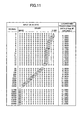
  • Figs. 10 and 11 are charts showing the operation in the form of truth tables.
  • the input data B is shown in decimal and in binary.
  • the values of the logarithmic transformation data D generated finally are shown in decimal.
  • the logarithmic transformation upper bit string generating unit 3 generates a logarithmic transformation upper bit string D UP based on the active bit, shown boxed in the diagram, out of the bits of the input data B.
  • the logarithmic transformation lower bit string generating unit 4 transforms four bits of order lower than the active bit, out of those indicated by the symbol "*" in Fig. 9, into a logarithmic transformation lower bit string D LOW which shows the value of the fractional part.
  • logarithmic transformation data D is generated with the logarithmic transformation upper bit string D UP and the logarithmic transformation lower bit string D LOW , which express the integral part of the logarithmic transformation value and the fractional part of the logarithmic transformation value, respectively, with the symbol " ⁇ " as the boundary therebetween.
  • the logarithmic transformation lower bit string generating unit 4 uses the circuits shown in Fig. 7 to perform the processing of selecting and extracting the logarithmic transformation lower bit string D LOW , which expresses the fractional part of the logarithmic transformation value, from the input data B.
  • the logarithmic transformation lower bit string D LOW is output as the bit string of lower order to follow the logarithmic transformation upper bit string D UP .
  • the logarithmic transformation upper bit string D UP generated based on a boxed active bit is followed by the logarithmic transformation lower bit string D LOW which is the output of an intact string of four bits of order lower than the active bit.
  • this logarithmic transformer outputs the m-bit binary data composed of the logarithmic transformation upper bit string D UP and the logarithmic transformation lower bit string D LOW as the logarithmic transformation data D.
  • the logarithmic transformation data D shows the result of logarithmic transformation in the form of the sum of an integral value and a fractional value as shown in decimal in Fig. 11. Since the fractional value is added to the integral value of insufficient accuracy, it is possible to generate logarithmic transformation data D of higher accuracy.
  • Fig. 12 is a chart for showing the accuracy of transformation of the logarithmic transformer in this practical example. The shown evaluation is for the case where 16-bit input data B is logarithmically transformed into 8-bit logarithmic transformation data D.
  • logarithmic transformation can be performed by fewer logic operation elements. It is therefore possible to achieve a significant reduction in circuit scale and the like. The processing time necessary for the logarithmic transformation can also be reduced greatly. Besides, high logarithmic transformation accuracy can be obtained as shown in Fig. 12.
  • the binary data string (logarithmic transformation lower bit string) D LOW for expressing the fractional part of a logarithmic transformation value is extracted from a bit string of order lower than the active bit in the input data B.
  • the resultant is then combined with the logarithmic transformation upper bit string D UP to finally generate the logarithmic transformation data D.
  • the processing of extraction from a bit string of order lower than the active bit in the input data B is performed only once before the resultant is simply combined with the logarithmic transformation upper bit string D UP to generate the logarithmic transformation data D. This allows a significant reduction in the time necessary for the logarithmic transformation processing.
  • the logarithmic transformation lower bit string D Low which expresses the fractional part of the logarithm is generated from the binary data corresponding to the position of the fractional active bit (binary data expressing the fractional value) and the remaining bit string of order lower than the fractional active bit.
  • logarithmic transformation data D which precisely expresses the fractional part of the logarithm even if the number of bits of the binary data for expressing the fractional part of the logarithm needs to be reduced in order to satisfy general requirements in generating logarithmic transformation data D in a limited number of bits m. In other words, it is possible to improve the resolution of the fractional logarithm with a smaller number of bits. This in turn allows the generation of logarithmic transformation data D corresponding to input data B with high accuracy.
  • processing of detecting a fractional active bit may be repeated a plurality of times (two or more times) .
  • the double or multiple processing can further improve the resolution of the fractional logarithm, allowing logarithmic transmission data Dm of higher accuracy.
  • the embodiment and the practical example have dealt mainly with a logarithmic transformer which is configured as hardware.
  • the logarithmic transformer may be a computer program for logarithmic transformation which is run on an electronic apparatus comprising a computer (CPU) or the like capable of digital processing.
  • a computer program having the function equivalent to that of the logarithmic transformer described in the embodiment and the practical example can be created and run on an electronic apparatus such as a personal computer (PC), to achieve a significant reduction in the processing time required for logarithmic transformation with high logarithmic transformation accuracy etc.
  • PC personal computer

Landscapes

  • Physics & Mathematics (AREA)
  • General Physics & Mathematics (AREA)
  • Engineering & Computer Science (AREA)
  • Computational Mathematics (AREA)
  • Mathematical Analysis (AREA)
  • Pure & Applied Mathematics (AREA)
  • Theoretical Computer Science (AREA)
  • Computing Systems (AREA)
  • Mathematical Optimization (AREA)
  • General Engineering & Computer Science (AREA)
  • Compression, Expansion, Code Conversion, And Decoders (AREA)

Abstract

A logarithmic transformer capable of a reduction in circuit scale. A logarithmic transformation upper bit string generating unit (3) detects a highest order bit of logic "1" out of the bits bn-1, ..., b0 of input data B as an active bit. Binary data for indicating the bit position S of the active bit is generated as a logarithmic transformation upper bit string DUP (dm-1, ..., dm-p). Here, based on the number of bits n of the input data B, the number of bits p of the logarithmic transformation upper bit string DUP (dm-1, ..., dm-p) is set for the relationship n = 2P. A logarithmic transformation lower bit string generating unit (4) determines a bit string of order lower than the bit position S, having a predetermined number q of bits, out of the bits bn-1, ..., b0 of the input data B. The resultant bit string makes a logarithmic transformation lower bit string DLOW (dm-p-1, ..., d0). Then, logarithmic transformation data D having a total number of p + q bits is generated with the logarithmic transformation upper bit string DUP (dm-1, ..., dm-p) as the integral part of a logarithmic transformation value resulting from the logarithmic transformation of the input data B and the logarithmic transformation lower bit string DLOW (dm-p-1, ..., d0) as the fractional part of the logarithmic transformation value resulting from the logarithmic transformation of the input data B.

Description

    BACKGROUND OF THE INVENTION
  • The invention relates to a logarithmic transformer and a method of logarithmic transformation for logarithmically transforming, for example, digital data or the like.
  • Conventionally, in compressing a large number of bits of digital data into fewer bits of digital data and in improving operation efficiency by replacing a multiplication or division between a plurality of pieces of digital data with an addition or subtraction between pieces of digital data which are logarithmically transformed, logarithmic transformation has widely been used as useful means in the field of digital signal processing.
  • Fig. 1A shows the configuration of a typical logarithmic transformer which has been known heretofore.
  • This logarithmic transformer is implemented as hardware for the sake of fast logarithmic transformation. As shown in Fig. 1A, the logarithmic transformer includes an address decoder 1 which is a logic circuit and a logarithmic ROM 2 which is made of a read-only semiconductor memory.
  • The logarithmic ROM 2 is configured as a so-called look-up table, in which a number of pieces of logarithmic transformation data corresponding to digital data to be logarithmically transformed are stored in advance.
  • When the address decoder 1 receives digital data to be logarithmically transformed, it transforms (decodes) the digital data into address data to designate an address of the logarithmic ROM 2 so that logarithmic transformation data corresponding to the digital data is read out.
  • That is, the values of digital data to be logarithmically transformed, the address data for designating addresses of the logarithmic ROM 2, and the logarithmic transformation data prestored at the addresses designated by the address data are determined in one-on-one correspondence. Thus, when digital data to be logarithmically transformed is supplied to the address decoder 1, the logarithmic transformation data corresponding to the digital data is output from the logarithmic ROM 2 as a result of logarithmic transformation, thereby allowing fast logarithmic transformation.
  • The conventional logarithmic transformer, however, has had a problem of being extremely large in circuit scale.
  • This has been a significant problem to be solved in such cases that the logarithmic transformer is incorporated into an electronic apparatus requiring high density packaging, reduced size and weight, etc., and that the logarithmic transformer is formed as a semiconductor integrated circuit device.
  • Take a concrete example. The address decoder 1 shown in Fig. 1A is composed of a plurality of stages of logic circuits 1a and 16 as shown in Fig. 1B. Each of the logic circuits 1a and 1b includes a number of logic operation elements (inverters, OR gates, NOR gates, AND gates, NAND gates, etc.) in combination.
  • Here, the plurality of logic circuits 1a lying in the first stage are made of a plurality of inverters and NOR gates for creating intricate combinations of n-bit (n is an arbitrary natural number) input digital data for logic operation. The logic circuit 1b in the next stage is also made of a plurality of logic operation elements so that a number of pieces of data output from the plurality of logic circuits 1a are intricately combined for logic operation. The logic circuit 1b includes a number of stages of logic circuits, not a single stage alone.
  • As above, due to such reasons as the necessity to generate address data capable of accessing the entire address space of the logarithmic ROM 2, the address decoder 1 has had a large circuit scale.
  • The look-up table configuration of the logarithmic ROM 2 has also contributed an increase in circuit scale.
  • That is, the logarithmic ROM 2 must previously contain at least 2n values of logarithmic transformation data according to the number of bits n of the digital data to be logarithmically transformed.
  • In addition, even if the logarithmic transformation data is stored as m bits of data which is smaller than the n-bit digital data, the logarithmic ROM 2 still requires a total memory capacity of at least 2n × m bits.
  • Under the circumstances, the logarithmic ROM 2 has required a high memory capacity, contributing to the large circuit scale.
  • SUMMARY OF THE INVENTION
  • The present invention has been achieved in view of the conventional problems illustrated above. It is thus an object of the present invention to provide a logarithmic transformer having a new configuration.
  • According to a first aspect of the present invention, there is provided a logarithmic transformer comprising: a first bit string generator for generating a first bit string of binary data indicating the position of a highest order bit of logic "1" out of bits of digital data to be logarithmically transformed; and a second bit string generator for determining, from the digital data, a second bit string of order lower than the highest order bit of logic "1", the logarithmic transformer outputting logarithmic transformation data, which includes the first bit string as an integral part of a logarithmic transformation value resulting from a logarithmic transformation of the digital data and the second bit string as a fractional part of the logarithmic transformation value.
  • According to a second aspect of the present invention, the first bit string generator comprises: a detecting unit for detecting the position of the highest order bit of logic "1" out of the bits of the digital data; and a generating unit for generating the first bit string based on a result of detection by the detecting unit.
  • According to a third aspect of the present invention, the detecting unit detects the highest order bit of logic "1" by decoding the digital data.
  • According to a fourth aspect of the present invention, the generating unit contains pieces of binary data indicating the positions of the respective bits of the digital data, and selects one out of the pieces of binary data based on the result of detection by the detecting unit, thereby generating the binary data indicating the position of the highest order bit of logic "1."
  • According to a fifth aspect of the present invention, the generating unit is composed of a switching circuit for selecting one out of the pieces of binary data, based on the result of detection by the detecting unit.
  • According to a sixth aspect of the present invention, the detecting unit comprises: a first logic circuit for outputting data for excluding a bit string lower than the highest order bit of logic "1" from the bits of the digital data; and a second logic circuit for removing the bit string excluded by the data from the bits of the digital data, thereby detecting the highest order bit of logic "1."
  • According to a seventh aspect of the present invention, the first logic circuit includes a plurality of OR gates for inputting respective bits of the digital data from a most significant bit to a least significant bit, the OR gates having their outputs and inputs cascaded in association with the most significant bit to the least significant bit; and the OR gates generate the data for excluding by performing OR operations between the outputs of the OR gates of higher order bits and the respective bits of the digital data.
  • According to an eighth aspect of the present invention, the second logic circuit detects the highest order bit of logic "1" by performing AND operations between the respective bits of the digital data and the data for excluding.
  • According to a ninth aspect of the present invention, the second bit string generator determines, as the second bit string, a bit string of a predetermined number of bits including a bit following the highest order bit of logic "1" out of the bits of the digital data.
  • According to a tenth aspect of the present invention, when the number of bits from the bit following the highest order bit to a least significant bit of the digital data falls short of the predetermined number, the second bit string generator appends as many bits as a shortfall to the least significant bit to generate, as the second bit string, a bit string of the predetermined number of bits.
  • According to an eleventh aspect of the present invention, the secondbit string generator comprises: a second bit string extracting unit for inputting the digital data as successive bit strings each having the predetermined number of bits; and a second bit string selecting unit for making the second bit string extracting unit to extract, as the second bit string, a bit string of the predetermined number of bits having the bit following the highest order bit of logic "1" as a most significant bit of the bit string of the predetermined number.
  • According to a twelfth aspect of the present invention, the second bit string selecting unit detects the highest order bit of logic "1" by decoding the digital data.
  • According to a thirteenth aspect of the present invention, the second bit string extracting unit extracts the bit string of the predetermined number of bits including the bit following the highest order bit as the most significant bit, based on the result of detection decoded by the second bit string selecting unit.
  • According to a fourteenth aspect of the present invention, the second bit string extracting unit is composed of a switching circuit for extracting the bit string of the predetermined number of bits based on the result of detection by the second bit string selecting unit.
  • According to a fifteenth aspect of the present invention, there is provided a logarithmic transformation comprising: a first bit string generating step of generating a first bit string of binary data indicating the position of a highest order bit of logic "1" out of bits of digital data to be logarithmically transformed; and a second bit string generating step of determining, from the digital data, a second bit string of order lower than the highest order bit of logic "1". Specifically, logarithmic transformation data on the digital data is generated by using the first bit string as an integral part of a logarithmic transformation value resulting from a logarithmic transformation of the digital data and the second bit string as a fractional part of the logarithmic transformation value.
  • RIEF DESCRIPTION OF THE DRAWINGS
  • These and other objects and advantages of the present invention will become clear from the following description with reference to the accompanying drawings, wherein:
  • Figs. 1A and 1B are diagrams showing the configuration of a conventional logarithmic transformer;
  • Fig. 2 is a diagram explaining the configuration and operation of a logarithmic transformer according to an embodiment of the present invention;
  • Fig. 3 is a diagram further explaining the configuration and operation of the logarithmic transformer according to the embodiment of the present invention;
  • Fig. 4 is a diagram further explaining the configuration and operation of the logarithmic transformer according to the embodiment of the present invention;
  • Fig. 5 is a diagram showing the configuration of an electronic apparatus to which the logarithmic transformer of a practical example is applied;
  • Fig. 6 is a diagram showing the configuration of circuits provided in the logarithmic transformer of this practical example;
  • Fig. 7 is a diagram further showing the configuration of circuits provided in the logarithmic transformer of this practical example;
  • Fig. 8 is a chart explaining the operation of the logarithmic transformer in this practical example;
  • Fig. 9 is a chart further explaining the operation of the logarithmic transformer in this practical example;
  • Fig. 10 is a chart further explaining the operation of the logarithmic transformer in this practical example;
  • Fig. 11 is a chart further explaining the operation of the logarithmic transformer in this practical example; and
  • Fig. 12 is a chart showing the evaluation on the transformation accuracy of the logarithmic transformer in this practical example.
  • DETAILED DESCRIPTION OF THE PREFERRED EMBODIMENTS
  • Hereinafter, a preferred embodiment of the present invention will be described with reference to Figs. 2-4.
  • Figs . 2 to 4 are diagrams showing the configuration and function of a logarithmic transformer according to the present embodiment.
  • For ease of explanation, digital data B to be logarithmically transformed will be described as n-bit binary data which is generally expressed such as B (bn-1, bn-2, bn-3, ..., b2, b1, b0) . Similarly, logarithmic transformation data D given a logarithmic transformation shall be m-bit binary data which can be expressed such as D (dm-1, dm-2, dm-3, ..., dm-p, dm-p-1, ..., d2, d1, d0) .
  • In consideration of the meaning of typical logarithmic transformations, the numbers of bits n and m of the foregoing data B and D will be described, though not necessarily be restrictive, as n ≥ m.
  • In Fig. 2, this logarithmic transformer applies the processing of logarithmic transformation to the input data B to be logarithmically transformed, and outputs the logarithmic transformation data D which results from the logarithmic transformation.
  • In order to perform such logarithmic transformation, the logarithmic transformer comprises a logarithmic transformation upper bit string generating unit 3 and a logarithmic transformation lower bit string generating unit 4.
  • As shown in Fig. 3, the logarithmic transformation upper bit string generating unit 3 comprises an active bit detecting unit 3a and an upper bit string generating unit 3b.
  • As shown in Fig. 4, the logarithmic transformation lower bit string generating unit 4 comprises a lower bit selecting unit 4a and a lower bit string extracting unit 4b.
  • Note that the logarithmic transformation upper bit string generating unit 3 and the logarithmic transformation lower bit string generating unit 4, as well as the active bit detecting unit 3a, the upper bit string generating unit 3b, the lower bit selecting unit 4a, and the lower bit string extracting unit 4b, may be formed independently of each other, whereas they may be integrated into one or more circuits.
  • That is, for the sake of optimum logic design, these components 3, 4, 3a, 3b, 4a, and 4b need not necessarily be configured independently. Instead, they may be integrated into one or more circuits to shrink the circuit scale by sharing logic operation elements, some of the circuitry, etc.
  • In Figs. 2 and 3, when the logarithmic transformation upper bit string generating unit 3 is supplied with n-bit input data B to be transformed, it detects a highest order bit of logic "1" (hereinafter, referred to as "active bit") out of the bits bn-1, bn-2, bn-3, ..., b2, b1, and b0 of the input data B.
  • This detecting process is performed by the active bit detecting unit 3a in Fig. 3, whereby the foregoing highest order bit is detected as the active bit. Then, the bit number S for indicating what number of the bit of the input data B the active bit falls on is identified.
  • For example, when the active bit is the bit bn-k which falls on the kth from the most significant bit (MSB), the bit number S of the bit bn-k is n - k.
  • In a more specific example, when the input data B is 16-bit (n = 16) data expressed as B (0, 0, 0, 1, 0, 1, 1, 0, 1, 0, 0, 0, 0, 0, 0, 1), the bit bn-k of logic "1" falling on the fourth from the most significant bit (MSB) b15 (i.e., b12) is the active bit. The bit number S is "12."
  • Note that bits of logic "1" among the bits b11-b0 of order lower than the bit b12, if any, are not regarded as active bits.
  • Then, the active bit detecting unit 3a supplies the bit number S to the upper bit string generating unit 3b and the logarithmic transformation lower bit string generating unit 4 as the result of detection of the active bit.
  • Next, the upper bit string generating unit 3b generates a logarithmic transformation upper bit string DUP (dm-1, dm-2, dm-3, ..., dm-p) , or the upper p bits including the most significant bit dm-1, of the m-bit logarithmic transformation data D.
  • Here, the number of bits p of the logarithmic transformation upper bit string DUP is predetermined in accordance with the input data B of n bits, so as to satisfy the relationship n = 2p (in other words, the relationship p = log2 n).
  • Then, when the bit number S is supplied from the active bit detecting unit 3a, binary data equivalent to the bit number S (binary data consisting of p bits) is generated. The p-bit binary data makes the logarithmic transformation upper bit string DUP.
  • In a more specific example, when the input data B is the foregoing 16-bit data which is expressed as B (0, 0, 0, 1, 0, 1, 1, 0, 1, 0, 0, 0, 0, 0, 0, 1), the bit number S of the active bit is "12." Then, binary data (1, 1, 0, 0) equivalent to the bit number S is generated.
  • From the relationship n = 2p, the number of bits p of the logarithmic transformation upper bit string DUP corresponding to the 16-bit (n = 16) input data B is "4." Since the binary data equivalent to the foregoing bit number S is (1, 1, 0, 0), the 4-bit logarithmic transformation upper bit string is DUP(1, 1, 0, 0).
  • Even if the number of bits m of the logarithmic transformation data D to be generated is smaller than the number of bits n of the input data B, the number of bits p of the logarithmic transformation upper bit string DUP is determined from the relationship n = 2p. Then, the logarithmic transformation upper bit string DUP corresponding to the binary data equivalent to the bit number S, or the p-bit logarithmic transformation upper bit string DUP, is generated.
  • As above, the logarithmic transformation upper bit string generating unit 3 including the active bit detecting unit 3a and the upper bit string generating unit 3b generates the bit number S of the active bit in the form of the logarithmic transformation upper bit string DUP, with the highest order bit as the active bit out of the bits of the input data B which have logic "1."
  • Next, the logarithmic transformation lower bit string generating unit 4 will be described with reference to Figs. 2 and 4.
  • When the logarithmic transformation lower bit string generating unit 4 is supplied with n-bit input data B to be transformed, it generates a logarithmic transformation lower bit string DLOW, which represents the lower (m - p) bits of the logarithmic transformation data D, based on the input data B.
  • In order to generate this logarithmic transformation lower bit string DLOW, there are provided the lower bit selecting unit 4a and the lower bit string extracting unit 4b in Fig. 4.
  • The lower bit selecting unit 4a selects a bit string (bn-k-1, bn-k-2, ..., b1, b0) of order lower than the active bit bn-k designated by the foregoing bit number S, out of the bits bn-1, bn-2, bn-3, ..., b2, b1, and b0 of the input data B, and outputs the result of selection to the lower bit string extracting unit 4b.
  • In the present embodiment, the lower bit string (bn-k-1, bn-k-2, ..., b1, b0) is selected based on the bit number S, whereas other methods are also applicable.
  • In one modified example, the lower bit string (bn-k-1, bn-k-2, ..., b1, b0) may be selected based on the p-bit logarithmic transformation upper bit string DUP (dm-1, dm-2, ..., dm-p) described above. That is, since the logarithmic transformation upper bit string DUP (dm-1, dm-2, ..., dm-p) is the binary data of the bit number S, the lower bit string (bn-k-1, bn-k-2, ..., b1, b0) may be selected based on the logarithmic transformation upper bit string DUP (dm-1, dm-2, ..., dm-p) instead of the bit number S.
  • Next, the lower bit string extracting unit 4b extracts upper q bits from the lower bit string (bn-k-1, bn-k-2, ..., b1, b0) , the number of bits q corresponding to a difference (m - p) between the number of bits m of the logarithmic transformation data D to be generated and the number of bits p of the logarithmic transformation upper bit string DUP. The extracted string of q (i.e., m - p) bits (bn-k-1, bn-k-2, ..., bn-k-1-q) makes the logarithmic transformation lower bit string DLOW (dm-p-1, dm-p-2, ..., d1, d0) of the logarithmic transformation data D.
  • Incidentally, if the total number of bits of the lower bit string (bn-k-1, bn-k-2, ..., b1, b0) is smaller than q (i.e., m - p), as many bits of logic "0" as the shortfall will be appended to the least significant bit (LSB) b0 so that the logarithmic transformation lower bit string DLOW (dm-p-1, dm-p-2,..., d1, d0) is generated in q bits.
  • Then, as shown in Fig. 2, the p-bit logarithmic transformation upper bit string DUP (dm-1, dm-2, dm-3, ..., dm-p) is output as an integral value resulting from the logarithmic transformation of the input data B. The q-bit logarithmic transformation lower bit string DLOW (dm-p-1, ..., d2, d1, d0) is output as a fractional value resulting from the logarithmic transformation of the input data B.
  • Then, the logarithmic transformation data D having a total of m bits is output with the logarithmic transformation upper bit string DUP and the logarithmic transformation lower bit string DLOW as the upper bit string and the lower bit string of the logarithmic transformation data D, respectively.
  • In a more specific example, the lower bit string extracting unit 4b performs the following processing. This concrete example will deal with the case where this logarithmic transformer is configured to generate 8-bit (m = 8) logarithmic transformation data D from 16-bit (n = 16) input data B, and the input data B is the foregoing 16-bit data expressed as B (0, 0, 0, 1, 0, 1, 1, 0, 1, 0, 0, 0, 0, 0, 0, 1).
  • When the input data B (0, 0, 0, 1, 0, 1, 1, 0, 1, 0, 0, 0, 0, 0, 0, 1) is input, the logarithmic transformation upper bit string DUP (dm-1, dm-2, ..., dm-p) is DUP (1, 1, 0, 0) as described above since the highest order bit of logic "1" falls on the twelfth bit b12.
  • Here, the logarithmic transformation upper bit string DUP (1, 1, 0, 0) occupies four bits (p = 4) of the 8-bit (m = 8) logarithmic transformation data D to be generated. The remaining four bits (m - p = 4) are allocated for the logarithmic transformation lower bit string DLOW.
  • As a candidate for the logarithmic transformation lower bit string DLOW, the bit string (0, 1, 1, 0, 1, 0, 0, 0, 0, 0, 0, 1), or the bit string (b11, b10, b9, b8, ..., b0) of order lower than the foregoing twelfth bit b12, is selected from the input data B (0, 0, 0, 1, 0, 1, 1, 0, 1, 0, 0, 0, 0, 0, 0, 1). Then, the bit string (0, 1, 1, 0) corresponding to the string of upper four bits (b11, b10, b9, b8) makes the logarithmic transformation lower bit string DLOW (d3, d2, d1, d0), i.e., DLOW (0, 1, 1, 0).
  • The logarithmic transformation upper bit string DUP (1, 1, 0, 0) and the logarithmic transformation lower bit string DLOW (0, 1, 1, 0) are combined into the final logarithmic transformation data D (1, 1, 0, 0, 0, 1, 1, 0).
  • In Fig. 2, a pointer t attached to the logarithmic transformation data D given the transformation indicates the position of the decimal point. Consequently, in such cases that the logarithmic transformation data D is buffered by a register circuit or the like for parallel output, the physical bit position in the register circuit or the like can be represented by the pointer t to indicate the boundary (the position of the decimal point) between the logarithmic transformation upper bit string DUP and the logarithmic transformation lower bit string DLOW.
  • Nevertheless, the mode of expression of the boundary (the point of the decimal point) between the logarithmic transformation upper bit string DUP and the logarithmic transformation lower bit string DLOW of the logarithmic transformation data D is not limited to the pointer t.
  • In one modified example, a single bit may be added to the position of the boundary between the logarithmic transformation upper bit string DUP and the logarithmic transformation lower bit string DLOW. Here, the logarithmic transformation data D has a total of (m + 1) bits with the single additional bit as a bit indicating the position of the decimal point.
  • In another modified example, a single bit may be added to the position of the boundary between the logarithmic transformation upper bit string DUP and the logarithmic transformation lower bit string DLOW while the least significant bit d0 of the logarithmic transformation lower bit string DLOW is removed. Here, the logarithmic transformation data D has a total of m bits with the single additional bit as a bit indicating the position of the decimal point.
  • According to the present embodiment, the logarithmic transformation of input data B resulted in logarithmic transformation data D showing values in close agreement with its theoretical values. Incidentally, the accuracy of the logarithmic transformation will be described specifically in conjunction with the following practical example. As shown in the evaluations in Fig. 12, when 16-bit input data B was logarithmically transformed by this logarithmic transformer, the logarithmic transformation data D showed values in close agreement with the theoretical values.
  • Moreover, the logarithmic transformer of the present embodiment can be made of logic operation elements extremely fewer than with the conventional address decoder 1 shown in Fig. 1. This allows a reduction in circuit scale etc.
  • For example, the logarithmic transformation upper bit string generating unit 3 can detect and identify the active bit and the bit number S in the input data B by using a small-scale comparator or decoder circuit which is composed of logic operation elements.
  • In generating the p-bit logarithmic transformation upper bit string Dup equivalent to the bit number S, the binary data can be generated from the bit number S by using a small-scale decoder circuit which is composed of logic operation elements.
  • In addition, the logarithmic transformation lower bit string generating unit 4 can be implemented as a small-scale register circuit or the like since it determines the logarithmic transformation lower bit string DLOW by simply selecting and extracting predetermined bits from the input data B.
  • The circuit scale can also be reduced due to the absence of the configuration where data corresponding to logarithmic transformation is prestored in a ROM or the like as if in the prior art.
  • As illustrated above, the logarithmic transformer of the present embodiment has a new configuration which allows a reduction in circuit scale and the like with useful effects in the field of digital signal processing.
  • [Example]
  • Now, with reference to Figs. 5 to 12, description will be given of a more concrete, practical example of embodiment.
  • Fig. 5 is a diagram showing the configuration of an FM/AM receiver which utilizes the logarithmic transformer of this practical example. Figs. 6 and 7 are diagrams showing the circuitry of the logarithmic transformer. Figs. 8 to 11 are charts showing the operation and function of the logarithmic transformer. Fig. 12 is a chart showing evaluation of the logarithmic transformer.
  • In Fig. 5, the FM/AM receiver utilizing the logarithmic transformer of this practical example comprises an RF amplifier 6, a mixer 7, a local oscillation circuit 8, and an IF amplifier 9. The RF amplifier 6 receives arrival waves through an antenna 5. The local oscillation circuit 8 has such circuits as a PLL and a VCO, and generates a local oscillation signal. The mixer 7 mixes the local oscillation signal and the reception signal to generate an intermediate frequency signal (IF signal) and the like. The IF amplifier 9 amplifies the intermediate frequency signal.
  • The FM/AM receiver further comprises an A/D conversion unit 10, an FM detection unit 11, and an AM detection unit 12. The A/D conversion unit 10 performs analog-to-digital conversion to convert the intermediate frequency signal amplified by the IF amplifier 9 into digital data. The FM detection unit 11 applies predetermined digital signal processing to the digital data to detect an FM detection signal. The AM detection unit 12 applies predetermined digital signal processing to the digital data to detect an AM detection signal.
  • Here, the AM detection unit 12 not only generates the foregoing AM detection signal but also performs full-wave rectification on the digital data supplied from the A/D conversion unit 10 for AM detection. The AM detection unit 12 thus outputs data which indicates field intensity for use in detecting the presence or absence of sending stations or the like.
  • Incidentally, the data indicating field intensity, generated through the full-wave rectification and AM detection, is linear data. In consideration of the dynamic range and other factors of this FM/AM receiver, the linear data is hard to process as-is. For this reason, the logarithmic transformer of this practical example is provided to logarithmically transform the data indicating field intensity before processing.
  • Next, the circuit configuration of the logarithmic transformer in this practical example will be described in detail with reference to Figs. 6 and 7.
  • This logarithmic transformer is configured to transform 16-bit (n = 16) transform linear data (hereinafter, referred to as "input data") B indicating field intensity into 8-bit (m = 8) logarithmic transformation data D. The circuits shown in Fig. 6 constitute the logarithmic transformation upper bit string generating unit 3 shown in Fig. 2. The circuits shown in Fig. 7 constitute the logarithmic transformation lower bit string generating unit 4 shown in Fig. 2.
  • In Fig. 6, the logarithmic transformation upper bit string generating unit 3 comprises 15 OR gates U14-U0, 15 AND gates G14-G0, and a multiplexer 13.
  • The multiplexer 13 has a data input port consisting of 17 input terminals which are designated by the symbols d in the diagram, and a switching control port consisting of 17 control terminals which are designated by the symbols e in the diagram. The multiplexer 13 also comprises an output port for parallel-outputting 3-bit binary data which is designated by the symbols d6, d5, and d4 in the diagram.
  • As shown in the diagram, the input terminals d of the data input port are respectively given 3-bit binary data (0, 0, 0) to (1, 1, 1) corresponding to decimal values of "0" to "7" in advance.
  • More specifically, the input terminal d lying at the top in the diagram (the counterpart of the control terminal e to which a decode bit g15 to be described later is applied) is given binary data (1, 1, 1). The next input terminal d is given binary data (1, 1, 0), and the next input terminal d binary data (1, 0, 1). The rest of the input terminals d are also previously given predetermined binary data out of the 3-bit binary data (0, 0, 0) to (1, 1, 1).
  • The individual logic values "1" and "0" in the 3-bit binary data (0, 0, 0) to (1, 1, 1) are set by means of a simple circuit configuration of connecting pull-up resistors and pull-down
  • resistors to a so-called power supply terminal and ground terminal.
  • The foregoing control terminals e are individually supplied with decode bits g15-g0 and h0 to be described later, respectively.
  • In the diagram, a single input terminal d and a single control terminal e shown adjoining each other constitute each single pair. When a decode bit of logic "1" is applied to the control terminal e in each pair, the above-mentioned binary data applied to the input terminal d which is paired with the control terminal e is output from the output port as output data (d6, d5, d4).
  • That is, as will be detailed later, when any one of the decode bits g15-g0 and h0 applied to the respective control terminals e becomes logic "1," the multiplexer 13 performs multiplexing so that the binary data applied to the input terminal d paired with the control terminal e of logic "1" makes the output data (d6, d5, d4).
  • The OR gates U14-U0 and the AND gates G14-G0 are wired in predetermined combinations to decode the 16-bit input data B (b15, b14, ..., b1, b0), or the most significant bit (MSB) b15 to the least significant bit (LSB) b0, into 16-bit decode data G (g15, g14, ..., g1, g0) and decode the single decode bit h0. The resultant is output to the foregoing 17 control terminals e in parallel.
  • Note that the most significant decode bit g15 of the decode data G is not associated with any of the foregoing OR gates and AND gates. The most significant bit b15 of the input data B is then supplied as-is to the highest-order control terminal e of the multiplexer 13.
  • The AND gates G14-G0 are of two input type, each having an input terminal of inverted logic and the other input terminal of non-inverted logic. The OR gates U14-U0 are of two input type each. The OR gates U14-U0 and the AND gates G14-G0 are arranged in accordance with the respective bits b15, b14, ..., b1, and b0 of the input data B.
  • As shown in the diagram, the OR gates U14-U0 are cascaded from the higher order to the lower, so as to perform OR operations between the outputs of the respective OR gates of higher order and predetermined bits of the input data B (b15, b14, ..., b1, b0) . The outputs u14-u1 of the OR gates U14-U1 are supplied to the logic-inverted input terminals of the AND gates G13-G0, respectively. The decode bits g14-g0 to be output from the AND gates G14-G0 are wired to predetermined control terminals e of the multiplexer 13.
  • Then, the 3-bit bit string (d6, d5, d4) output from the output port of the multiplexer 13 accompanied with the output u8 of the OR gate U8 as the most significant bit d7, or a bit string (d7, d6, d5, d4) having a total of four bits, is output as the logarithmic transformation upper bit string DUP mentioned above.
  • Next, the operation of the logarithmic transformation upper bit string generating unit 3 having such configuration will be described.
  • Initially, description will be given of the operation of the OR gates U14-U0. The OR gates U14-U0 operate so that the OR gate corresponding to a highest order bit of logic "1," out of the bits b15-b0 of the input data B, and the OR gates of order lower than the OR gate all output logic "1."
  • For example, when the output data B (b15, ..., b0) has the foregoing bit string of (0, 0, 0, 1, 0, 1, 1, 0, 1, 0, 0, 0, 0, 0, 0, 1), the OR gate U12 corresponding to the highest order bit b12 of logic "1" is given a value of logic "1." Moreover, since the OR gates U11-U0 of order lower than the OR gate U12 are cascaded, these OR gates U11-U0 are also given a value of logic "1."
  • As a result, the outputs u12-u1 and h0 of the OR gates U12-U0 all become logic "1" while the outputs u14 and u13 of the remaining OR gates U14 and U13 logic "0."
  • As above, the OR gates U14-U0 detect a highest order bit of logic "1" out of the bits b15-b0 of the input data B and set all the outputs of the OR gates corresponding to the bit of logic "1" and lying below the bit to logic "1," thereby outputting the aforementioned candidate for the active bit.
  • Next, description will be given of the operation of the AND gates G14-G0.
  • As shown in the diagram, the AND gate G14 performs an AND operation between the bits b15 and b14. The AND gates G13-G0 perform AND operations between the outputs u14-u1 from the OR gates U14-U1 and the bits b13-b0, respectively. Then, the result of detection indicating the true active bit (that is, a single active bit) and its bit number S is output based on the decode bit g15 and the outputs (decode bits) g14-g0 of these AND gates G14-G0.
  • That is, when the most significant bit b15 of the input data B is of logic "1, " the decode bit g15 becomes logic "1" and the decode bit g14 output from the AND gate G14 becomes logic "0."
  • The output u14 of the OR gate U14 becomes logic "1" due to the logic "1" of the bit b15. The outputs u13-u1 of the remaining OR gates U13-U1 also become logic "1." Then, the outputs u14-u1 each having logic "1" are applied to the logic-inverted input terminals of the AND gates G13-G0. As a result, the AND gates G13-G0 output the decode bits g13-g0 of logic "0" each.
  • After such logic operations by the OR gates U14-U1 and the AND gates G14-G0, only the bit g15 out of the decode bits g15-g0 shows logic "1" and all the other bits g14-g0 logic "0." The foregoing true active bit b15 and its bit number S (i.e., 15) are detected and identified thus.
  • When the fifteenth bit b15 of the input data B is of logic "0" and the fourteenth bit b14 logic "1," the decode bit g15 becomes logic "0" and the decode bit g14 output from the AND gate G14 becomes logic "1."
  • Since all the outputs u14-u1 of the OR gates U14-U1 become logic "1," the decode bits g13-g0 of the AND gates G13-G0 all become logic "1."
  • Consequently, when the fourteenth bit b14 of the input data B is the highest order bit of logic "1," only the bit g14 out of the decode bits g15-g0 becomes logic "1." With the fourteenth bit b14 as the true active bit, the bit number S (i.e., 14) is then detected and identified.
  • When the fifteenth bit b15 and the fourteenth bit b14 of the input data B both are of logic "0" and the thirteenth bit b13 logic "1," the decode bits g15 and g14 both become logic "0."
  • Since the output u14 of the OR gate U14 becomes logic "0" and the thirteenth bit b13 is of logic "1," the decode bit g13 of the AND gate G13 becomes logic "1."
  • Then, all the outputs u13-u1 of the OR gates U13-U1 become logic "1, " so that the decode bits g12-g0 of the AND gates G12-G0 all become logic "0."
  • Consequently, when the thirteenth bit b13 of the input data B is the highest order bit of logic "1," only the bit g13 out of the decode bits g15-g0 becomes logic "1." With the thirteenth bit b13 as the true active bit, the bit number S (i.e., 13) is then detected and identified.
  • Subsequently, the same logic operation processing follows with the result that only one of the decode bits g15-g0 becomes logic "1." The bit of the input data B corresponding to the decode bit of logic "1" can thus be detected as the active bit, allowing unique identification of the bit number S.
  • Next, description will be given of the operation of the multiplexer 13. As described previously, the multiplexer 13 outputs the binary data of an input terminal d which corresponds to the control terminal e to which logic "1" is applied, out of the 17 control terminals e, as a bit string (d6, d5, d4) from its output port.
  • Thus, when only a single decode bit out of the decode bits g15-g0 becomes logic "1," the binary data of the input terminal d which corresponds to the control terminal e to which the logic "1" is applied is output as the bit string (d6, d5, d4).
  • Consequently, the bit string (d6, d5, d4) output corresponds to the active bit of the input data B.
  • Here, the input terminals d are given binary data corresponding to respective bit numbers S in advance. The binary data equivalent to the bit number S of the active bit represented by the decode bits g15-g0 is thus output as the bit string (d6, d5, d4) .
  • For example, when the input data B(b15, ..., b0) has the foregoing bit string (0, 0, 0, 1, 0, 1, 1, 0, 1, 0, 0, 0, 0, 0, 0, 1), only the bit g12 out of the decode bits g15-g0 in Fig. 6 becomes logic "1." Since the binary data of the input terminal d corresponding to the control terminal e to which the bit g12 is applied is (1, 0, 0), the binary data (1, 0, 0) is output as the bit string (d6, d5, d4).
  • Besides, a bit string (d7, d6, d5, d4) having a total of four bits, including the output u8 of the OR gate U8 as the most significant bit d7, is output as the logarithmic transformation upper bit string DUP (d7, d6, d5, d4), or DUP(1, 1, 0, 0).
  • Here, if the bit string (b15-b7) , or the fifteenth to seventh bits of the input data B, contains any bit of logic "1," the output u8 of the OR gate U8 always becomes logic "1." The bit d7 of the logarithmic transformation upper bit string DUP (d7, d6, d5, d4) then becomes logic "1."
  • When all the bits in the bit string (b15-b7) , or the fifteenth to seventh bits of the input data B, are of logic "0," the output u8 of the OR gate U8 always becomes logic "0." The bit d7 of the logarithmic transformation upper bit string DUP (d7, d6, d5, d4) then becomes logic "0."
  • As above, the bit d7 of the logarithmic transformation upper bit string DUP (d7, d6, d5, d4) is set at either logic "1" or "0" depending on whether any one of the bits of the bit string (b15-b7), or the fifteenth to seventh bits of the input data B, is of logic "1" or all the bits are of logic "0." This allows the generation of the logarithmic transformation upper bit string DUP equivalent to the bit number S of the active bit.
  • Figs. 8 and 9 are charts showing the above-described operation of the logarithmic transformation upper bit string generating unit 3 in the form of truth tables. Due to space limitation, the shown outputs of the logarithmic transformation upper bit string DUP are for typical values of the input data B. The input data B is shown both in decimal and in binary. The values of the logarithmic transformation upper bit string DUP are in decimal.
  • As shown in Fig. 8, when various values of the input data B are input, logarithmic transformation upper bit strings DUP are output, the strings Dup being equivalent to the bit numbers S of respective highest order bits of logic "1" (active bits) in the bits of the input data B. As shown in the diagram, the output values of the logarithmic transformation upper bit strings DUP in decimal expression thus indicate the integral values of the respective logarithmic transformations of the input data B.
  • More specifically, in Fig. 9, the bit numbers S of the active bits shown boxed are logarithmically transformed with the bits of order lower than the active bits (represented by the symbol "*") as don't-care. The integral parts of the resultant logarithms are output as the logarithmic transformation upper bit strings DUP.
  • Next, with reference to Fig. 7, description will be given of the configuration of the logarithmic transformation lower bit string generating unit 4 in this practical example.
  • This logarithmic transformation lower bit string generating unit 4 comprises a plurality of AND gates X15-X1, an OR gate X0, and a multiplexer 14.
  • Here, the multiplexer 14 has a configuration similar to that of the multiplexer 13 shown in Fig. 13, having a data input port consisting of 16 input terminals d and a switching control port consisting of 16 control terminals e to be paired with the respective input terminals d. The multiplexer 14 also has an output port for outputting 4-bit (m=4) logarithmic transformation lower bit string DLOW (d3, d2, d1, d0) to be described later.
  • When one of the 16 control terminals e is set to logic "1," the 4-bit binary data applied to the input terminal d to be paired with the control terminal is output as the logarithmic transformation lower bit string DLOW (d3, d2, d1, d0) .
  • As shown in the diagram, the highest-order control terminal e of the multiplexer 14 and the output of the AND gate X15 are connected to each other. The next control terminal e and the output of the AND gate X14 are connected to each other. The next control terminal e and the output of the AND gate X13 are connected to each other. Similarly, the rest of the control terminals e and the outputs of the AND gates X12-X1 are successively connected to each other in one-on-one correspondence. The lowest-order control terminal e is connected with the output of the OR gate X0.
  • Moreover, the input terminals d arranged in association with the foregoing 16 control terminals e from the highest order to the lowest, respectively, are supplied with the bits b14, b13, ..., b1, b0 of the input data B (b15, b14, ..., b1, b0), each with four bits shiftingly assigned.
  • More specifically, the highest input terminal d paired with the control terminal e which is connected to the AND gate X15 receives a bit string (b14, b13, b12, b11) in parallel. The input terminal d paired with the control terminal e which is connected to the AND gate X14 receives a bit string (b13, b12, b11, b10) in parallel. The input terminal d paired with the control terminal e which is connected to the AND gate X13 receives a bit string (b12, b11, b10, b9) in parallel. Similarly, the rest of the input terminals d successively receive specific four bits of the input data B in parallel.
  • Note that when it is thus shiftingly assigned in units of four bits, the input data B will run out of bits to assign. Then, bits of logic "0" are added to the shortfall so that the input terminals d are all supplied with four bits of binary data.
  • That is, the lowest-order input terminal d (input terminal paired with the control terminal e which is connected to the OR gate X0) of the multiplexer 14 is given binary data (0, 0, 0, 0). The next higher input terminal d is given binary data (b0, 0, 0, 0). The next higher two input terminals d are given binary data (b1, b0, 0, 0) and (b2, b1, b0, 0), respectively.
  • The additional bits of logic "0" are set by means of a simple circuit configuration of connecting pull-down resistors to a so-called ground terminal.
  • The AND gates X15-X1 are of four input type, and are wired to input the logarithmic transformation upper bit string DUP (d7, d6, d5, d4) .
  • As shown in the diagram, predetermined input terminals out of the respective four input terminals of the AND gates X15-X1 are of inverted logic.
  • The AND gates X15-X1 thus detect the binary value of the logarithmic transformation upper bit string DUP (d7, d6, d5, d4) , thereby detecting the bit number S of the active bit described above.
  • Take a concrete example. When the foregoing input data B (0, 0, 0, 1, 0, 1, 1, 0, 1, 0, 0, 0, 0, 0, 0, 1) is input and DUP (1, 1, 0, 0) is input as the logarithmic transformation upper bit string DUP (d7, d6, d5, d4) , the output of the AND gate X12 alone becomes logic "1" while the outputs of the other AND gates X15-X13 and X11-X1 all become logic "0."
  • Thus, by means of the AND gates X15-X1, the twelfth bit b12 corresponding to the logarithmic transformation upper bit string Dup (1, 1, 0, 0) is detected as the active bit. The output of the AND gate X12, having logic "1," is supplied to the predetermined control terminal e of the multiplexer 14.
  • The input terminal d corresponding to the control terminal e which is connected to the AND gate X12 is given the binary data of the bit string (b11-b8), or the eleventh to eighth bits of the input data B. A bit string (0, 1, 1, 0) out of the foregoing input data B (0, 0, 0, 1, 0, 1, 1, 0, 1, 0, 0, 0, 0, 0, 0, 1) is thus output from the multiplexer 14 as the logarithmic transformation lower bit string DLOW (d3, d2, d1, d0).
  • As above, the AND gates X15-X1 detect the bit number S of the active bit represented by the logarithmic transformation upper bit string DUP (d7, d6, d5, d4) , and make the multiplexer 14 output the data of the string of four bits lower than the bit number S out of the bit string of the input data B.
  • Next, the operation of the logarithmic transformation lower bit string generating unit 4 will be described with reference to Figs. 10 and 11. Figs. 10 and 11 are charts showing the operation in the form of truth tables. The input data B is shown in decimal and in binary. The values of the logarithmic transformation data D generated finally are shown in decimal.
  • Initially, in Fig. 9, the logarithmic transformation upper bit string generating unit 3 generates a logarithmic transformation upper bit string DUP based on the active bit, shown boxed in the diagram, out of the bits of the input data B.
  • Meanwhile, the logarithmic transformation lower bit string generating unit 4 transforms four bits of order lower than the active bit, out of those indicated by the symbol "*" in Fig. 9, into a logarithmic transformation lower bit string DLOW which shows the value of the fractional part.
  • Here, as shown in Fig. 10, the bit strings indicated by the symbol "*" in Fig. 9 shall be shifted together to lower order by one bit, assuming that decimal points lie in the positions indicated by the symbol " · ". Then, logarithmic transformation data D is generated with the logarithmic transformation upper bit string DUP and the logarithmic transformation lower bit string DLOW, which express the integral part of the logarithmic transformation value and the fractional part of the logarithmic transformation value, respectively, with the symbol " · " as the boundary therebetween.
  • The logarithmic transformation lower bit string generating unit 4 uses the circuits shown in Fig. 7 to perform the processing of selecting and extracting the logarithmic transformation lower bit string DLOW, which expresses the fractional part of the logarithmic transformation value, from the input data B. The logarithmic transformation lower bit string DLOW is output as the bit string of lower order to follow the logarithmic transformation upper bit string DUP.
  • That is, as shown in Fig. 11, the logarithmic transformation upper bit string DUP generated based on a boxed active bit is followed by the logarithmic transformation lower bit string DLOW which is the output of an intact string of four bits of order lower than the active bit.
  • Then, this logarithmic transformer outputs the m-bit binary data composed of the logarithmic transformation upper bit string DUP and the logarithmic transformation lower bit string DLOW as the logarithmic transformation data D.
  • Consequently, the logarithmic transformation data D shows the result of logarithmic transformation in the form of the sum of an integral value and a fractional value as shown in decimal in Fig. 11. Since the fractional value is added to the integral value of insufficient accuracy, it is possible to generate logarithmic transformation data D of higher accuracy.
  • Fig. 12 is a chart for showing the accuracy of transformation of the logarithmic transformer in this practical example. The shown evaluation is for the case where 16-bit input data B is logarithmically transformed into 8-bit logarithmic transformation data D.
  • As can be seen from the chart, the comparison between the theoretical values of logarithmic outputs for respective values of the input data B ranging from "0" to "65535" in decimal and the actual values of the logarithmic transformation data D determined by this logarithmic transformer showed extremely high closeness therebetween. This demonstrated extremely high accuracy of the logarithmic transformation.
  • As has been described, according to the present embodiment, the practical example, and the modified examples thereof, logarithmic transformation can be performed by fewer logic operation elements. It is therefore possible to achieve a significant reduction in circuit scale and the like. The processing time necessary for the logarithmic transformation can also be reduced greatly. Besides, high logarithmic transformation accuracy can be obtained as shown in Fig. 12.
  • It is thus possible to provide a logarithmic transformer of new configuration which satisfies the requirements of the logarithmic transformer. Useful effects can be provided for wide fields of digital signal processing, including digital communications equipment and digital television sets which are under research and development with the progress of multimedia.
  • Incidentally, as has been described with reference to Figs. 2, 4, 7, 9, 10, and 11, in the present embodiment, the practical example, and the modified examples thereof, the binary data string (logarithmic transformation lower bit string) DLOW for expressing the fractional part of a logarithmic transformation value is extracted from a bit string of order lower than the active bit in the input data B. The resultant is then combined with the logarithmic transformation upper bit string DUP to finally generate the logarithmic transformation data D.
  • Here, the processing of extraction from a bit string of order lower than the active bit in the input data B is performed only once before the resultant is simply combined with the logarithmic transformation upper bit string DUP to generate the logarithmic transformation data D. This allows a significant reduction in the time necessary for the logarithmic transformation processing.
  • For a further improvement to the logarithmic transformation accuracy, however, the following processing may also be performed.
  • That is, a highest order bit of logic "1" similar to the one described above is detected from the entire remaining bit string of order lower than the active bit in the input data B, not a bit string of order lower than the active bit, i.e., a string of predetermined q (q = 4) bits. More specifically, an active bit (hereinafter, referred to as "fractional active bit") is detected from the bit string which expresses the fractional part of the logarithm, indicated by the symbol "*" in Figs. 9 and 10.
  • Then, the logarithmic transformation lower bit string DLow which expresses the fractional part of the logarithm is generated from the binary data corresponding to the position of the fractional active bit (binary data expressing the fractional value) and the remaining bit string of order lower than the fractional active bit.
  • This makes it possible to generate logarithmic transformation data D which precisely expresses the fractional part of the logarithm even if the number of bits of the binary data for expressing the fractional part of the logarithm needs to be reduced in order to satisfy general requirements in generating logarithmic transformation data D in a limited number of bits m. In other words, it is possible to improve the resolution of the fractional logarithm with a smaller number of bits. This in turn allows the generation of logarithmic transformation data D corresponding to input data B with high accuracy.
  • In addition, such processing of detecting a fractional active bit may be repeated a plurality of times (two or more times) . The double or multiple processing can further improve the resolution of the fractional logarithm, allowing logarithmic transmission data Dm of higher accuracy.
  • The embodiment and the practical example have dealt mainly with a logarithmic transformer which is configured as hardware. Nevertheless, the logarithmic transformer may be a computer program for logarithmic transformation which is run on an electronic apparatus comprising a computer (CPU) or the like capable of digital processing.
  • More specifically, a computer program having the function equivalent to that of the logarithmic transformer described in the embodiment and the practical example can be created and run on an electronic apparatus such as a personal computer (PC), to achieve a significant reduction in the processing time required for logarithmic transformation with high logarithmic transformation accuracy etc.
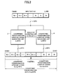
Claims (15)

  1. A logarithmic transformer comprising:
    a first bit string generating means (3) for generating a first bit string of binary data indicating the position of a highest order bit of logic "1" out of bits of digital data to be logarithmically transformed; and
    a second bit string generating means (4) for determining, from said digital data, a second bit string of order lower than said highest order bit of logic "1",
    the logarithmic transformer outputting logarithmic transformation data, which includes said first bit string as an integral part of a logarithmic transformation value resulting from a logarithmic transformation of said digital data and said second bit string as a fractional part of said logarithmic transformation value.
  2. The logarithmic transformer according to claim 1, wherein said first bit string generating means (3) comprises:
    a detecting unit (3a) for detecting the position of said highest order bit of logic "1" out of the bits of said digital data; and
    a generating unit (3b) for generating said first bit string based on a result of detection by said detecting unit (3a).
  3. The logarithmic transformer according to claim 2, wherein
       said detecting unit (3a) detects said highest order bit of logic "1" by decoding said digital data.
  4. The logarithmic transformer according to claim 2 or 3, wherein
       said generating unit (3b) contains pieces of binary data indicating the positions of the respective bits of said digital data, and selects one out of said pieces of binary data based on the result of detection by said detecting unit, thereby generating said binary data indicating the position of said highest order bit of logic "1."
  5. The logarithmic transformer according to claim 4, wherein said generating unit (3b) is composed of a switching circuit for selecting one out of said pieces of binary data, based on the result of detection by said detecting unit.
  6. The logarithmic transformer according to any one of claims 2 - 5, wherein said detecting unit (3a) comprises:
    a first logic circuit for outputting data for excluding a bit string lower than said highest order bit of logic "1" from the bits of said digital data; and
    a second logic circuit for removing the bit string excluded by said data from the bits of said digital data, thereby detecting said highest order bit of logic "1."
  7. The logarithmic transformer according to claim 6, wherein:
    said first logic circuit includes a plurality of OR gates for inputting respective bits of said digital data from a most significant bit to a least significant bit, said OR gates having their outputs and inputs cascaded in association with the most significant bit to the least significant bit; and
    said OR gates generate said data for excluding by performing OR operations between the outputs of said OR gates of higher order bits and the respective bits of said digital data.
  8. The logarithmic transformer according to claim 6 or 7, wherein
       said second logic circuit detects said highest order bit of logic "1" by performing AND operations between the respective bits of said digital data and said data for excluding.
  9. The logarithmic transformer according to any one of claims 1 - 8, wherein
       said second bit string generating means (4) determines, as said second bit string, a bit string of a predetermined number of bits including a bit following said highest order bit of logic "1" out of the bits of said digital data.
  10. The logarithmic transformer according to claim 9, wherein
       when the number of bits from the bit following said highest order bit to a least significant bit of said digital data falls short of said predetermined number, said second bit string generating means (4) appends as many bits as a shortfall to the least significant bit to generate, as said second bit string, a bit string of said predetermined number of bits.
  11. The logarithmic transformer according to claim 9 or 10, wherein said second bit string generating means (4) comprises:
    a second bit string extracting unit (4b) for inputting said digital data as successive bit strings each having said predetermined number of bits; and
    a second bit string selecting unit (4a) for making said second bit string extracting unit to extract, as said second bit string, a bit string of said predetermined number of bits having the bit following said highest order bit of logic "1" as a most significant bit of said bit string of said predetermined number.
  12. The logarithmic transformer according to claim 11, wherein
       said second bit string selecting unit (4a) detects said highest order bit of logic "1" by decoding said digital data.
  13. The logarithmic transformer according to claim 12, wherein
       said second bit string extracting unit (4b) extracts the bit string of said predetermined number of bits including the bit following said highest order bit as the most significant bit, based on the result of detection decoded by said second bit string selecting unit (4a).
  14. The logarithmic transformer according to any one of claims 11 - 13, wherein said second bit string extracting unit (4b) is composed of a switching circuit for extracting the bit string of said predetermined number of bits based on the result of detection by said second bit string selecting unit (4a).
  15. A method of logarithmic transformation comprising:
    a first bit string generating step of generating a first bit string of binary data indicating the position of a highest order bit of logic "1" out of bits of digital data to be logarithmically transformed; and
    a second bit string generating step of determining, from said digital data, a second bit string of order lower than said highest order bit of logic "1",
       wherein logarithmic transformation data on said digital data is generated by using said first bit string as an integral part of a logarithmic transformation value resulting from a logarithmic transformation of said digital data and said second bit string as a fractional part of said logarithmic transformation value.
EP03016797A 2002-07-23 2003-07-23 Logarithmic transformer and method of logarithmic transformation Withdrawn EP1385084A1 (en)

Applications Claiming Priority (2)

Application Number Priority Date Filing Date Title
JP2002214046 2002-07-23
JP2002214046A JP2004056642A (en) 2002-07-23 2002-07-23 Logarithmic converter and logarithmic conversion method

Publications (1)

Publication Number Publication Date
EP1385084A1 true EP1385084A1 (en) 2004-01-28

Family

ID=29997226

Family Applications (1)

Application Number Title Priority Date Filing Date
EP03016797A Withdrawn EP1385084A1 (en) 2002-07-23 2003-07-23 Logarithmic transformer and method of logarithmic transformation

Country Status (3)

Country Link
US (1) US20040153488A1 (en)
EP (1) EP1385084A1 (en)
JP (1) JP2004056642A (en)

Families Citing this family (2)

* Cited by examiner, † Cited by third party
Publication number Priority date Publication date Assignee Title
TW200532487A (en) * 2004-03-16 2005-10-01 Benq Corp Logarithm conversion method and apparatus of the same
CN100340972C (en) * 2005-06-07 2007-10-03 北京北方烽火科技有限公司 Method for implementing logarithm computation by field programmable gate array in digital auto-gain control

Citations (2)

* Cited by examiner, † Cited by third party
Publication number Priority date Publication date Assignee Title
DE2312128A1 (en) * 1973-03-10 1974-09-12 Dirk Dr Ing Rotthaus CIRCUIT ARRANGEMENT FOR DETERMINING THE DUAL LOGARITHM OF A BINARY NUMBER
JPS57174741A (en) * 1981-04-21 1982-10-27 Toshiba Corp Arithmetic circuit

Family Cites Families (8)

* Cited by examiner, † Cited by third party
Publication number Priority date Publication date Assignee Title
US4748577A (en) * 1982-02-02 1988-05-31 Motorola, Inc. Logarithmic data compression
US4626825A (en) * 1985-07-02 1986-12-02 Vlsi Technology, Inc. Logarithmic conversion apparatus
EP0572695A1 (en) * 1992-06-03 1993-12-08 International Business Machines Corporation A digital circuit for calculating a logarithm of a number
US5570310A (en) * 1994-12-05 1996-10-29 Motorola Inc. Method and data processor for finding a logarithm of a number
KR970016936A (en) * 1995-09-06 1997-04-28 엘리 와이스 Apparatus and method for determining top digit
JP2001296992A (en) * 2000-04-14 2001-10-26 Mitsubishi Electric Corp Logarithmic operation device and logarithmic operation method
US6587070B2 (en) * 2001-04-03 2003-07-01 Raytheon Company Digital base-10 logarithm converter
US6976043B2 (en) * 2001-07-30 2005-12-13 Ati Technologies Inc. Technique for approximating functions based on lagrange polynomials

Patent Citations (2)

* Cited by examiner, † Cited by third party
Publication number Priority date Publication date Assignee Title
DE2312128A1 (en) * 1973-03-10 1974-09-12 Dirk Dr Ing Rotthaus CIRCUIT ARRANGEMENT FOR DETERMINING THE DUAL LOGARITHM OF A BINARY NUMBER
JPS57174741A (en) * 1981-04-21 1982-10-27 Toshiba Corp Arithmetic circuit

Non-Patent Citations (2)

* Cited by examiner, † Cited by third party
Title
PATENT ABSTRACTS OF JAPAN vol. 007, no. 018 (P - 170) 25 January 1983 (1983-01-25) *
R. OBERMAN: "The J-K Gate", IEEE TRANSACTIONS ON COMPUTERS, vol. 25, no. 11, November 1976 (1976-11-01), IEEE INC. NEW YORK, NY, USA, pages 1156 - 1159, XP002256256, ISSN: 0018-9340 *

Also Published As

Publication number Publication date
JP2004056642A (en) 2004-02-19
US20040153488A1 (en) 2004-08-05

Similar Documents

Publication Publication Date Title
JP3016987B2 (en) Signal generating apparatus and method
US4163211A (en) Tree-type combinatorial logic circuit
US5535402A (en) System for (N•M)-bit correlation using N M-bit correlators
CN113366765B (en) Reduce latch count to save hardware area for dynamic Huffman table generation
EP0328063A2 (en) Absolute value calculating circuit having a single adder
US5008668A (en) Method and apparatus for encoding and decoding data in residue number system
JPH07177039A (en) Huffman coding / decoding device
Lee et al. $2^{n} $ pattern run-length for test data compression
JP3189876B2 (en) Variable length code decoding circuit
US5832037A (en) Method of compressing and expanding data
US8234320B1 (en) Bitwise comparator for selecting two smallest numbers from a set of numbers
US7548175B2 (en) Encoding apparatus, decoding apparatus, encoding method, computer readable medium storing program thereof, and computer data signal
JPH08339291A (en) Selection circuit of maximum value
Wu et al. Efficient test compression technique for SoC based on block merging and eight coding
JPH05134851A (en) Multiplier output method
JPS61216024A (en) Method and apparatus for performing range change with digital circuit
US7924179B2 (en) Variable-length code determining device and variable-length code decoding method
EP1385084A1 (en) Logarithmic transformer and method of logarithmic transformation
US6938062B1 (en) Apparatus and method for providing higher radix redundant digit lookup tables for recoding and compressing function values
Gao et al. FPGA bitstream compression and decompression based on LZ77 algorithm and BMC technique
US11831344B2 (en) Providing codewords
US20180316938A1 (en) Method and apparatus for k-th order exp-golomb binarization
Hameed et al. A new lossless method of Huffman coding for text data compression and decompression process with FPGA implementation
US7916048B2 (en) Encoding a gray code sequence for an odd length sequence
US6738792B1 (en) Parallel mask generator

Legal Events

Date Code Title Description
PUAI Public reference made under article 153(3) epc to a published international application that has entered the european phase

Free format text: ORIGINAL CODE: 0009012

AK Designated contracting states

Kind code of ref document: A1

Designated state(s): AT BE BG CH CY CZ DE DK EE ES FI FR GB GR HU IE IT LI LU MC NL PT RO SE SI SK TR

AX Request for extension of the european patent

Extension state: AL LT LV MK

17P Request for examination filed

Effective date: 20040116

17Q First examination report despatched

Effective date: 20040428

AKX Designation fees paid

Designated state(s): DE FR GB

STAA Information on the status of an ep patent application or granted ep patent

Free format text: STATUS: THE APPLICATION HAS BEEN WITHDRAWN

18W Application withdrawn

Effective date: 20041112