CROSS-REFERENCE TO RELATED APPLICATIONS
This application is based upon and claims the benefit of priority
from the prior Japanese Patent Application No. 2002-217213, filed on
July 25, 2002, the entire contents of which are incorporated herein by
reference.
BACKGROUND OF THE INVENTION
Field of the Invention
The present invention relates to a resist pattern thickening
material which is applied onto a resist pattern and thickens the resist
pattern, and which can form a fine space pattern exceeding exposure
limits of light sources of existing exposure devices ("space pattern" is
hereby defined as a hole, trench, recess, or any other empty space that
is formed by a developed (removed) resist). The present invention
also relates to a resist pattern, a process for forming the resist pattern,
a semiconductor device, and a process for manufacturing the
semiconductor device, all of which use the resist pattern thickening
material.
Description of the Related Art
Conventionally, in manufacturing a semiconductor device, a
hole pattern or a line-and-space pattern is formed by using a resist
material. In recent years, there has been much research and
development of techniques for thickening the resist pattern forming
the portions other than the holes in the hole pattern or the line
portions in the line-and-space pattern, so as to make the space pattern
corresponding to the hole portions in the hole pattern or to the space
portions in the line-and-space pattern (i.e., the space pattern formed
by the resist pattern) extremely fine. As space patterns have become
increasingly fine, the exposure light needed at the time of forming the
pattern has changed from lights such as visible light, laser light and
the like, to X-rays and electron beams. However, from the standpoint
of maintaining good mass produceability, there is a strong demand in
continuing to use light (e.g., visible light, laser light and the like) as the
exposure light when forming fine patterns. Thus, the development of
a method which can efficiently form fine patterns by using deep
ultraviolet light, which is light of a short wavelength, as the exposure
light has been desired.
Japanese Patent Application Laid-Open (JP-A) No. 10-73927
discloses a technique called RELACS for making a space pattern finer.
This technique can form a fine space pattern by using KrF (krypton
fluoride) excimer laser (wavelength: 248 nm) which is deep ultraviolet
light, as the exposure light of a photoresist (which will hereinafter
simply be called "resist"). In this technique, a resist pattern is formed
by exposing a resist (a positive resist or a negative resist) to light by
using a KrF (krypton fluoride) excimer laser (wavelength: 248 nm) as
the exposure light. Thereafter, by using a water-soluble resin
composition, an applied film is provided so as to cover the resist
pattern. The applied film and the resist pattern are made to interact
at the interface thereof by using the residual acid within the material
of the resist pattern, and the resist pattern is thickened. (Hereinafter,
this thickening of the resist pattern will be referred to upon occasion as
"swelling".) In this way, the distance between the resist patterns is
shortened, and a fine space pattern is formed. In accordance with
this technique, if a hole pattern is used for example, it is possible to
form a fine hole pattern exceeding the exposure limit.
In recent years, the practical application of ArF (argon fluoride)
excimer laser (wavelength: 193 nm) as the next-generation exposure
light in place of KrF (krypton fluoride) excimer laser (wavelength: 248
nm) has advanced. However, in the above-described technique, it is
not possible to use ArF excimer laser as the exposure light, instead of
KrF excimer laser. The reason for this is as follows. A resist which
is used for KrF excimer laser (hereinafter called a "KrF resist"), which
is used as the resist in the above-described technique, is an aromatic
resin compound such as a novolak resin, naphthoquinone diazide, or
the like. The aromatic rings contained in the aromatic resin
compound strongly absorb ArF excimer laser. Thus, even if KrF
excimer laser is merely replaced with ArF excimer laser as the
exposure light in the above-described technique, the ArF excimer laser
cannot pass through the film of the KrF resist. Thus, in the
above-described technique, when ArF excimer laser or light of an even
shorter wavelength is used as the exposure light, a KrF resist cannot be
used, and a resist which is used for an ArF excimer laser (hereinafter
called an "ArF resist") which does not contain aromatic rings must be
used.
However, using an ArF resist as the resist in the
above-described technique, a problem arises in that the resist pattern
cannot be thickened efficiently.
Therefore, the current situation is that there has not yet been
developed techniques such as materials, methods and the like which,
after forming a resist pattern by using ArF excimer laser as well as KrF
excimer laser as the exposure light, can form an applied film on the
resist pattern and thicken the resist pattern. The development of
such techniques has been desired.
SUMMARY OF THE INVENTION
An object of the present invention is to provide a resist pattern
thickening material which, when applied on a resist pattern, can
efficiently thicken the resist pattern, and which is suited to formation
of a fine space pattern, exceeding the exposure limits of light sources
of existing exposure devices.
Another object of the present invention is to provide a process
for forming a resist pattern which, when patterning a resist pattern,
can utilize, as is, light sources (such as ArF excimer laser light or the
like) of existing exposure devices, and which has excellent mass
productivity, and which can form a space pattern finely, exceeding the
exposure limits of such light sources, and to provide a resist pattern
formed by this process for forming a resist pattern.
Yet another object of the present invention is to provide a
process for manufacturing a semiconductor device which, by using a
fine space pattern formed by the resist pattern, can form a fine pattern
on an underlying layer which is an oxide film or the like, and which
can efficiently mass produce high-performance semiconductor devices
having fine wiring and the like, and to provide a high-performance
semiconductor device manufactured by this process for manufacturing
a semiconductor device.
The resist pattern thickening material of the present invention
comprises: a resin; a crosslinking agent; and at least one of a cationic
surfactant, an amphoteric surfactant, and a non-ionic surfactant
selected from an alkoxylate surfactant, a fatty acid ester surfactant, an
amide surfactants, an alcohol surfactants, and an ethylene diamine
surfactant.
The resist pattern of the present invention is formed by, after a
resist pattern is formed, the resist pattern thickening material of the
present invention being applied so as to cover a surface of the resist
pattern.
In the process for forming a resist pattern of the present
invention, after a resist pattern is formed, the resist pattern thickening
material of the present invention is applied so as to cover a surface of
the resist pattern.
The semiconductor device of the present invention has a
pattern formed by using the resist pattern thickening material of the
present invention.
The process for manufacturing a semiconductor device of the
present invention comprises steps of: applying a resist pattern
thickening material to cover a surface of a resist pattern to be
thickened, after forming the resist pattern to be thickened on an
underlying layer, so as to thicken the resist pattern to be thickened and
form a resist pattern; and etching the underlying layer using the resist
pattern as a mask so as to pattern the underlying layer.
BRIEF DESCRIPTION OF THE DRAWINGS
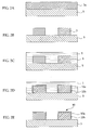
FIGs. 1A to 1C are schematic diagrams for explaining one
example of the mechanism of thickening a resist pattern by using a
resist pattern thickening material of the present invention.
FIGs. 2A to 2E are schematic diagrams for explaining one
example of a process for forming a resist pattern of the present
invention.
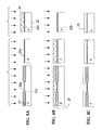
FIGs. 3A to 3B are top views for explaining a FLASH EPROM
which is one example of a semiconductor device of the present
invention.
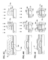
FIGs. 4A to 4C are part 1 of a set of cross-sectional schematic
diagrams for explaining a process for manufacturing the FLASH
EPROM which is one example of a process for manufacturing a
semiconductor device of the present invention.
FIGs. 5D to 5F are part 2 of the set of cross-sectional schematic
diagrams for explaining the process for manufacturing the FLASH
EPROM which is one example of the process for manufacturing a
semiconductor device of the present invention.
FIGs. 6G to 6I are part 3 of the set of cross-sectional schematic
diagrams for explaining the process for manufacturing the FLASH
EPROM which is one example of the process for manufacturing a
semiconductor device of the present invention.
FIGs. 7A to 7C are cross-sectional schematic diagrams for
explaining a process for manufacturing a FLASH EPROM which is
another example of a process for manufacturing a semiconductor
device of the present invention.
FIGs. 8A to 8C are cross-sectional schematic diagrams for
explaining a process for manufacturing a FLASH EPROM which is
another example of a process of manufacturing a semiconductor
device of the present invention.
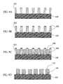
FIGs. 9A to 9D are cross-sectional schematic diagrams for
explaining one example in which a resist pattern, which has been
thickened by using the resist pattern thickening material of the present
invention, is applied to the manufacturing of a recording head.
FIGs. 10A to 10B are cross-sectional schematic diagrams for
explaining part 1 and 2 of a process of another example in which a
resist pattern, which has been thickened by using the resist pattern
thickening material of the present invention, is applied to the
manufacturing of a recording head.
FIGs. 11C to 11D are cross-sectional schematic diagrams for
explaining part 3 and 4 of the process of the other example in which
the resist pattern, which has been thickened by using the resist pattern
thickening material of the present invention, is applied to the
manufacturing of the recording head.
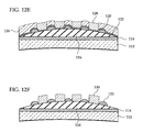
FIGs. 12E to 12F are cross-sectional schematic diagrams for
explaining part 5 and 6 of the process of the other example in which
the resist pattern, which has been thickened by using the resist pattern
thickening material of the present invention, is applied to the
manufacturing of the recording head.
FIG. 13 is a plan view showing one example of the recording
head manufactured by the processes of FIGs.10A through 12F.
DESCRIPTION OF THE PREFERRED EMBODIMENTS
(Resist Pattern Thickening Material)
The resist pattern thickening material of the present invention
comprises a resin; a crosslinking agent; and at least one of a cationic
surfactant, an amphoteric surfactant, and a non-ionic surfactants
selected from an alkoxylate surfactant, a fatty acid ester surfactant, an
amide surfactant, an alcohol surfactant, and an ethylene diamine
surfactant. As needed, the resist pattern thickening material may also
include a water-soluble aromatic compound, a resin containing an
aromatic compound in a portion thereof, an organic solvent, and/or
other components which are appropriately selected.
When the resist pattern thickening material of the present
invention is applied on an initial resist pattern (which may be also
referred as "a resist pattern to be thickened" hereinafter), the portion
of the applied resist pattern thickening material which is in a vicinity
of the interface with the initial resist pattern (the resist pattern to be
thickened) seeps into the initial resist pattern (the resist pattern to be
thickened) and crosslinks with the material of the initial resist pattern
(the resist pattern to be thickened). At this time, because the affinity
of the resist pattern thickening material and the initial resist pattern
(the resist pattern to be thickened) is good, a surface layer, in which
the resist pattern thickening material and the initial resist pattern (the
resist pattern to be thickened) have become integral, is efficiently
formed on the surface of the initial resist pattern (the resist pattern to
be thickened), so that the initial resist pattern (the resist pattern to be
thickened) becomes an inner layer. (Namely, the resist pattern to be
thickened is efficiently thickened by the resist pattern thickening
material.) The resist pattern which is formed in this way has been
thickened by the resist pattern thickening material. Thus, a space
pattern formed by the resist pattern exceeds exposure limits and has
an even more fine structure.
The resist pattern thickening material of the present invention
is water-soluble or alkali-soluble.
The resist pattern thickening material of the present invention
may be an aqueous solution, a colloid liquid or an emulsion liquid or
the like. Of these, an aqueous solution is preferable.
-Resin-
The resin is not particularly limited, and can be appropriately
selected in accordance with the object. However, it is preferable that
the resin is water-soluble or alkali-soluble. It is more preferable that
the resin can generate a crosslinking reaction, or that the resin cannot
generate a crosslinking reaction but can mix together with a
water-soluble crosslinking agent. Examples thereof include
polyvinyl alcohol, polyvinyl acetal, polyvinyl acetate, polyacrylic acid,
polyvinyl pyrrolidone, polyethyleneimine, polyethylene oxide, styrene
- maleic acid copolymer, polyvinyl amine, polyaryl amine, oxazoline
group containing water-soluble resins, water-soluble melamine resins,
water-soluble urea resins, alkyd resins, sulfonamide resins, and the
like.
These may be used singly, or in combination of two or more.
Among these, polyvinyl alcohol, polyvinyl acetal, polyvinyl acetate,
and the like are preferable. In the present invention, it is preferable
that the resin contains polyvinyl acetal. From the standpoint of being
able to easily change the solubility by the crosslinking, the resin more
preferably contains polyvinyl acetal in an amount of 5% by mass to
40% by mass.
The content of the resin in the resist pattern thickening material
differs in accordance with the type, the content and the like of the
crosslinking agent, the water-soluble aromatic compound and the like,
and cannot be stipulated unconditionally, and can be appropriately
selected in accordance with the object.
-Crosslinking Agent-
The crosslinking agent is not particularly limited, and can be
appropriately selected in accordance with the object. However,
water-soluble crosslinking agents which cause crosslinking due to heat
or an acid are preferable. Amino crosslinking agents are suitable
examples.
Suitable examples of the amino crosslinking agents are
melamine derivatives, urea derivatives, uril derivatives, and the like.
These may be used singly, or in combination of two or more.
Examples of the urea derivatives include urea,
alkoxymethylene urea, N-alkoxymethylene urea, ethylene urea,
ethylene urea carboxylic acid, derivatives thereof, and the like.
Examples of the melamine derivatives include alkoxymethyl
melamine, derivatives thereof, and the like.
Examples of the uril derivatives include benzoguanamine,
glycol uril, derivatives thereof, and the like.
The content of the crosslinking agent in the resist pattern
thickening material differs in accordance with the type, the content
and the like of the resin and the like, and cannot be stipulated
unconditionally, and can be appropriately selected in accordance with
the object.
-Cationic Surfactant-
The cationic surfactant is not particularly limited and can be
appropriately selected in accordance with the object. Examples
thereof include alkyl cationic surfactants, amide type quaternary
cationic surfactants, ester type quaternary cationic surfactants, and the
like.
-Amphoteric Surfactant-
The amphoteric surfactant is not particularly limited and can be
appropriately selected in accordance with the object. Examples
thereof include amine oxide surfactants, betaine surfactants, and the
like.
-Non-Ionic Surfactant-
Suitable examples of non-ionic surfactants include surfactants
selected from among alkoxylate surfactants, fatty acid ester surfactants,
amide surfactants, alcohol surfactants, and ethylene diamene
surfactants. Specific examples thereof include polyoxyethylene -
polyoxypropylene condensation products, polyoxyalkylene alkylether
compounds, polyoxyethylene alkylether compounds, polyoxyethylene
derivatives, sorbitan fatty acid ester compounds, glycerin fatty acid
ester compounds, primary alcohol ethoxylate compounds, phenol
ethoxylate compounds, and nonylphenol ethoxylate surfactants,
octylphenol ethoxylate surfactants, lauryl alcohol ethoxylate
surfactants, oleyl alcohol ethoxylate surfactnts, fatty acid ester
surfactants, amide surfactants, natural alcohol surfactants, ethylene
diamine surfactants, and secondary alcohol ethoxylate surfactants, and
the like.
These may be used singly, or in combination of two or more.
The content of the surfactant in the resist pattern thickening material
can be appropriately selected in accordance with the type, the content,
and the like of the resin, the crosslinking agent and the like.
-Water-Soluble Aromatic Compound-
From the standpoint of markedly improving the etching
resistance of the obtained resist pattern, the resist pattern thickening
material preferably contains a water-soluble aromatic compound.
The water-soluble aromatic compound is not particularly
limited provided that it is an aromatic compound and exhibits water
solubility, and can be appropriately selected in accordance with the
object. However, water-soluble aromatic compounds exhibiting
water solubility of 1 g or more in 100 g of water of 25°C are preferable,
those exhibiting water solubility of 3 g or more in 100 g of water of
25°C are more preferable, and those exhibiting water solubility of 5 g
or more in 100 g of water of 25°C are particularly preferable.
Examples of the water-soluble aromatic compounds are
polyphenol compounds, aromatic carboxylic acid compounds,
naphthalene polyhydroxy compounds, benzophenone compounds,
flavonoid compounds, porphin, water-soluble phenoxy resins,
aromatic-containing water-soluble dyes, derivatives thereof,
glycosides thereof, and the like. These may be used singly, or in
combination of two or more.
Examples of the polyphenol compounds and derivatives
thereof include catechin, anthocyanidin (pelargonidin-type
(4'-hydroxy), cyanidin-type (3',4'-dihydroxy), delphinidin-type
(3',4',5'-trihydroxy)), flavan-3,4-diol, proanthocyanidin, resorcinol,
resorcinol [4] arene, pyrogallol, gallic acid, derivatives and glycosides
thereof, and the like.
Examples of the aromatic carboxylic acid compounds and
derivatives thereof include salicylic acid, phthalic acid, dihydroxy
benzoic acid, tannin, derivatives and glycosides thereof, and the like.
Examples of the naphthalene polyhydroxy compounds and
derivatives thereof include naphthalene diol, naphthalene triol,
derivatives and glycosides thereof, and the like.
Examples of the benzophenone compounds and derivatives
thereof include alizarin yellow A, derivatives and glycosides thereof,
and the like.
Examples of the flavonoid compounds and derivatives thereof
include flavone, isoflavone, flavanol, flavonone, flavonol, flavan-3-ol,
aurone, chalcone, dihydrochalcone, quercetin, derivatives and
glycosides thereof, and the like.
Among the aforementioned water-soluble aromatic compounds,
from the standpoint of excellent water solubility, those having two or
more polar groups are preferable, those having three or more polar
groups are more preferable, and those having four or more polar
groups are particularly preferable.
The polar groups are not particularly limited, and may be
appropriately selected in accordance with the object. Examples
include hydroxyl group, carboxyl group, carbonyl group, sulfonyl
group, and the like.
The content of the water-soluble aromatic compound in the
resist pattern thickening material can be appropriately determined in
accordance with the type, the content, and the like of the resin, the
crosslinking agent, and the like.
-Resin Containing an Aromatic Compound in a Portion Thereof-
From the standpoint of markedly improving the etching
resistance of the obtained resist pattern, it is preferable that the resist
pattern thickening material contains a resin containing an aromatic
compound in a portion thereof.
The resin containing an aromatic compound in a portion
thereof is not particularly limited and can be appropriately selected in
accordance with the object. However, those which can generate a
crosslinking reaction are preferable. Suitable examples include
polyvinyl aryl acetal resins, polyvinyl aryl ether resins, polyvinyl aryl
ester resins, and derivatives thereof. It is preferable to use at least
one selected therefrom. From the standpoint of exhibiting water
solubility or alkali solubility to an appropriate degree, such a resin
which contains an acetyl group is more preferable. These may be
used singly, or in combination of two or more.
The polyvinyl aryl acetal resin is not particularly limited and
may be appropriately selected in accordance with the object.
Examples thereof include β-resorcinol acetal and the like.
The polyvinyl aryl ether resin is not particularly limited and
may be appropriately selected in accordance with the object.
Examples thereof include 4-hydroxybenzyl ether and the like.
The polyvinyl aryl ester resin is not particularly limited and
may be appropriately selected in accordance with the object.
Examples thereof include benzoate and the like.
The method of producing the polyvinyl aryl acetal resin is not
particularly limited and may be appropriately selected in accordance
with the object. A suitable example is a known method of producing
using a polyvinyl acetal reaction, or the like. Such a producing
method is a method in which, for example, polyvinyl alcohol, and
aldehyde in an amount needed stoichiometrically for the polyvinyl
alcohol are made to undergo an acetalizing reaction in the presence of
an acid catalyst. Specifically, suitable examples are the methods
disclosed in USP Nos. 5,169,897 and 5,262,270, JP-A No. 5-78414, and
the like.
The method of producing the polyvinyl aryl ether resin is not
particularly limited and may be appropriately selected in accordance
with the object. Examples thereof are a copolymerization reaction of
a corresponding vinyl aryl ether monomer and vinyl acetate; an
etherizing reaction of polyvinyl alcohol and an aromatic compound
having a halogenated alkyl group in the presence of a basic catalyst
(the ether synthesizing reaction of Williamson); and the like.
Specifically, suitable examples are the methods disclosed in JP-A Nos.
2001-40086, 2001-181383, 6-116194, and the like.
The method of producing the polyvinyl aryl ester resin is not
particularly limited and may be appropriately selected in accordance
with the object. Examples thereof are a copolymerization reaction of
a corresponding vinyl aryl ester monomer and vinyl acetate; an
esterizing reaction of polyvinyl alcohol and an aromatic carboxylic
acid halide compound in the presence of a basic catalyst; and the like.
The aromatic compound in the resin containing an aromatic
compound in a portion thereof is not particularly limited, and may be
appropriately selected in accordance with the object. Suitable
examples include monocyclic aromatic compounds such as benzene
derivatives, pyridine derivatives, and the like, and compounds in
which a plurality of aromatic rings are connected (polycyclic aromatic
compounds such as naphthalene, anthracene, and the like), and the
like.
From the standpoint of appropriate water solubility, the
aromatic compound in the resin containing an aromatic compound in
a portion thereof preferably contains at least one functional group
such as hydroxyl group, cyano group, alkoxyl group, carboxyl group,
amino group, amide group, alkoxylcarbonyl group, hydroxyalkyl
group, sulfonyl group, acid anhydride group, lactone group, cyanate
group, isocyanate group, ketone group or the like, or a sugar
derivative. It is more preferable for the aromatic compound to
contain at least one functional group selected from hydroxyl group,
amino group, sulfonyl group, carboxyl group, and derivatives thereof.
The molar content of the aromatic compound in the resin
containing an aromatic compound in a portion thereof is not
particularly limited provided that it does not affect the etching
resistance, and can be appropriately selected in accordance with the
object. However, when high etching resistance is required, the molar
content is preferably 5 mol% or more, and 10 mol% or more is more
preferable.
Note that the molar content of the aromatic compound in the
resin containing an aromatic compound in a portion thereof can be
measured by using NMR or the like for example.
The content, in the resist pattern thickening material, of the
resin containing an aromatic compound in a portion thereof, can be
appropriately determined in accordance with the type, the content and
the like of the resin, the crosslinking agent, and the like.
-Organic Solvent-
By making the resist pattern thickening material contain an
organic solvent, the solubility of the resin, the crosslinking agent, the
water-soluble aromatic compound, the resin containing an aromatic
compound in a portion thereof, and the like in the resist pattern
thickening material can be improved.
The organic solvent is not particularly limited, and can be
appropriately selected in accordance with the object. Examples
thereof include alcohol organic solvents, chain ester organic solvents,
cyclic ester organic solvents, ketone organic solvents, chain ether
organic solvents, cyclic ether organic solvents and the like.
Examples of the alcohols are methanol, ethanol, propyl alcohol,
isopropyl alcohol, butyl alcohol, and the like.
Examples of the chain esters are ethyl lactate, propylene glycol
methyl ether acetate (PGMEA), and the like.
Examples of the cyclic esters are lactone organic solvents such
as γ-butyrolactone, and the like.
Examples of the ketones are acetone, cyclohexanone, heptanone,
and the like.
Examples of the chain ethers are ethylene glycol dimethylether,
and the like.
Examples of the cyclic ethers are tetrahydrofuran, dioxane, and
the like.
These may be used singly, or in combination of two or more.
Thereamong, organic solvents having a boiling point of around 80°C
to 200°C are preferable from the standpoint of carrying out thickening
accurately.
The content of the organic solvent in the resist pattern
thickening material can be appropriately determined in accordance
with the type, the content, and the like of the resin, the crosslinking
agent, the water-soluble aromatic compound, the resin containing an
aromatic compound in a portion thereof, the surfactant, and the like.
-Other Components-
The other components are not particularly limited provided
that they do not adversely affect the effects of the present invention,
and can be appropriately selected in accordance with the object.
Examples thereof are various types of known additives such as
thermal acid generating agents, quenchers such as amine type, amide
type, ammonium chloride type quenchers, and the like.
The content of the other components in the resist pattern
thickening material can be appropriately determined in accordance
with the type, the content and the like of the resin, the surfactant, the
crosslinking agent, the water-soluble aromatic compound, the resin
containing an aromatic compound in a portion thereof, the organic
solvent, and the like.
-Use-
The resist pattern thickening material can be used by being
applied onto the resist pattern to be thickened.
At the time of applying, the surfactant may be applied before
applying of the resist pattern thickening material, in which no
surfactant is contained, or in which a surfactant is further contained.
When the resist pattern thickening material is applied onto and
crosslinks with the resist pattern to be thickened, the resist pattern to
be thickened thickens. A surface layer having excellent etching
resistance is formed on the resist pattern to be thickened, and a resist
pattern is formed. As a result, the diameter or width of a space
pattern formed by the resist pattern is smaller than that of the former
space pattern. Therefore an even finer space pattern is formed
exceeding the exposure limit of the light source of the exposure device,
which is used at the time of patterning the resist pattern to be
thickened. In a case in which ArF excimer laser light is used at the
time of patterning a resist pattern to be thickened, for example, when
the obtained resist pattern to be thickened is thickened by using the
resist pattern thickening material so as to form a resist pattern, a space
pattern formed by the resist pattern is a fine space pattern which is
similar to that obtained when patterning by using an electron beam.
It should be noted that, at this time, the amount of thickening of
the resist pattern can be controlled to a desired degree by
appropriately adjusting the viscosity of the resist pattern thickening
material, the applying thickness of the resist pattern thickening
material, the baking temperature, the baking time, and the like.
-Material of Resist Pattern to be Thickened-
The material of the resist pattern to be thickened (the resist
pattern on which the resist pattern thickening material of the present
invention is applied) is not particularly limited, and can be
appropriately selected from among known resist materials in
accordance with the object. The resist pattern to be thickened may be
either of a negative type or a positive type resist pattern. Suitable
examples thereof include g-line resists, i-line resists, KrF resists, ArF
resists, F2 resists, electron beam resists, and the like, which can be
patterned by g-line, i-line, KrF excimer lasers, ArF excimer lasers, F2
excimer lasers, electron beams, and the like, respectively. These
resists may be chemically amplified types, or non-chemically
amplified types. Among these, KrF resists, ArF resists, and the like
are preferable, and ArF resists are more preferable.
The material of the resist pattern to be thickened is not
particularly limited, and can be appropriately selected in accordance
with the object. Examples thereof include novolak resists,
polyhydroxystyrene (PHS) resists, acrylic resists, cycloolefin-maleic
acid anhydride (COMA) resists, cycloolefin resists, hybrid (alicyclic
acryl-COMA copolymer) resists, and the like. These materials may
be fluorine-modified or the like.
The method of forming the resist pattern to be thickened, and
the size, the thickness and the like of the resist pattern to be thickened
are not particularly limited, and can be appropriately selected in
accordance with the object. In particular, the thickness can be
appropriately determined by the underlying layer which is the object
of working, the etching conditions, and the like. However, the
thickness is generally about 0.2 µm to 200 µm.
The thickening of the resist pattern to be thickened by using the
resist pattern thickening material of the present invention will be
described hereinafter with reference to the drawings.
As shown in FIG. 1A, after a resist pattern (a resist pattern to be
thickened) 3 has been formed on an underlying layer (base) 5, a resist
pattern thickening material 1 is applied onto the surface of the resist
pattern (the resist pattern to be thickened) 3. Prebaking (heating and
drying) is carried out, so that a film is formed. Then, mixing
(impregnating) of the resist pattern thickening material 1 into the resist
pattern (the resist pattern to be thickened) 3 occurs at the interface
between the resist pattern (the resist pattern to be thickened) 3 and the
resist pattern thickening material 1.
Here, as shown in FIG. 1B, when crosslinking baking (a
crosslinking reaction) is carried out at a higher temperature than the
temperature of the prebaking (heating and drying), the mixed
(impregnated) portion at the interface of the resist pattern (the resist
pattern to be thickened) 3 and the resist pattern thickening material 1
crosslinks.
Thereafter, as shown in FIG. 1C, by carrying out developing
processing, the portions, among the applied resist pattern thickening
material 1, which have not crosslinked with the resist pattern (the
resist pattern to be thickened) 3 or at which the crosslinking is weak
(portions having high water solubility) are dissolved and removed, so
that a resist pattern 10 is formed (developed).
The developing processing may be carried out in water or a
weak alkali aqueous solution. However, water developing is
preferable from the standpoint that the developing processing can be
carried out efficiently at a low cost.
The resist pattern 10 has, on a surface of a resist pattern 10b (the
resist pattern 3), a surface layer 10a which has been formed by the
resist pattern thickening material 1 crosslinking on the resist pattern
(the resist pattern to be thickened) 3. The resist pattern 10 is thicker
than the resist pattern (the resist pattern to be thickened) 3 by an
amount corresponding to the thickness of the surface layer 10a. Thus,
the width of a space pattern formed by the resist pattern 10 is smaller
than that of the former space pattern (the resist pattern to be
thickened) 3, and the space pattern formed by the resist pattern 10 is
particularly fine.
The surface layer 10a of the resist pattern 10 is formed by the
resist pattern thickening material 1. In a case in which the resist
pattern thickening material 1 contains at least one of an aromatic
compound and a resin containing an aromatic compound in a portion
thereof, even if the resist pattern (the resist pattern to be thickened) 3 is
a material which has poor etching resistance, the resist pattern 10,
which has on the surface thereof the surface layer 10a having excellent
etching resistance, has markedly excellent etching resistance.
-Applications-
The resist pattern thickening material of the present invention
can suitably be used in thickening a resist pattern which, at the time of
patterning, can use not only KrF excimer laser light, but also ArF
excimer laser light. Further, when the resist pattern thickening
material contains at least one of an aromatic compound and a resin
containing an aromatic compound in a portion thereof, the resist
pattern thickening material can more suitably be used in covering and
thickening patterns which are exposed to plasma or the like and which
are formed of resin or the like whose surface etching resistance must
be improved, and can particularly suitably be used in the resist pattern
and the process for forming the same of the present invention, and in
the semiconductor device and the process for manufacturing the same
of the present invention.
(Resist Pattern)
The resist pattern of the present invention is the thickened resist
pattern, and has a surface layer on the initial resist pattern (the resist
pattern to be thickened). Thus, the resist pattern of the present
invention is suitable for the formation of fine patterns, and an ArF
excimer laser can be used as the exposure light when forming the
resist pattern.
The surface layer preferably has excellent etching resistance. It
is preferable that the etching rate (nm/min) of the surface layer is
equivalent to or greater than that of the resist pattern to be thickened
which exists at the inner side of the surface layer. Specifically, when
measurement is carried out under the same conditions, the ratio (resist
pattern to be thickened/surface layer) of the etching rate (nm/min) of
the surface layer and the etching rate (nm/min) of the resist pattern to
be thickened is preferably 1.1 or more, and is more preferably 1.2 or
more, and is particularly preferably 1.3 or more.
The etching rate (nm/min) can be measured by, for example,
carrying out etching processing for a predetermined time by using a
known etching device, measuring the amount of film reduction of the
sample, and determining the amount of film reduction per unit time.
The surface layer can suitably be formed by using the resist
pattern thickening material of the present invention. From the
standpoint of improving the etching resistance, the surface layer
preferably contains at least one of an aromatic compound or a resin
containing an aromatic compound in a portion thereof.
Whether the surface layer does or does not contain at least one
of an aromatic compound and a resin containing an aromatic
compound in a portion thereof, can be confirmed by, for example,
analyzing the IR absorption spectrum of the surface layer.
The resist pattern may partially contain at least one of an
aromatic compound and a resin containing an aromatic compound in
a portion thereof, and such an aspect is preferable from the standpoint
of underlying layer workability. In this case, the content of the at
least one of the aromatic compound and the resin containing an
aromatic compound in a portion thereof can be set so as to gradually
decrease from the surface layer toward the inner portion.
In the resist pattern of the present invention, the border
between the resist pattern to be thickened and the surface layer may be
clear, or may be unclear.
The resist pattern of the present invention can preferably be
formed by the process for forming a resist pattern of the present
invention which will be described hereinafter.
The resist pattern of the present invention can suitably be used
in, for example, the manufacturing of functional parts such as mask
patterns, reticle patterns, recording heads, LCDs (liquid crystal
displays), PDPs (plasma display panels), SAW filters (surface acoustic
wave filters), and the like; optical parts used in connecting optical
wiring; fine parts such as microactuators and the like; semiconductor
devices; and the like. The resist pattern can be particularly preferably
used in the manufacturing of the semiconductor device of the present
invention which will be described hereinafter.
(Process for forming Resist Pattern)
In the process for forming a resist pattern of the present
invention, after a resist pattern to be thickened is formed, the resist
pattern thickening material of the present invention is applied so as to
cover the surface of the resist pattern to be thickened.
Suitable examples of materials of the resist pattern to be
thickened are the materials which were listed above in the discussion
of the resist pattern thickening material of the present invention.
The resist pattern to be thickened can be formed in accordance
with known methods.
The resist pattern to be thickened can be formed on an
underlying layer (a base). The underlying layer (base) is not
particularly limited, and can be appropriately selected in accordance
with the object. However, when the resist pattern to be thickened is
formed on a semiconductor device, the underlying layer (base) is a
substrate such as a silicon wafer or the like.
The method of applying the resist pattern thickening material is
not particularly limited, and can be appropriately selected from
among known applying methods in accordance with the object.
Suitable examples are a spin coating method and the like. In the case
in which a spin coating method is used, the conditions are as follows
for example: the rotational speed is about 100 rpm to 10,000 rpm, and
is preferably 800 rpm to 5,000 rpm, and the time is about one second to
10 minutes, and is preferably one second to 90 seconds.
The applied thickness at the time of applying is usually about
10 nm (100 Å) to about 1,000 nm (10,000 Å), and is preferably about
100 nm (1,000 Å) to 500 nm (5,000 Å).
It should be noted that, at the time of applying, the surfactant
may be applied before applying of the resist pattern thickening
material, without being contained in the resist pattern thickening
material.
Carrying out prebaking (heating and drying) of the applied
resist pattern thickening material during applying or after applying is
preferable from the standpoint that the resist pattern thickening
material can be efficiently mixed (impregnated) into the resist pattern
to be thickened at the interface between the resist pattern to be
thickened and the resist pattern thickening material.
The conditions, the method and the like of the prebaking
(heating and drying) are not particularly limited and can be
appropriately selected in accordance with the object, provided that
they do not cause softening of the resist pattern to be thickened. For
example, the temperature is about 40°C to about 120°C, and is
preferably 70°C to 100°C, and the time is about 10 seconds to about 5
minutes, and is preferably 40 seconds to 100 seconds.
Carrying out crosslinking baking (a crosslinking reaction) of the
applied resist pattern thickening material after the prebaking (heating
and drying) is preferable from the standpoint that the crosslinking
reaction of the mixed (impregnated) portion at the interface between
the resist pattern to be thickened and the resist pattern thickening
material can be made to proceed efficiently.
The conditions, the method and the like of the crosslinking
baking (the crosslinking reaction) are not particularly limited and can
be appropriately selected in accordance with the object. However,
usually, a temperature higher than that during the prebaking (heating
and drying) is used. The conditions of the crosslinking baking (the
crosslinking reaction) are, for example, the temperature is about 70°C
to about 150°C, and is preferably 90°C to 130°C, and the time is about
10 seconds to about 5 minutes, and is preferably 40 seconds to 100
seconds.
Carrying out developing processing of the applied resist
pattern thickening material after the crosslinking baking (the
crosslinking reaction) is preferable from the standpoint that, among
the applied resist pattern thickening material, the portions thereof
which have not crosslinked with the resist pattern to be thickened and
the portions thereof at which the crosslinking is weak (the portions
having high water solubility) are dissolved and removed, so that the
resist pattern of the present invention, which is formed in a thickened
state, can be developed.
The same comments as those above regarding developing
processing are applicable here as well.
The process for forming the resist pattern of the present
invention will be described hereinafter with reference to the drawings.
As shown in FIG. 2A, after a resist material (a material for a
resist pattern to be thickened) 3a is applied onto the underlying layer
(base) 5, as shown in FIG. 2B, the resist material (the material for a
resist pattern to be thickened) 3a is patterned so that a resist pattern (a
resist pattern to be thickened) 3 is formed. Thereafter, as shown in
FIG. 2C, the resist pattern thickening material 1 is applied onto the
surface of the resist pattern (the resist pattern to be thickened) 3, and
prebaking (heating and drying) is carried out so that a film is formed.
Then, mixing (impregnating) of the resist pattern thickening material 1
into the resist pattern (the resist pattern to be thickened) 3 takes place
at the interface between the resist pattern (the resist pattern to be
thickened) 3 and the resist pattern thickening material 1.
Here, as shown in FIG. 2D, when crosslinking baking (a
crosslinking reaction) is carried out at a temperature which is higher
than that of the prebaking (heating and drying), the mixed
(impregnated) portion at the interface of the resist pattern (to be
thickened) 3 and the resist pattern thickening material 1 crosslinks.
Thereafter, as shown in FIG. 2E, by carrying out developing
processing, among the applied resist pattern thickening material 1, the
portions thereof which have not crosslinked with the resist pattern
(the resist pattern to be thickened) 3 and the portions thereof at which
the crosslinking is weak (the portions having high water solubility) are
dissolved and removed, so that a resist pattern 10 having the surface
layer 10a on the resist pattern 10b (the resist pattern 3) is formed
(developed).
The developing processing may be carried out in water or a
weak alkali aqueous solution. However, water developing is
preferable from the standpoint that the developing processing can be
carried out efficiently at a low cost.
The resist pattern 10 has, on a surface of the resist pattern 10b
(the resist pattern 3), the surface layer 10a which has been formed by
the resist pattern thickening material 1 crosslinking on the resist
pattern (the resist pattern to be thickened) 3. The resist pattern 10 is
made thicker than the resist pattern (the resist pattern to be thickened)
3 by an amount corresponding to the thickness of the surface layer 10a.
Thus, the width of a space pattern formed by the resist pattern 10 is
smaller than that of the former space pattern (the resist pattern to be
thickened) 3, and the space pattern formed by the resist pattern 10 is
particularly fine.
The surface layer 10a of the resist pattern 10 is formed by the
resist pattern thickening material 1. In a case in which the resist
pattern thickening material 1 contains at least one of an aromatic
compound and a resin containing an aromatic compound in a portion
thereof, even if the resist pattern (the resist pattern to be thickened) 3 is
a material which has poor etching resistance, the resist pattern 10,
which has on the surface thereof the surface layer 10a having excellent
etching resistance, is a structure whose etching resistance is markedly
excellent.
The resist pattern which is formed by the process for forming a
resist pattern of the present invention is the resist pattern of the
present invention. The resist pattern has, on the surface of the resist
pattern to be thickened, a surface layer which is formed by the resist
pattern thickening material of the present invention crosslinking on
the resist pattern to be thickened. When the resist pattern thickening
material contains at least one of an aromatic compound and a resin
containing an aromatic compound in a portion thereof, even if the
resist pattern to be thickened is a material having poor etching
resistance, the resist pattern, which has the surface layer having
excellent etching resistance on the surface of the resist pattern to be
thickened, can efficiently be formed. Further, the resist pattern which
is formed by the process for forming a resist pattern of the present
invention is made thicker than the resist pattern to be thickened by an
amount corresponding to the thickness of the surface layer.
Therefore, the diameter or the width of a space pattern formed by the
resist pattern is smaller than those of the former space pattern formed
by the resist pattern to be thickened. Therefore, in accordance with
the process for forming a resist pattern of the present invention, a fine
space pattern can be formed efficiently.
The resist pattern formed by the process for forming a resist
pattern of the present invention can suitably be used in, for example,
the manufacturing of functional parts such as mask patterns, reticle
patterns, recording heads, LCDs (liquid crystal displays), PDPs
(plasma display panels), SAW filters (surface acoustic wave filters),
and the like; optical parts used in connecting optical wiring; fine parts
such as microactuators and the like; semiconductor devices; and the
like. The resist pattern can be particularly preferably used in the
manufacturing of the semiconductor device of the present invention
which will be described hereinafter.
(Semiconductor Device and Process for Manufacturing Semiconductor
Device)
The semiconductor device of the present invention is not
particularly limited, provided that it is manufactured by using the
resist pattern thickening material of the present invention, and that it
has a fine pattern (a wiring pattern or the like) formed by the resist
pattern of the present invention. The semiconductor device has
known members and the like which are appropriately selected as
needed.
Specific examples of the semiconductor device of the present
invention are flash memories, DRAMs, FRAMs, and the like.
The semiconductor device of the present invention can suitably
be manufactured by the process for manufacturing a semiconductor
device of the present invention.
The process for manufacturing a semiconductor device of the
present invention has a resist pattern forming step, and a patterning
step. The process may include other steps which are appropriately
selected as needed.
The resist pattern forming step is a step of, after forming a resist
pattern to be thickened on an underlying layer, applying the resist
pattern thickening material of the present invention so as to cover the
surface of the resist pattern to be thickened, so as to thicken the resist
pattern (to be thickened) and form a resist pattern.
Examples of the underlying layer are surface layers of various
members in semiconductor devices. Suitable examples thereof are
substrates such as silicon wafers, various types of oxide films, and the
like. The method of applying the resist pattern thickening material is
as described above. Further, after the applying, it is preferable to
carry out the above-described prebaking, crosslinking baking, and the
like.
The patterning step is a step of patterning the underlying layer
(e.g., a wiring layer) by carrying out etching (dry etching or the like)
by using, as a mask, the resist pattern formed by the resist pattern
forming step.
The method of etching is not particularly limited, and can be
appropriately selected from among known methods in accordance
with the object. Dry etching is a suitable example. The etching
conditions are not particularly limited, and can be appropriately
selected in accordance with the object.
Suitable examples of other steps are a surfactant applying step,
a developing processing step, and the like.
The surfactant applying step is a step of applying a surfactant
on the surface of the resist pattern to be thickened, before the resist
pattern forming step.
The surfactant is not particularly limited, and can be
appropriately selected in accordance with the object. Suitable
examples thereof are the same as the surfactants listed above, such as
polyoxyethylene - polyoxypropylene condensation products,
polyoxyalkylene alkylether compounds, polyoxyethylene alkylether
compounds, polyoxyethylene derivatives, sorbitan fatty acid ester
compounds, glycerin fatty acid ester compounds, primary alcohol
ethoxylate compounds, phenol ethoxylate compounds, and
nonylphenol ethoxylate surfactants, octylphenol ethoxylate surfactants,
lauryl alcohol ethoxylate surfactants, oleyl alcohol ethoxylate
surfactants, fatty acid ester surfactants, amide surfactants, natural
alcohol surfactants, ethylene diamine surfactants, and secondary
alcohol ethoxylate surfactants, alkyl cationic surfactants, amide type
quaternary cationic surfactants, ester type quaternary cationic
surfactants, amine oxide surfactants, and betaine surfactants, and the
like.
The developing processing step is a step of carrying out
developing after the resist pattern forming step and before the
patterning step. It should be noted that the developing is as
described previously.
In accordance with the process for manufacturing a
semiconductor device of the present invention, it is possible to
efficiently manufacture various types of semiconductor devices such
as flash memories, DRAMs, FRAMs, and the like.
Hereinafter, Examples of the present invention will be
concretely described. However, the present invention is not in any
way limited to these Examples.
(Example 1)
-Preparation of Resist Pattern Thickening Material-
Resist pattern thickening materials A through O of the present
invention having the compositions shown in Table 1 were prepared.
Note that, in Table 1, the unit of the values in parentheses is parts by
mass. In the "resin" column, "KW-3" is a polyvinyl acetal resin
(manufactured by Sekisui Chemical Co., Ltd.). In the "crosslinking
agent" column, "uril" is tetramethoxymethylglycol uril, and "urea" is
N,N'-dimethoxymethyldimethoxyethylene urea. In the "surfactant"
column, "SO-135" is a non-ionic surfactant (a secondary alcohol
ethoxylate surfactant manufactured by Asahi Denka Co., Ltd.),
"NP-675" is a non-ionic surfactant (a nonylphenol ethoxylate
surfactant manufactured by Asahi Denka Co., Ltd.), "SP-12" is a
non-ionic surfactant (a special phenol ethoxylate surfactant
manufactured by Asahi Denka Co., Ltd.), "T-81" is a non-ionic
surfactant (a sorbitan ester surfactant manufactured by Asahi Denka
Co., Ltd.), "LB-53B" is a non-ionic surfactant (a natural alcohol
surfactant manufactured by Asahi Denka Co., Ltd.), "LO-7" is a
non-ionic surfactant (a primary alcohol ethoxylate surfactant
manufactured by Asahi Denka Co., Ltd.), "TR-704" is a non-ionic
surfactant (an ethylene diamine surfactant manufactured by Asahi
Denka Co., Ltd.), "LA-775" is a non-ionic surfactant (a natural alcohol
surfactant manufactured by Asahi Denka Co., Ltd.), "YA-6" is a
cationic surfactant (an amide type quaternary cationic surfactant
manufactured by Asahi Denka Co., Ltd.), "SF-107" is a cationic
surfactant (an ester cationic surfactant manufactured by Asahi Denka
Co., Ltd.), "LDM" is an amphoteric surfactant (an amine oxide
surfactant manufactured by Asahi Denka Co., Ltd.), "AB-35L" is an
amphoteric surfactant (a betaine surfactant manufactured by Asahi
Denka Co., Ltd.), and "B-733" is a non-ionic surfactant (a higher
alcohol surfactant manufactured by Asahi Denka Co., Ltd.). Further,
a mixed liquid of pure water (deionized water) and isopropyl alcohol
(whose mass ratio was pure water (deionized water) : isopropyl
alcohol = 98.6 : 0.4) was used as the other main solvent component
other than the resin and the crosslinking agent.
| thickening material | resin | crosslinking agent | water-solubl e aromatic compound | surfactant |
| A | KW-3 (16) | uril (1.2) | none | SO-135 (0.25) secondary alcohol ethoxylate |
| B | KW-3 (20) | urea (1.5) | none | NP-675 (0.25) nonylphenol ethoxylate |
| C | KW-3 (10) | melamine (0.5) | none | SP-12 (0.25) special phenol ethoxylate |
| D | KW-3 (16) | uril (1.2) | none | T-81 (0.25) sorbitan ester |
| E | KW-3 (16) | uril (1.2) | none | LB-53B (0.25) natural alcohol |
| F | KW-3 (16) | uril (1.2) | none | LO-7 (0.25) primary alcohol ethoxylate |
| G | KW-3 (16) | uril (1.2) | none | TR-704 (0.25) ethylene diamine |
| H | KW-3 (16) | uril (1.2) | none | LA-775 (0.25) natural alcohol |
| I | KW-3 (16) | urea (1.0) | none | YA-6 (0.25) amide |
| J | KW-3 (16) | uril (1.2) | none | SF-107 (0.25) ester cationic |
| K | KW-3 (16) | uril (1.2) | none | LDM (0.25) amine oxide |
| L | KW-3 (16) | uril (1.2) | none | AB-35L (0.25) betaine |
| M | KW-3 (16) | uril (1.2) | none | B-733 (0.25) higher alcohol |
| N | KW-3 (16) | uril (1.2) | resorcinol (3) | SO-135 (0.25) |
| O | KW-3 (16) | uril (1.2) | catechin (5) | LB-53B (0.25) |
The resist pattern thickening materials A through O of the
present invention which were prepared as described above were
applied onto trench patterns (width: 150 nm) formed by ArF resists
(PAR700, manufactured by Sumitomo Chemical Co., Ltd.), by a spin
coating method, first under the condition of 1,000 rpm/5 s, and then
under the condition of 3,500 rpm/40 s. Thereafter, prebaking was
carried out under the condition of 85 °C/70 s, and then crosslinking
baking was carried out under the condition of 90°C/70 s to 110°C/70 s.
Thereafter, developing was carried out on the resist patterns which
had been thickened by the resist pattern thickening materials A
through O, by rinsing the resist pattern thickening materials A
through O for 60 seconds with pure water, so that the uncrosslinked
portions were removed. Thus, resist patterns were prepared.
The sizes of the space patterns formed by the prepared resist
patterns are shown in Table 2 together with the degrees of reduction
from the sizes of the space patterns formed by the initial resist patterns
(the resist patterns to be thickened). Note that, in Table 2, "A"
through "O" correspond to the resist pattern thickening materials A
through O.
| thickening material | width after thickening process (nm) | size reduction (nm) |
| A | 105.3 | 45.0 |
| B | 122.0 | 29.3 |
| C | 111.5 | 30.1 |
| D | 135.9 | 18.0 |
| E | 114.5 | 32.6 |
| F | 130.8 | 22.1 |
| G | 129.5 | 21.6 |
| H | 133.8 | 20.3 |
| I | 129.2 | 23.3 |
| J | 138.0 | 17.5 |
| K | 141.2 | 13.2 |
| L | 143.6 | 10.2 |
| M | 114.3 | 38.8 |
| N | 103.8 | 43.9 |
| O | 118.2 | 30.8 |
The resist pattern thickening materials A through O of the
present invention which were prepared as described above were
applied onto hole patterns (hole diameter: 150 nm) formed by ArF
resists (PAR700, manufactured by Sumitomo Chemical Co., Ltd.), by a
spin coating method, first under the condition of 1,000 rpm/5 s, and
then under the condition of 3,500 rpm/40 s. Thereafter, prebaking
was carried out under the condition of 85 °C/70 s, and then
crosslinking baking was carried out under the condition of 90°C/70 s
to 110°C/70 s. Thereafter, developing was carried out on the resist
patterns which had been thickened by the resist pattern thickening
materials A through O, by rinsing the resist pattern thickening
materials A through O for 60 seconds with pure water, so that the
uncrosslinked portions were removed. Thus, resist patterns were
prepared.
The sizes of the space patterns formed by the prepared resist
patterns are shown in Table 3 together with the degrees of reduction
from the sizes of the space patterns formed by the initial resist patterns
(the resist patterns to be thickened). Note that, in Table 3, "A"
through "O" correspond to the resist pattern thickening materials A
through O.
| thickening material | diameter after thickening process (nm) | size reduction (nm) |
| A | 108.8 | 42.0 |
| B | 127.0 | 25.1 |
| C | 111.1 | 33.1 |
| D | 130.2 | 14.3 |
| E | 122.0 | 34.5 |
| F | 133.8 | 19.9 |
| G | 135.2 | 18.6 |
| H | 135.1 | 15.9 |
| I | 120.2 | 25.7 |
| J | 134.5 | 16.5 |
| K | 140.0 | 10.1 |
| L | 143.7 | 10.5 |
| M | 112.2 | 36.8 |
| N | 109.5 | 40.5 |
| O | 121.2 | 29.8 |
From the results of Table 2 and Table 3, it can be understood
that the resist pattern thickening materials of the present invention can
be applied to both a line pattern (a line-and-space pattern) and a hole
pattern, and can thicken resist materials in both cases. When the
resist pattern thickening materials of the present invention are used in
forming a hole pattern, the inner diameter of the hole pattern can be
made to be narrow and fine. Further, when the resist pattern
thickening materials of the present invention are used in forming a
line pattern (a line-and-space pattern), the space widths (the intervals
between the resist patterns forming linear patterns) of the line pattern
(the line-and-space pattern) can be made to be small and fine.
Moreover, when the resist pattern thickening materials of the present
invention are used in forming an isolated pattern, the surface area of
the isolated pattern can be increased.
Next, the resist pattern thickening materials N and O were
applied and crosslinked on the surfaces of resist patterns to be
thickened formed on silicon substrates, and surface layers having a
thickness of 0.5 µm were formed. Etching was carried out for three
minutes under the conditions of Pµ = 200 W, pressure = 0.02 Torr, CF
4
gas = 100 sccm by using an etching device (a parallel plate type RIE
device manufactured by Fujitsu Ltd.), on the surface layers, and on a
KrF resist (UV-6 manufactured by Shipley Company, L.L.C.) for
comparison, and on polymethyl methacrylate (PMMA) for comparison.
The amounts of film reduction of the samples were measured, the
etching rates were calculated, and relative evaluation was carried out
by using the etching rate of the KrF resist as the standard.
| thickening material | etching rate (nm/min) | ratio of etching rates |
| UV-6 | 62.7 (627 Å/min) | 1.00 |
| PMMA | 77.0 (770 Å/min) | 1.23 |
| N | 66.5 (665 Å/mm) | 1.06 |
| O | 66.2 (662 Å/min) | 1.06 |
From the results shown in Table 4, it can be understood that the
etching resistances of the resist pattern thickening materials of the
present invention were near to that of the KrF resist and were
markedly superior as compared with PMMA.
Next, trench patterns of a width of 150 nm were formed as
resist patterns to be thickened formed on silicon substrates, by using a
50 keV electron beam exposure device and using PMMA (polymethyl
methacrylate). The resist pattern thickening materials A, E, M of the
present invention were applied and crosslinked on the resist patterns
to be thickened, and the thickening effects thereof were observed in
the same way as described above.
| thickening material | width after thickening process (nm) | size reduction (nm) |
| A | 75.3 | 79.2 |
| E | 94.0 | 55.8 |
| M | 88.1 | 65.8 |
Next, the resist pattern thickening materials A through O of the
present invention were applied onto resist patterns to be thickened on
wafer substrates which had been left outside of a clean room for one
year after exposure. Pattern thickening effects, which were similar to
those in the case in which the resist pattern thickening materials were
applied immediately after exposure, were obtained.
From these results, it can be surmised that the resist pattern
thickening materials of the present invention did not thicken the resist
patterns to be thickened by using a crosslinking reaction caused by
acid diffusion as is the case with the conventional technique called
RELACS, but rather, thickened the resist patterns to be thickened
depending on their compatibility with the resist patterns to be
thickened.
As described above, the resist pattern thickening materials of
the present invention can be applied both to cases in which the resist
pattern (the resist pattern to be thickened) which is the object of
applying is a chemically amplified resist, and cases in which the resist
pattern (the resist pattern to be thickened) which is the object of
applying is a non-chemically amplified resist.
(Example 2)
-Flash Memory and Process for Manufacturing the Same-
Example 2 is an example of the semiconductor device and a
process for manufacturing the same of the present invention using the
resist pattern thickening material of the present invention. Note that,
in Example 2, resist films (resist patterns) 26, 27,29, 32, and 34 which
will be described hereinafter are resist films which have been
thickened by the same method as in Examples 1 by using the resist
pattern thickening material of the present invention.
FIGs. 3A and 3B are top views (plan views) of a FLASH
EPROM which is called a FLOTOX type or an ETOX type. Note that
FIGs. 4A through 4C, FIGs.5 D through 5F, and FIGs. 6G through 6I
are cross-sectional schematic views for explaining an example of a
process for manufacturing the FLASH EPROM. In FIGs. 4A through
6I, the illustrations at the left sides are the memory cell portion (a first
element region), and are schematic diagrams of the cross-section (the
A direction cross-section) of the gate widthwise direction (the X
direction in FIGs. 3A and 3B) of the portion at which a MOS transistor
having a floating gate electrode is formed. The illustrations at the
center are the memory cell portion, which is the same portion as in the
left side drawings, and are schematic diagrams of the cross-section
(the B direction cross-section) of the gate lengthwise direction (the Y
direction in FIGs. 3A and 3B) which is orthogonal to the X direction.
The illustrations at the right side are schematic diagrams of the
cross-section (the A direction cross-section in FIGs. 3A and 3B) of the
portion of the peripheral circuit portion (a second element region) at
which a MOS transistor is formed.
First, as shown in FIG. 4A, a field oxide film 23 of SiO2 was
selectively formed at the element isolation region on a p-type Si
substrate 22. Thereafter, a first gate insulating film 24a was formed at
the MOS transistor of the memory cell portion (the first element
region), by an SiO2 film by thermal oxidation so as to become a
thickness of 10 nm (100 Å) to 30 nm (300 Å). In a separate process, a
second gate insulating film 24b was formed at the MOS transistor of
the peripheral circuit portion (the second element region), by an SiO2
film by thermal oxidation so as to become a thickness of 10 nm (100 Å)
to 50 nm (500 Å). Note that, when the first gate insulating film 24a
and the second gate insulating film 24b are the same thickness, these
oxide films may be formed simultaneously in the same process.
Next, in order to form a MOS transistor having depression type
n-channels at the memory cell portion (the left side and the center in
FIG. 4A), the peripheral circuit portion (the right side in FIG. 4A) was
masked by the resist film 26 for the purpose of controlling the
threshold voltage. Then, phosphorus (P) or arsenic (As) was
introduced, as an n-type impurity in a dosage amount of 1 × 10¹¹
cm-2 to 1 × 1014 cm-2 by an ion implantation method, into the regions
which were to become the channel regions directly beneath the
floating gate electrodes, so that a first threshold value control layer 25a
was formed. Note that the dosage amount and the conductive type
of the impurity at this time can be appropriately selected in
accordance with whether depression type channels or accumulation
type channels are to be formed.
Next, in order to form a MOS transistor having depression type
n-channels at the peripheral circuit portion (the right side in FIG. 4B),
the memory cell portion (the left side and the center in FIG. 4B) was
masked by the resist film 27 for the purpose of controlling the
threshold voltage. Then, phosphorus (P) or arsenic (As) was
introduced, as an n-type impurity in a dosage amount of 1 × 10¹¹ to 1
× 1014 cm-2 by an ion implantation method, into the regions which
were to become the channel regions directly beneath the gate
electrodes, so that a second threshold value control layer 25b was
formed.
Next, a first polysilicon film (a first conductor film) 28 having a
thickness of 50 nm (500 Å) to 200 nm (2000 Å) was applied to the entire
surface as a floating gate electrode of the MOS transistor at the
memory cell portion (the left side and the center in FIG. 4C) and as a
gate electrode of the MOS transistor at the peripheral circuit portion
(the right side in FIG. 4C).
Thereafter, as shown in FIG. 5D, the first polysilicon film 28
was patterned by using the resist film 29 formed as a mask, so that a
floating gate electrode 28a was formed at the MOS transistor at the
memory cell portion (the left side and the center in FIG. 5D). At this
time, as shown in FIG. 5D, in the X direction, patterning was carried
out so as to obtain the final width, and in the Y direction, the region
which was to become the S/D region layer remained covered by the
resist film 29 without patterning.
Next, as shown in the left side and the center of FIG. 5E, after
the resist film 29 was removed, a capacitor insulating film 30a formed
of an SiO2 film was formed by thermal oxidation to a thickness of
approximately of 20 nm (200 Å) to 50 nm (500 Å) so as to cover the
floating gate electrode 28a. At this time, a capacitor insulating film
30b formed of an SiO2 film was formed on the first polysilicon film 28
of the peripheral circuit portion (the right side in FIG. 5E). Here,
although the capacitor insulating films 30a and 30b were formed only
by SiO2 films, they may be formed by a composite film of two to three
layers of SiO2 and Si3N4 films.
Next, as shown in FIG. 5E, a second polysilicon film (a second
conductor film) 31, which was to become a control gate electrode, was
formed to a thickness of 50 nm (500 Å) to 200 nm (2000 Å) so as to
cover the floating gate electrode 28a and the capacitor insulating film
30a.
Then, as shown in FIG. 5F, the memory portion (the left side
and the center of FIG. 5F) was masked by the resist film 32, and the
second polysilicon film 31 and the capacitor insulating film 30b of the
peripheral circuit portion (the right side in FIG. 5F) were successively
removed by etching so that the first polysilicon film 28 was exposed at
the surface.
Subsequently, as shown in FIG. 6G, the second polysilicon film
31, the capacitor insulating film 30a and the first polysilicon film 28a
which had been patterned only in the X direction, of the memory
portion (the left side and the center of FIG. 6G), were, by using the
resist film 32 as a mask, subjected to patterning in the Y direction so as
to become the final dimension of a first gate portion 33a. A laminate
structure formed by a control gate electrode 31a / a capacitor
insulating film 30c / a floating gate electrode 28c, which had a width
of approximately 1 µm in the Y direction, was formed. The first
polysilicon film 28 of the peripheral circuit portion (the left side in FIG.
6G) was, by using the resist film 32 as a mask, subjected to patterning
so as to become the final dimension of a second gate portion 33b, and a
gate electrode 28b of a width of approximately 1 µm was formed.
Next, by using the laminate structure formed by the control
gate electrode 31a / the capacitor insulating film 30c / the floating
gate electrode 28c of the memory cell portion (the left side and the
center of FIG. 6H) as a mask, phosphorus (P) or arsenic (As) was
introduced, in a dosage amount of 1 × 1014 cm-2 to 1 × 1016 cm-2 by
an ion implantation method, into the Si substrate 22 of the element
forming region, so that n-type S/D region layers 35a and 35b were
formed. By using the gate electrode 28b at the peripheral circuit
portion (the right side of FIG. 6H) as a mask, phosphorus (P) or arsenic
(As) was introduced, as an n type impurity in a dosage amount of 1 ×
1014 cm-2 to 1 × 1016 cm-2 by an ion implantation method, into the Si
substrate 22 of the elementforming region, so that S/D region layers
36a and 36b were formed.
Subsequently, the first gate portion 33a of the memory cell
portion (the left side and the center of FIG. 6I) and the second gate
portion 33b of the peripheral circuit portion (the right side of FIG. 6I)
were covered by forming an interlayer insulating film 37 formed of a
PSG film to a thickness of about 500 nm (5000 Å).
Thereafter, contact holes 38a, 38b and contact holes 39a, 39b
were formed in the interlayer insulating film 37 formed on the S/D
region layers 35a, 35b and the S/D region layers 36a, 36b. Thereafter,
S/ D electrodes 40a, 40b and S/ D electrodes 41a, 41b were formed.
In this way, as shown in FIG. 6I, the FLASH EPROM was
manufactured as a semiconductor device.
In this FLASH EPROM, the second gate insulating film 24b of
the peripheral circuit portion (the right side in FIGs. 4A through 6I) is
covered (refer to the right side in FIGs. 4C through 6I) by the first
polysilicon film 28 or the gate electrode 28b always after formation.
Thus, the second gate insulating film 24b is maintained at the
thickness at which it was initially formed. Thus, it is easy to control
the thickness of the second gate insulating film 24b, and easy to adjust
the concentration of the conductive impurity in order to control the
threshold voltage.
Note that, in the above-described example, in order to form the
first gate portion 33a, first, patterning is carried out at a predetermined
width in the gate widthwise direction (the X direction in FIGs. 3A and
3B), and thereafter, patterning is carried out in the gate lengthwise
direction (the Y direction in FIGs. 3A and 3B) so as to attain the final
predetermined width. However, conversely, patterning may be
carried out at a predetermined width in the gate lengthwise direction
(the Y direction in FIGs. 3A and 3B), and thereafter, patterning may be
carried out in the gate widthwise direction (the X direction in FIGs. 3A
and 3B) so as to attain the final predetermined width.
The example of manufacturing a FLASH EPROM shown in
FIGs. 7A through 7C is the same as the above-described example,
except that the processes after the process shown by FIG. 5F in the
above example are changed to the processes shown in FIGs. 7A
through 7C. Namely, as shown in FIG. 7A, this example differs from
the above-described example only with respect to the point that a
polycide film is provided by forming a high melting point metal film
(a fourth conductor film) 42 formed of a tungsten (W) film or a
titanium (Ti) film to a thickness of approximately 200 nm (2000 Å), on
the second polysilicon film 31 of the memory cell portion shown at the
left side and the center of FIG. 7A and on the first polysilicon film 28 of
the peripheral circuit portion shown at the right side in FIG. 7A. The
processes after FIG. 7A, i.e., the processes shown in FIGs. 7B and 7C,
are the same as those shown in FIGs. 6G through 6I. Explanation of
the processes which are the same as those shown in FIGs. 6G through
61 is omitted. In FIGs. 7A through 7C, portions which are the same as
those in FIGs. 6G through 61 are denoted by the same reference
numerals.
In this way, as shown in FIG. 7C, the FLASH EPROM was
manufactured as a semiconductor device.
In this FLASH EPROM, high melting point metal films (the
fourth conductor films) 42a and 42b were formed on the control gate
electrode 31a and the gate electrode 28b. Thus, the electrical
resistance value could be decreased even more.
Note that, here, the high melting point metal films (the fourth
conductor films) 42a and 42b were used as the high melting point
metal film (the fourth conductor film). However, a high melting
point metal silicide film such as a titanium silicide (TiSi) film or the
like may be used.
The example of manufacturing a FLASH EPROM shown in
FIGs. 8A through 8C is the same as the above-described example,
except that a second gate portion 33c of the peripheral circuit portion
(the second element region) (the right side in FIG. 8A) also has the
structure of the first polysilicon film 28b (first conductor film) / an
SiO2 film 30d (capacitor insulating film) / a second polysilicon film
31b (second conductor film) in the same way as the first gate portion
33a of the memory cell portion (the first element region) (the left side
and center in FIG. 8A), and that the first polysilicon film 28b and the
second polysilicon film 31b are short-circuited so as to form a gate
electrode as shown in FIG. 8B or FIG. 8C.
Here, as shown in FIG. 8B, an opening 52a, which passes
through the first polysilicon film 28b (first conductor film) / the SiO2
film 30d (capacitor insulating film) / the second polysilicon film 31b
(second conductor film), is formed at a different place than, for
example, a second gate portion 33c shown in FIG. 8A, e.g., on an
insulating film 54. A third conductive film, for example, a high
melting point metal film 53a such as a W film or a Ti film or the like, is
filled in the opening 52a. The first polysilicon film 28b and the
second polysilicon film 31b are thereby short-circuited. Or, as shown
in FIG. 8C, an opening 52b, which passes through the first polysilicon
film 28b (first conductor film) / the SiO2 film 30d (capacitor insulating
film), is formed. The first polysilicon film 28b, the lower layer, is
exposed at the bottom portion of the opening 52b. Thereafter, a third
conductive film, for example, a high melting point metal film 53b such
as a W film or a Ti film or the like, is filled in the opening 52b. The
first polysilicon film 28b and the second polysilicon film 31b are
thereby short-circuited.
In this FLASH EPROM, the second gate portion 33c of the
peripheral circuit portion and the first gate portion 33a of the memory
cell portion have the same structure. Thus, the peripheral circuit
portion can be formed simultaneously with the formation of the
memory cell portion. The manufacturing process can thereby be
simplified, which is efficient.
Note that, here, the third conductor film 53a or 53b was formed
separately from the high melting point metal film (the fourth
conductor film) 42. However, they may be formed simultaneously as
a common high melting point metal film.
(Example 3)
-Manufacturing of Recording Head-
Example 3 relates to the manufacturing of a recording head as
an applied example of the resist pattern of the present invention using
the resist pattern thickening material of the present invention. Note
that, in Example 3, resist patterns 102 and 126 which will be described
hereinafter are resist patterns which have been thickened by the same
method as in Example 1 by using the resist pattern thickening material
of the present invention.
FIGs. 9A through 9D are process diagrams for explaining the
manufacturing of the recording head.
First, as shown in FIG. 9A, a resist film was formed to a
thickness of 6 µm on an interlayer insulating film 100. Exposure and
developing were carried out, so as to form the resist pattern 102
having an opening pattern for formation of a spiral, thin film magnetic
coil.
Next, as shown in FIG. 9B, a plating underlying layer 106 was
formed by vapor deposition on the interlayer insulating layer 100,
both on the resist pattern 102 and on the regions where the resist
pattern 102 was not formed, i.e., the exposed surfaces of openings 104.
The plating underlying layer 106 was a laminate of a Ti adhering film
having a thickness of 0.01 µm and a Cu adhering film having a
thickness of 0.05 µm.
Next, as shown in FIG. 9C, a thin film conductor 108, which
was formed by a Cu plating film of a thickness of 3 µm, was formed
on the interlayer insulating layer 100, at the regions where the resist
pattern 102 was not formed, i.e., on the surfaces of the plating
underlying layer 106 formed on the exposed surfaces of the openings
104.
Then, as shown in FIG. 9D, when the resist pattern 102 was
melted and removed and lifted off from the interlayer insulating layer
100, a thin film magnetic coil 110, which was formed by the spiral
pattern of the thin film conductor 108, was formed.
The recording head was thereby manufactured.
At the obtained recording head, the spiral pattern was formed
to be fine by the resist pattern 102 which was thickened by using the
thickening material of the present invention. Thus, the thin film
magnetic coil 110 was fine and detailed, and was particularly suited to
mass production.
FIGs. 10A through 12F are process diagrams for explaining
manufacturing of another recording head.
As shown in FIG. 10A, a gap layer 114 was formed by a
sputtering method to cover a non-magnetic substrate 112 formed of
ceramic. Note that an insulator layer (not illustrated) formed of
silicon oxide and a conductive underlying layer (not illustrated)
formed of an Ni-Fe permalloy were formed in advance by a sputtering
method to cover the non-magnetic substrate 112, and a lower portion
magnetic layer (not illustrated) formed of an Ni-Fe permalloy was
additionally formed on the non-magnetic substrate 112. Then, a resin
insulating film 116, which was formed by a thermosetting resin, was
formed on predetermined regions on the gap layer 114, except for the
portions which were to become the magnetic distal end portions of the
aforementioned unillustrated lower portion magnetic layer. Next, a
resist material was applied onto the resin insulating film 116 so as to
form a resist film 118.
Then, as shown in FIG. 10B, the resist film 118 was exposed and
developed, so that a spiral pattern was formed. Subsequently, as
shown in FIG.11C, the resist film 118 of the spiral pattern was
subjected to thermosetting processing for about one hour at a
temperature of several hundred degrees Celsius, so that a first spiral
pattern 120, which was shaped as projections, was formed. Then, a
conductive underlying layer 122 formed of Cu was formed to cover
the surface of the first spiral pattern 120.
Next, as shown in FIG. 11D, a resist material was applied onto
the conductive underlying layer 122 by a spin coating method so as to
form a resist film 124. Thereafter, the resist film 124 was patterned on
the first spiral pattern 120, so that the resist pattern 126 was formed.
Then, as shown in FIG. 12E, a Cu conductor layer 128 was
formed by a plating method on the exposed surface of the conductive
underlying layer 122, namely, at the regions where the resist pattern
126 was not formed. Thereafter, as shown in FIG. 12F, by dissolving
and removing the resist pattern 126, the resist pattern 126 was
lifted-off from the conductive underlying layer 122, so that a spiral,
thin film magnetic coil 130 formed of the Cu conductor layer 128 was
formed.
In this way, a recording head, such as that shown in plan view
in FIG. 13, was manufactured which had a magnetic layer 132 on the
resin insulating film 116 and had the thin film magnetic coil 130 on the
surface.
At the obtained magnetic head, the spiral pattern was formed
to be fine by the resist pattern 126 which was thickened by using the
resist pattern thickening material of the present invention. Therefore,
the thin film magnetic coil 130 was fine and detailed, and was
extremely well suited to mass production.
The present invention provides a resist pattern thickening
material which, when applied onto a resist pattern, can efficiently
thicken the resist pattern, and which is suited to the formation of a fine
space pattern, exceeding the exposure limits of light sources of existing
exposure devices.
Further, the present invention provides a process for forming a
resist pattern which, when patterning a resist pattern, can utilize, as is,
light sources (such as ArF excimer laser light or the like) of existing
exposure devices, and which has excellent mass productivity, and
which can form a space pattern finely, exceeding the exposure limits of
such light sources. The present invention also provides a resist
pattern formed by this process for forming a resist pattern.
The present invention also provides a process for
manufacturing a semiconductor device which, by using a space
pattern which has been formed to be fine, can form a fine pattern on
an underlying layer which is an oxide film or the like, and which can
efficiently mass produce high-performance semiconductor devices
having fine wiring and the like. The present invention also provides
a high-performance semiconductor device manufactured by this
process for manufacturing a semiconductor device.