EP1385025A1 - Optical film having controlled scattering/transmitting characteristics - Google Patents
Optical film having controlled scattering/transmitting characteristics Download PDFInfo
- Publication number
- EP1385025A1 EP1385025A1 EP02717166A EP02717166A EP1385025A1 EP 1385025 A1 EP1385025 A1 EP 1385025A1 EP 02717166 A EP02717166 A EP 02717166A EP 02717166 A EP02717166 A EP 02717166A EP 1385025 A1 EP1385025 A1 EP 1385025A1
- Authority
- EP
- European Patent Office
- Prior art keywords
- film
- light
- optical film
- light scattering
- scattering
- Prior art date
- Legal status (The legal status is an assumption and is not a legal conclusion. Google has not performed a legal analysis and makes no representation as to the accuracy of the status listed.)
- Ceased
Links
Images



Classifications
-
- G—PHYSICS
- G02—OPTICS
- G02F—OPTICAL DEVICES OR ARRANGEMENTS FOR THE CONTROL OF LIGHT BY MODIFICATION OF THE OPTICAL PROPERTIES OF THE MEDIA OF THE ELEMENTS INVOLVED THEREIN; NON-LINEAR OPTICS; FREQUENCY-CHANGING OF LIGHT; OPTICAL LOGIC ELEMENTS; OPTICAL ANALOGUE/DIGITAL CONVERTERS
- G02F1/00—Devices or arrangements for the control of the intensity, colour, phase, polarisation or direction of light arriving from an independent light source, e.g. switching, gating or modulating; Non-linear optics
- G02F1/01—Devices or arrangements for the control of the intensity, colour, phase, polarisation or direction of light arriving from an independent light source, e.g. switching, gating or modulating; Non-linear optics for the control of the intensity, phase, polarisation or colour
- G02F1/13—Devices or arrangements for the control of the intensity, colour, phase, polarisation or direction of light arriving from an independent light source, e.g. switching, gating or modulating; Non-linear optics for the control of the intensity, phase, polarisation or colour based on liquid crystals, e.g. single liquid crystal display cells
- G02F1/133—Constructional arrangements; Operation of liquid crystal cells; Circuit arrangements
- G02F1/1333—Constructional arrangements; Manufacturing methods
- G02F1/1335—Structural association of cells with optical devices, e.g. polarisers or reflectors
-
- G—PHYSICS
- G02—OPTICS
- G02B—OPTICAL ELEMENTS, SYSTEMS OR APPARATUS
- G02B5/00—Optical elements other than lenses
- G02B5/30—Polarising elements
- G02B5/3083—Birefringent or phase retarding elements
-
- G—PHYSICS
- G02—OPTICS
- G02B—OPTICAL ELEMENTS, SYSTEMS OR APPARATUS
- G02B5/00—Optical elements other than lenses
- G02B5/30—Polarising elements
- G02B5/3016—Polarising elements involving passive liquid crystal elements
-
- G—PHYSICS
- G02—OPTICS
- G02B—OPTICAL ELEMENTS, SYSTEMS OR APPARATUS
- G02B5/00—Optical elements other than lenses
- G02B5/30—Polarising elements
- G02B5/3025—Polarisers, i.e. arrangements capable of producing a definite output polarisation state from an unpolarised input state
- G02B5/3033—Polarisers, i.e. arrangements capable of producing a definite output polarisation state from an unpolarised input state in the form of a thin sheet or foil, e.g. Polaroid
-
- G—PHYSICS
- G02—OPTICS
- G02F—OPTICAL DEVICES OR ARRANGEMENTS FOR THE CONTROL OF LIGHT BY MODIFICATION OF THE OPTICAL PROPERTIES OF THE MEDIA OF THE ELEMENTS INVOLVED THEREIN; NON-LINEAR OPTICS; FREQUENCY-CHANGING OF LIGHT; OPTICAL LOGIC ELEMENTS; OPTICAL ANALOGUE/DIGITAL CONVERTERS
- G02F1/00—Devices or arrangements for the control of the intensity, colour, phase, polarisation or direction of light arriving from an independent light source, e.g. switching, gating or modulating; Non-linear optics
- G02F1/01—Devices or arrangements for the control of the intensity, colour, phase, polarisation or direction of light arriving from an independent light source, e.g. switching, gating or modulating; Non-linear optics for the control of the intensity, phase, polarisation or colour
- G02F1/13—Devices or arrangements for the control of the intensity, colour, phase, polarisation or direction of light arriving from an independent light source, e.g. switching, gating or modulating; Non-linear optics for the control of the intensity, phase, polarisation or colour based on liquid crystals, e.g. single liquid crystal display cells
- G02F1/133—Constructional arrangements; Operation of liquid crystal cells; Circuit arrangements
- G02F1/1333—Constructional arrangements; Manufacturing methods
- G02F1/1335—Structural association of cells with optical devices, e.g. polarisers or reflectors
- G02F1/133504—Diffusing, scattering, diffracting elements
-
- G—PHYSICS
- G02—OPTICS
- G02F—OPTICAL DEVICES OR ARRANGEMENTS FOR THE CONTROL OF LIGHT BY MODIFICATION OF THE OPTICAL PROPERTIES OF THE MEDIA OF THE ELEMENTS INVOLVED THEREIN; NON-LINEAR OPTICS; FREQUENCY-CHANGING OF LIGHT; OPTICAL LOGIC ELEMENTS; OPTICAL ANALOGUE/DIGITAL CONVERTERS
- G02F1/00—Devices or arrangements for the control of the intensity, colour, phase, polarisation or direction of light arriving from an independent light source, e.g. switching, gating or modulating; Non-linear optics
- G02F1/01—Devices or arrangements for the control of the intensity, colour, phase, polarisation or direction of light arriving from an independent light source, e.g. switching, gating or modulating; Non-linear optics for the control of the intensity, phase, polarisation or colour
- G02F1/13—Devices or arrangements for the control of the intensity, colour, phase, polarisation or direction of light arriving from an independent light source, e.g. switching, gating or modulating; Non-linear optics for the control of the intensity, phase, polarisation or colour based on liquid crystals, e.g. single liquid crystal display cells
- G02F1/133—Constructional arrangements; Operation of liquid crystal cells; Circuit arrangements
- G02F1/1333—Constructional arrangements; Manufacturing methods
- G02F1/1335—Structural association of cells with optical devices, e.g. polarisers or reflectors
- G02F1/133528—Polarisers
- G02F1/133536—Reflective polarizers
Definitions
- the present invention relates to an optical film with controlled light scattering characteristic and selectively P/S converting characteristic.
- a reflection type or transflection type liquid crystal display In a reflection type or transflection type liquid crystal display, generally, an incident light transmits through a liquid crystal layer, reflected by a reflective film, and transmits again through the liquid crystal layer, and then a display image gets into eyes of a viewer. At this time, by disposing a light scattering film on the surface side of the liquid crystal layer and/or between the liquid crystal layer and reflective film to scatter the light, the image can be recognized in a wide viewing angle.
- these methods of scattering the light there are representatively illustrated a method of scattering light by dispersing and containing transparent fine particles in a plastic film or an adhesive and a method of scattering light by roughening the surface of a plastic film.
- a reflective polarizer is widely used for converting P wave or S wave formed by the P/S change, which is caused by birefringence of liquid crystal, to S wave or P wave selectively by multiple reflection and thereby preventing loss of light.
- an object of the present invention is to provide an optical film which, when use in, for example, a liquid crystal display device, is smaller in loss of light and has a light collecting performance so as to realize a bright and visible excellent image as compared with ones in the prior art.
- An optical film of the present invention used for achieving the object described above is an optical film having the following features.
- Fig. 1 is a light transmission characteristic diagram of a light scattering film or layer formed by dispersing transparent fine particles different in refractive index in a polymer film or an adhesive.
- the light scattering characteristic of a conventional light scattering film or layer dispersing fine particles therein shows broad scattering of light over a wide angle, and the scattered light shows a distribution changing moderately in all angles.
- Fig. 2 shows a transmission characteristic of the light scattering film used in the present invention.
- the light entering the film at right angles shows a certain transmission characteristic owing to the film, and as the incident angle becomes larger, the scattering performance is enhanced, and the maximum scatter is observed at a desired angle. Then, as the angle becomes much larger, the transmission is intensified again, and the scattering performance decreases. For example, the light incident at an angle of 45 degrees to 60 degrees to the film surface is hardly scattered but transmits through.
- This is an extremely special optical characteristic, and by making use of this characteristic, an optical film capable of sufficiently extracting the characteristic of the reflective polarizer can be realized.
- the light scattering film to be used in the present invention is a film composed at least two or more phases mutually different in refractive index. It is preferred that at least one phase larger in refractive index constitutes a columnar structure extending in the thickness direction of the film.
- the directions of the axis lines of the columnar structure are not particularly limited. However the more the directions are uneven, the more the light is scattered broadly, and the scattered light distribution changes moderately in all angles. Therefore the axis lines of the columnar structure should more preferably be parallel to each other. Further, such special optical characteristic can be adjusted by adjusting the angle between the axis line of the columnar structure and the normal direction of the film.
- the relative angle of the liquid crystal display and viewer differs depending on the application, but the optical characteristic can be properly adjusted depending on such differing angle.
- the angle of the axis line of the columnar structure and the normal direction of the film is preferred to be 0 degree to 45 degrees.
- the transmittance in the normal direction of the light scattering f ilm is preferred to be 4% or more.
- the light scattering film used in the optical film of the present invention may be manufactured by any conventional method, but it is preferred to form a columnar structure having high refractive index by coating a radiation sensitive prepolymer or monomer material on a plastic film, drying, and irradiating the radiation sensitive material with radiation selectively with a desired mask.
- the angle of the axis line of the columnar structure and the normal direction of the film can be adjusted by irradiating the radiation sensitive material with radiation from a specified angle.
- a prepolymer or monomer material may be polymerized by heating or other method.
- the photo mask used in irradiation of the radiation sensitive material may be manufactured by a conventional method of manufacturing a photo mask. Photo mask manufacturing methods include the method of using photolithography among others. Further, the radiation sensitive material may be directly scanned and exposed, without photo mask, by using laser beam, X-ray or electron beam to form a high refractive index region in the radiation sensitive material.
- the light scattering film used in the present invention may be also formed by piercing the plastic film directly by laser beam or another method, and filling the holes with a material having a higher refractive index than the plastic film.
- the radiation sensitive material capable of forming a high refractive index region by irradiation with radiation is not particularly limited.
- the material for forming the light scattering film itself is preferred to be a material with high light transmission.
- the refractive index difference of phases differing in refractive index in the light scattering film is generally preferred to be set at a refractive index difference of 0.005 to 0.1.
- the refractive index difference is less than 0.005, it is not easy to obtain a sufficient scattering characteristic.
- the refractive index difference is in a range of 0.01 to 0.1.
- the refractive index may change suddenly at the interface of a high refractive index region and another phase, but a preferred scattering characteristic is obtained when changed gradually.
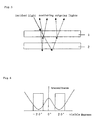
- the reflective polarizer 2 transmits only the P wave of the incident light as shown in Fig. 3, and reflects the S wave, and further transmits the P wave of the light reflected by the reflection face of back light unit or the like and reflects the S wave. While repeating this action, the S wave is converted into P wave, and the S wave that has not been used hitherto can be utilized, and therefore the brightness is raised notably by the use of the reflective polarizer.
- the reflective polarizer 2 is available in laminate type and cholesteric liquid crystal type, and they are equal in effects.
- this reflective polarizer 2 in the liquid crystal display of cellular telephone, PDA or the like, it is required to secure brightness when reflecting. When adhering to raise the brightness in transmission too much, the brightness in reflection is lowered. It is the primary object of the present invention to provide an optical film realizing a bright and visible excellent image in both transmission and reflection states in the liquid crystal display of cellular telephone, PDA or the like. Therefore the optical characteristic of the optical film of the present invention is explained more specifically. In this explanation, the light characteristic in two states of transmission and reflection is described while referring also to Fig. 4 and showing the optical characteristic of each film.
- Fig. 4 is a brightness distribution of light from the back light outgoing through the reflective polarizer 2.
- the BEF light collecting sheet
- the light from the back light is collected, and enters the reflective polarizer.
- the incident light is further enhanced in brightness by P/S conversion shown in Fig. 3, and gets into the light scattering film 1.
- the transmission light from the light scattering film 1 shows the viewing angle dependence as shown in Fig. 4, and when the transmission light transmits more near the normal line and the transmittance becomes smaller at the wider angle side, and the transmission becomes minimum around ⁇ 20 degrees to the normal line, that is, the scattering reaches the maximum.
- the BEF is not particularly required in the back light unit, and collecting of light is not always needed.
- the light intense region in the center is the region near the normal direction of the light scattering film (the region of relatively high transmittance), and the light transmits without having effects of scatter practically same as described above, and the light around ⁇ 20 degrees to the normal line is scattered and diffuses in the periphery.
- the light scattering film 1 used herein is small in the scattering angle (when defined by the half width of scattering light in Gaussian distribution, the half width of the light scattering film of the present invention is 10 degrees to 30 degrees), and the scattered light is focused in a direction closer to the normal direction of the film.
- the optical film of the present invention in transmission realizes an ideal display state high in the brightness in the normal direction and suppressed moderately in glare.
- Fig. 6 is a diagram showing a maximum scattering region of visible angle given by the optical scattering film of the optical film of the present invention.
- the range of 10 degrees to 15 degrees around the visible angles of +20 degrees and - 20 degrees is the angle contributing most to the scatter. That is, the light inclined by 20 degrees from the normal direction of the optical film surface is scattered most intensely, which contributes to the brightness in reflection.
- the light source is usually considered to be positioned in a direction deviated by about 20 degrees from the front side, and it is considered ideal to set the maximum scatter angle at ⁇ 20 degrees to the normal direction of the light scattering film. Therefore, the scattering maximum angle of the optical film of the present invention is considered to be closest to the ideal point.
- Fig. 5 is a schematic expression of propagation of light when the light enters at about 20 degrees from the normal direction.
- the light scattering film 1 of the present invention tends to scatter the incident light of about 20 degrees most efficiently and then collect the light in the front direction by focusing.
- the optical film of the present invention has the properties of transmitting the light efficiently and displaying the image clearly without lowering the brightness at the time of transmission, and collecting the peripheral light, especially the light from the light source at the front side efficiently in the normal direction of the film, that is, in the viewing angle direction at the time of reflection, and is hence an optical film most appropriate in a transflection type liquid crystal display device to be used in cellular telephone, PDA or the like.
- a DBEF of 3M Co. was used, and an acrylic adhesive 3 was coated on this DBEF in a thickness of 25 ⁇ m.
- An MFI 50A1000 of Microsharp Co. was adhered thereon as a light scattering film 1, and an optical film having a structure as shown in Fig. 7 was laminated.
- This film was disposed on a back light unit 4 , and the brightness was measured by a photodetector 5.
- measurement of the brightness in the film normal direction is being conducted by measuring the amount of outgoing light 6 in the normal direction of the film with photodetector 5.
- Example 1 an SK80 of Sumitomo Chemical Industry Co. which is a light scattering adhesive dispersing transparent fine particles different in refractive index in a conventional acrylic adhesive was disposed on the back light unit 4, and the brightness was measured by the photodetector 5.
- SK80 of Sumitomo Chemical Industry Co. which is a light scattering adhesive dispersing transparent fine particles different in refractive index in a conventional acrylic adhesive was disposed on the back light unit 4, and the brightness was measured by the photodetector 5.
- Example 1 The brightness was compared between Example 1 and Comparative Example, and it was known that the brightness of the optical film in Example 1 was higher by 30% to 50% as compared with that of the film in the Comparative Example.
- Example 2 An optical film was laminated in the same manner as in Example 1 except that a PCF400 of Nitto Denko Co. was used as the reflective polarizer 2, and the film was disposed on the back light unit 4 , and the brightness was measured in the same manner as in Example 1.
- a PCF400 of Nitto Denko Co. was used as the reflective polarizer 2
- the film was disposed on the back light unit 4 , and the brightness was measured in the same manner as in Example 1.
- the brightness of the optical film in Example 2 was higher by 30% to 50% as compared with that of the film in the Comparative Example.
- Example 2 An optical film was laminated in the same manner as in Example 1 except that a Transmax of Merck Co. was used as the reflective polarizer 2, and the film was disposed on the back light unit 4, and the brightness was measured in the same manner as in Example 1.
- a Transmax of Merck Co. was used as the reflective polarizer 2
- the film was disposed on the back light unit 4, and the brightness was measured in the same manner as in Example 1.
- the brightness of the optical film in Example 3 was higher by 30% to 50% as compared with that of the film in the comparative example.
Landscapes
- Physics & Mathematics (AREA)
- General Physics & Mathematics (AREA)
- Optics & Photonics (AREA)
- Nonlinear Science (AREA)
- Chemical & Material Sciences (AREA)
- Crystallography & Structural Chemistry (AREA)
- Mathematical Physics (AREA)
- Optical Elements Other Than Lenses (AREA)
- Liquid Crystal (AREA)
- Polarising Elements (AREA)
- Surface Treatment Of Optical Elements (AREA)
Abstract
Description
Claims (8)
- An optical film which is a layered product of a light scattering film that scatters and transmits light and is constituted by at least two phases or more having different refractive indexes each other, and a reflective polarizer by which light is selectively P/S converted.
- The optical film according to Claim 1, wherein at least one of the phases which has a greater refractive index in the light scattering film has pillar structures extending in the thickness direction of the film, and the transmittance of the film in the normal direction of the film is not less than 4 %.
- The optical film according to Claim 1 or 2, wherein axis lines of the pillar structures extending in the thickness direction of the light scattering film are in parallel with each other and the direction of the axis lines thereof are orientated in the normal direction to the film.
- The optical film according to Claim 1 or 2, wherein axis lines of the pillar structures extending in the thickness direction of the light scattering film are in parallel with each other and the direction of the axis lines are inclined with respect to the normal direction to the film.
- The optical film according to any one of claims 1 to 4, wherein difference in refractive indexes between at least two phases or more having different refractive indexes of the light scattering film is in a range of 0.005 to 0.1.
- The optical film according to any one of claims 1 to 5, wherein said light scattering film is made from a polymer material having a radiation sensitive property.
- The optical film according to any one of claims 1 to 6, wherein said reflective polarizer is of a lamination type.
- The optical film according to any one of claims 1 to 6, wherein said reflective polarizer is a film making use of selective reflection characteristic of cholesteric liquid crystal.
Applications Claiming Priority (3)
| Application Number | Priority Date | Filing Date | Title |
|---|---|---|---|
| JP2001123389 | 2001-04-20 | ||
| JP2001123389A JP2002318311A (en) | 2001-04-20 | 2001-04-20 | Optical film with controlled scattering and transmission characteristics |
| PCT/JP2002/003760 WO2002086562A1 (en) | 2001-04-20 | 2002-04-16 | Optical film having controlled scattering/transmitting characteristics |
Publications (2)
| Publication Number | Publication Date |
|---|---|
| EP1385025A1 true EP1385025A1 (en) | 2004-01-28 |
| EP1385025A4 EP1385025A4 (en) | 2005-06-22 |
Family
ID=18972952
Family Applications (1)
| Application Number | Title | Priority Date | Filing Date |
|---|---|---|---|
| EP02717166A Ceased EP1385025A4 (en) | 2001-04-20 | 2002-04-16 | OPTICAL FILM WITH REGULATED DIFFUSION / TRANSMISSION FEATURES |
Country Status (8)
| Country | Link |
|---|---|
| US (1) | US7154672B2 (en) |
| EP (1) | EP1385025A4 (en) |
| JP (1) | JP2002318311A (en) |
| KR (1) | KR100824226B1 (en) |
| CN (1) | CN1265217C (en) |
| MY (1) | MY137793A (en) |
| TW (1) | TW559675B (en) |
| WO (1) | WO2002086562A1 (en) |
Cited By (1)
| Publication number | Priority date | Publication date | Assignee | Title |
|---|---|---|---|---|
| EP1677047A4 (en) * | 2003-07-28 | 2007-03-28 | Tomoegawa Co Ltd | SURFACE LIGHT SOURCE |
Families Citing this family (14)
| Publication number | Priority date | Publication date | Assignee | Title |
|---|---|---|---|---|
| JP4885380B2 (en) * | 2001-04-20 | 2012-02-29 | セイコーインスツル株式会社 | Liquid crystal display |
| WO2005088357A1 (en) * | 2004-03-16 | 2005-09-22 | Tomoegawa Co., Ltd. | Anisotropic diffusing medium and production method therefor |
| US7572490B2 (en) | 2004-04-27 | 2009-08-11 | Samsung Electronics Co., Ltd. | Brightness enhancement film for liquid crystal display and manufacturing method thereof |
| JP4135940B2 (en) * | 2004-10-20 | 2008-08-20 | 株式会社巴川製紙所 | Anisotropic diffusion media |
| KR100676886B1 (en) | 2005-02-24 | 2007-02-05 | 주식회사 엘지에스 | Reflective polarizing film and display device having same |
| JP5226289B2 (en) * | 2007-12-19 | 2013-07-03 | 株式会社巴川製紙所 | Transflective film laminate, optical member using the same, and liquid crystal display device |
| US20100142055A1 (en) * | 2008-10-15 | 2010-06-10 | Nitto Denko Corporation | Optical element, directional diffusion film, and method of manufacturing optical element |
| JP5818719B2 (en) * | 2012-03-05 | 2015-11-18 | 株式会社ジャパンディスプレイ | Display device and anisotropic scatterer |
| JP2014142502A (en) * | 2013-01-24 | 2014-08-07 | Japan Display Inc | Reflection type liquid crystal display device and electronic device |
| CN103885219A (en) * | 2014-03-13 | 2014-06-25 | 明基材料有限公司 | Light switching module |
| TWI648577B (en) * | 2017-06-06 | 2019-01-21 | 凌巨科技股份有限公司 | Reflecting layer design method and display device thereof |
| CN107121838B (en) * | 2017-06-13 | 2020-06-05 | 明基材料有限公司 | Backlight module |
| EP3470892A3 (en) * | 2017-10-11 | 2019-07-17 | Agc Inc. | Transparent screen |
| JP7555856B2 (en) | 2021-03-05 | 2024-09-25 | Toppanホールディングス株式会社 | Optical member and liquid crystal display device |
Family Cites Families (21)
| Publication number | Priority date | Publication date | Assignee | Title |
|---|---|---|---|---|
| DE3789858T2 (en) * | 1986-12-18 | 1994-09-01 | Nippon Sheet Glass Co Ltd | Light control plates. |
| KR970009135B1 (en) * | 1987-06-01 | 1997-06-05 | 사이언티픽 어플라이드 리서어치(에스에이알) 피엘씨 | Display device using light transmitting screen and manufacturing method thereof |
| JP2717304B2 (en) * | 1989-04-20 | 1998-02-18 | 住友化学工業株式会社 | Manufacturing method of light control plate |
| EP0479490A3 (en) | 1990-10-02 | 1992-08-12 | Physical Optics Corporation | Volume holographic diffuser |
| JP3211381B2 (en) * | 1992-06-25 | 2001-09-25 | 住友化学工業株式会社 | Manufacturing method of light control plate |
| DE69420290T2 (en) * | 1993-06-15 | 1999-12-09 | Nashua Corp., Nashua | Process for the production of a mask with randomly distributed openings for the production of a diffusing screen |
| JPH0764069A (en) * | 1993-08-25 | 1995-03-10 | Sumitomo Chem Co Ltd | Liquid crystal display |
| EP0800658B1 (en) * | 1994-12-28 | 2000-05-03 | Nashua Corporation | Light diffusing material |
| JPH08297210A (en) * | 1995-04-26 | 1996-11-12 | Sumitomo Chem Co Ltd | Optical film and liquid crystal display |
| JP2002501624A (en) * | 1997-03-06 | 2002-01-15 | ナシュア コーポレイション | Display using polarization maintaining diffusion sheet |
| JP3480260B2 (en) * | 1997-09-01 | 2003-12-15 | セイコーエプソン株式会社 | Liquid crystal devices and electronic equipment |
| JP3760635B2 (en) * | 1998-08-21 | 2006-03-29 | セイコーエプソン株式会社 | Liquid crystal display device and electronic apparatus using the same |
| DE69919218T2 (en) * | 1998-12-31 | 2005-09-22 | Microsharp Corp. Ltd., Watchfield | STAGE-SHAPED STREUP SLATE |
| JP2000235181A (en) * | 1999-02-15 | 2000-08-29 | Seiko Epson Corp | Display device, electronic device using the same, and integrated optical film |
| KR100693680B1 (en) * | 1999-06-07 | 2007-03-09 | 닛토덴코 가부시키가이샤 | Diffusion Adhesive Layer, Optical Member, and Reflective Liquid Crystal Display Device |
| JP2001031774A (en) * | 1999-07-21 | 2001-02-06 | Daicel Chem Ind Ltd | Transmission type light scattering sheet and method for manufacturing the same |
| JP2001081292A (en) * | 1999-09-09 | 2001-03-27 | Toppan Printing Co Ltd | Composition for anisotropic light scattering film and anisotropic light scattering film |
| AU2515200A (en) * | 1999-09-20 | 2001-04-24 | 3M Innovative Properties Company | Optical films having at least one particle-containing layer |
| JP2001091708A (en) * | 1999-09-27 | 2001-04-06 | Keiwa Inc | Optical sheet and backlight unit using the same |
| WO2001096941A1 (en) * | 2000-06-12 | 2001-12-20 | Microsharp Corporation Limited | Screen with asymmetric light diffusing characteristic |
| AU2003270750A1 (en) * | 2002-09-20 | 2004-04-08 | Honeywell International, Inc. | High efficiency viewing screen |
-
2001
- 2001-04-20 JP JP2001123389A patent/JP2002318311A/en active Pending
-
2002
- 2002-04-15 TW TW091107586A patent/TW559675B/en not_active IP Right Cessation
- 2002-04-16 EP EP02717166A patent/EP1385025A4/en not_active Ceased
- 2002-04-16 MY MYPI20021395A patent/MY137793A/en unknown
- 2002-04-16 CN CNB028084063A patent/CN1265217C/en not_active Expired - Fee Related
- 2002-04-16 WO PCT/JP2002/003760 patent/WO2002086562A1/en not_active Ceased
- 2002-04-16 KR KR1020037013636A patent/KR100824226B1/en not_active Expired - Fee Related
-
2003
- 2003-10-17 US US10/688,541 patent/US7154672B2/en not_active Expired - Lifetime
Cited By (1)
| Publication number | Priority date | Publication date | Assignee | Title |
|---|---|---|---|---|
| EP1677047A4 (en) * | 2003-07-28 | 2007-03-28 | Tomoegawa Co Ltd | SURFACE LIGHT SOURCE |
Also Published As
| Publication number | Publication date |
|---|---|
| JP2002318311A (en) | 2002-10-31 |
| KR100824226B1 (en) | 2008-04-24 |
| TW559675B (en) | 2003-11-01 |
| CN1503917A (en) | 2004-06-09 |
| US20040085640A1 (en) | 2004-05-06 |
| CN1265217C (en) | 2006-07-19 |
| EP1385025A4 (en) | 2005-06-22 |
| WO2002086562A1 (en) | 2002-10-31 |
| US7154672B2 (en) | 2006-12-26 |
| MY137793A (en) | 2009-03-31 |
| KR20040000435A (en) | 2004-01-03 |
Similar Documents
| Publication | Publication Date | Title |
|---|---|---|
| TWI264563B (en) | Optical film with controlled light-scattering and light-transmission characteristics and liquid crystal display using the same | |
| JP4609962B2 (en) | Optical film | |
| JP4442836B2 (en) | Optical film | |
| KR100769779B1 (en) | Optical film and liquid-crystal display device | |
| KR100563159B1 (en) | Optical components with self-adhering diffuser | |
| US7154672B2 (en) | Optical film having controlled scattering/transmitting characteristics | |
| US6222598B1 (en) | Liquid crystal display | |
| JP4317006B2 (en) | Light diffusion film having controlled scattering characteristics, optical element using the same, and liquid crystal display device | |
| KR20020001594A (en) | Light pipe, plane light source unit and reflection type liquid-crystal display device | |
| JP2002148615A (en) | Optical film and reflective liquid crystal display | |
| KR100681103B1 (en) | Optical path polarizer | |
| JP4144829B2 (en) | Reflective and transmissive liquid crystal display device | |
| KR20010062553A (en) | Liquid-crystal display device | |
| KR20010051390A (en) | Liquid-crystal display device and light pipe | |
| JP2001228315A (en) | Reflector and liquid crystal display | |
| JP4103112B2 (en) | Condensing system and transmissive liquid crystal display device | |
| JP2000147429A (en) | Polarization plane light source device and liquid crystal display device | |
| JP2002006143A (en) | Light guide plate, surface light source device and reflection type liquid crystal display device | |
| JPH11306829A (en) | Light guide plate, surface light source device and reflection type liquid crystal display device | |
| JPH10333133A (en) | Reflection type liquid crystal display device | |
| CN111176033A (en) | Substrate with transparent electrode layer, dimming film and liquid crystal display device | |
| JP2003066236A (en) | Light guide plate, polarization plane light source device and reflection type liquid crystal display device | |
| JP3820623B2 (en) | Light guide plate and liquid crystal display device | |
| JP4548628B2 (en) | Optical film | |
| JP2000147488A (en) | Polarization plane light source device and liquid crystal display device |
Legal Events
| Date | Code | Title | Description |
|---|---|---|---|
| PUAI | Public reference made under article 153(3) epc to a published international application that has entered the european phase |
Free format text: ORIGINAL CODE: 0009012 |
|
| 17P | Request for examination filed |
Effective date: 20031120 |
|
| AK | Designated contracting states |
Kind code of ref document: A1 Designated state(s): AT BE CH CY DE DK ES FI FR GB GR IE IT LI LU MC NL PT SE TR |
|
| RAP1 | Party data changed (applicant data changed or rights of an application transferred) |
Owner name: CLARIANT FINANCE (BVI) LIMITED |
|
| RAP1 | Party data changed (applicant data changed or rights of an application transferred) |
Owner name: AZ ELECTRONIC MATERIALS USA CORP. |
|
| A4 | Supplementary search report drawn up and despatched |
Effective date: 20050509 |
|
| TPAC | Observations filed by third parties |
Free format text: ORIGINAL CODE: EPIDOSNTIPA |
|
| RAP1 | Party data changed (applicant data changed or rights of an application transferred) |
Owner name: TOMOEGAWA CO., LTD. |
|
| 17Q | First examination report despatched |
Effective date: 20050916 |
|
| TPAA | Information related to observations by third parties modified |
Free format text: ORIGINAL CODE: EPIDOSCTIPA |
|
| STAA | Information on the status of an ep patent application or granted ep patent |
Free format text: STATUS: THE APPLICATION HAS BEEN REFUSED |
|
| 18R | Application refused |
Effective date: 20081209 |