EP1383308A2 - Synchronizing video formats with dissimilar timing - Google Patents
Synchronizing video formats with dissimilar timing Download PDFInfo
- Publication number
- EP1383308A2 EP1383308A2 EP03254525A EP03254525A EP1383308A2 EP 1383308 A2 EP1383308 A2 EP 1383308A2 EP 03254525 A EP03254525 A EP 03254525A EP 03254525 A EP03254525 A EP 03254525A EP 1383308 A2 EP1383308 A2 EP 1383308A2
- Authority
- EP
- European Patent Office
- Prior art keywords
- signal
- video
- frequency
- phase
- locked loop
- Prior art date
- Legal status (The legal status is an assumption and is not a legal conclusion. Google has not performed a legal analysis and makes no representation as to the accuracy of the status listed.)
- Withdrawn
Links
Images


Classifications
-
- G—PHYSICS
- G09—EDUCATION; CRYPTOGRAPHY; DISPLAY; ADVERTISING; SEALS
- G09G—ARRANGEMENTS OR CIRCUITS FOR CONTROL OF INDICATING DEVICES USING STATIC MEANS TO PRESENT VARIABLE INFORMATION
- G09G5/00—Control arrangements or circuits for visual indicators common to cathode-ray tube indicators and other visual indicators
- G09G5/12—Synchronisation between the display unit and other units, e.g. other display units, video-disc players
-
- H—ELECTRICITY
- H04—ELECTRIC COMMUNICATION TECHNIQUE
- H04N—PICTORIAL COMMUNICATION, e.g. TELEVISION
- H04N21/00—Selective content distribution, e.g. interactive television or video on demand [VOD]
- H04N21/40—Client devices specifically adapted for the reception of or interaction with content, e.g. set-top-box [STB]; Operations thereof
- H04N21/43—Processing of content or additional data, e.g. demultiplexing additional data from a digital video stream; Elementary client operations, e.g. monitoring of home network or synchronising decoder's clock; Client middleware
- H04N21/4302—Content synchronisation processes, e.g. decoder synchronisation
- H04N21/4305—Synchronising client clock from received content stream, e.g. locking decoder clock with encoder clock, extraction of the PCR packets
-
- H—ELECTRICITY
- H04—ELECTRIC COMMUNICATION TECHNIQUE
- H04N—PICTORIAL COMMUNICATION, e.g. TELEVISION
- H04N21/00—Selective content distribution, e.g. interactive television or video on demand [VOD]
- H04N21/40—Client devices specifically adapted for the reception of or interaction with content, e.g. set-top-box [STB]; Operations thereof
- H04N21/43—Processing of content or additional data, e.g. demultiplexing additional data from a digital video stream; Elementary client operations, e.g. monitoring of home network or synchronising decoder's clock; Client middleware
- H04N21/4302—Content synchronisation processes, e.g. decoder synchronisation
- H04N21/4307—Synchronising the rendering of multiple content streams or additional data on devices, e.g. synchronisation of audio on a mobile phone with the video output on the TV screen
- H04N21/43072—Synchronising the rendering of multiple content streams or additional data on devices, e.g. synchronisation of audio on a mobile phone with the video output on the TV screen of multiple content streams on the same device
-
- H—ELECTRICITY
- H04—ELECTRIC COMMUNICATION TECHNIQUE
- H04N—PICTORIAL COMMUNICATION, e.g. TELEVISION
- H04N5/00—Details of television systems
- H04N5/04—Synchronising
- H04N5/06—Generation of synchronising signals
- H04N5/067—Arrangements or circuits at the transmitter end
- H04N5/073—Arrangements or circuits at the transmitter end for mutually locking plural sources of synchronising signals, e.g. studios or relay stations
-
- H—ELECTRICITY
- H04—ELECTRIC COMMUNICATION TECHNIQUE
- H04N—PICTORIAL COMMUNICATION, e.g. TELEVISION
- H04N5/00—Details of television systems
- H04N5/04—Synchronising
- H04N5/12—Devices in which the synchronising signals are only operative if a phase difference occurs between synchronising and synchronised scanning devices, e.g. flywheel synchronising
- H04N5/126—Devices in which the synchronising signals are only operative if a phase difference occurs between synchronising and synchronised scanning devices, e.g. flywheel synchronising whereby the synchronisation signal indirectly commands a frequency generator
-
- H—ELECTRICITY
- H04—ELECTRIC COMMUNICATION TECHNIQUE
- H04N—PICTORIAL COMMUNICATION, e.g. TELEVISION
- H04N5/00—Details of television systems
- H04N5/44—Receiver circuitry for the reception of television signals according to analogue transmission standards
- H04N5/46—Receiver circuitry for the reception of television signals according to analogue transmission standards for receiving on more than one standard at will
-
- H—ELECTRICITY
- H04—ELECTRIC COMMUNICATION TECHNIQUE
- H04N—PICTORIAL COMMUNICATION, e.g. TELEVISION
- H04N5/00—Details of television systems
- H04N5/74—Projection arrangements for image reproduction, e.g. using eidophor
Definitions
- the video source can be a computer graphics accelerator.
- synchronizing graphics accelerators is accomplished by means of asynchronous frame reset, where a Frame Reset signal from a first graphics accelerator, designated as a Master, is used to reset the video timing circuits of one or more second graphics accelerators, designated as Slaves.
- a Frame Reset signal from a first graphics accelerator, designated as a Master
- Slaves second graphics accelerators
- the video timing of the one or more Slaves is asynchronously reset at a set time in the Master's video timing.
- the Slaves upon receipt of the Frame Reset signal, reset their vertical counters at the next horizontal line boundary.
- the video timing circuitries of the Master and of the one or more Slaves operate independently, each deriving their respective timebase, from a local crystal oscillator, usually at 13.5MHz.
- the problem with the Framelock synchronization technique is a potential for frequency drift in the independent timebase between the Master and the one or more Slaves, caused by the independent operation of the local timebase crystals.
- the frequency drift can cause the Frame Reset signal to be received by the Slave at different times during successive frames, potentially on different video scanlines in successive frames.
- each of the crystals may have timing variations, or tolerances, which can cause a timebase to be slightly faster or slower then the other(s). These variations can result in dropped video lines if the Master resets a Slave whose video timing has not progressed to the same line as the Master.
- the dropped lines can cause problems in display devices connected to the slave machine.
- Most multisync monitors will blank their screens and attempt to configure their timing to a new video format, which occurs when the multisync monitor detects a change in the total number of lines per frame of input video.
- the Framelock synchronization technique may be insufficient to achieve frame synchronization required by many high-end visualization-simulation and scientific visualization applications.
- Genlock is a synchronization technique that solves the dropped line problem by effectively eliminating the independent timebases of the Master and of the one or more Slaves.
- the Master's video signals are used to generate clock signals in the one or more Slaves by using a phase-locked loop (PLL), whose operation is described below.
- Genlocking a technique whereby the Slave's pixel clock is generated by phase-locking to the video synchronization information of the Master, eliminates the need for the Slave's local 13.5MHz timebase. This prevents any drift arising from independent crystal oscillators.
- This lack of drift between video formats on the Master and on the one or more Slaves ensures that the one or more Slaves receive the Master Frame Reset signal at the same point on subsequent frame boundaries. In other words, video frames are perfectly synchronized using the Genlock technique.
- FIG 1 illustrates a conventional phase lock loop (PLL) 100, in which phase locking of two signals, an external signal 116 and a local signal 110, takes place.
- Phase lock loop 100 includes a phase difference detector 102, a loop filter 104, a clock generator 106, which may be a Voltage controlled Oscillator (VCO).
- VCO Voltage controlled Oscillator
- the PLL also includes a predivider 100 and a feedback frequency divider 108, which actually acts as a frequency multiplier.
- a PLL may also have a clock generator, such as a crystal (not shown).
- Phase difference detector 102 determines the phase difference between local signal 110 and an external signal 116.
- External signal 116 may be received from an external signal source. If the value of actual phase difference signal is equal to zero, local signal 110 is locked in phase with external signal. If the value of actual phase difference signal is not equal to zero, local signal 110 is not locked in phase with external signal, and the frequency of local signal 110 needs to be corrected in order to affect the phase of local signal 110 relative to external signal 116.
- Clock generator 108 which may be a voltage controlled oscillator (VCO), creates a local signal 110.
- VCO voltage controlled oscillator
- Genlock synchronization technique The problem with the Genlock synchronization technique is that the PLLs used for Genlocking typically require that the video formats of the Master and the one or more Slaves being synchronized are identical. Genlock is almost never an option for synchronizing video formats with the same frame rate and different resolution. This limitation of the Genlock technique is inconvenient when filming computer graphic displays, or when using display devices with dissimilar video timing formats that must be synchronized to prevent crawling bands on the displays. In addition, for operator training simulation, the out-the-window displays need to be synchronized with tactical and instrument displays.
- phase locked loop circuits may be used in tandem.
- a first PLL circuit may be connected to the first video format (Master) and generate an intermediate frequency.
- a second PLL circuit may use the intermediate frequency as the timebase for generating the pixel clock for the second video format (Slave).
- One or more Slaves may be connected to the generated pixel clock.
- the video synchronizing device may be a part of a graphics system, such as a graphics accelerator.
- the graphic system may include one or more filtering units.
- the one or more filtering units are operable to filter samples and produce pixels.
- Each one of the one or more filtering units may include one or more video synchronizing devices.
- the video synchronization device may be used to synchronize a local video signal and an external video signal.
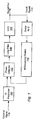
- Figure 2 illustrates a basic block diagram of a video synchronizing device, according to one embodiment.
- the video synchronizing device may be a part of a graphics system, such as a graphics accelerator.
- the graphic system may include one or more filtering units.
- the one or more filtering units are operable to filter samples and produce pixels.
- Each one of the one or more filtering units may include one or more video synchronizing devices.
- the video synchronization device may be used to synchronize a local video signal and an external video signal.
- the video synchronizing device 200 is operable to synchronize a first video signal 250 having a first video format with a second video signal having a second video format.
- the first video format may be referred to herein as a Master video signal
- the second video format may be referred to herein as a Slave video signal. Both the first and the second video signals should have the same frame rate.
- the video formats of each of the first and the second video signals may be dissimilar, meaning the video formats can have different resolution.
- the video synchronizing device 200 may include a genlock signal input terminal also referred to herein as the synchronization stripper device 210, operable to receive a genlock signal from the first video signal 250, and propagate a derived, or stripped, signal of a first frequency.
- the stripped signal can form a stripped genlock signal and may, for example, include a Composite Synchronization signal CSync 260 and a Horizontal Synchronization signal HSync 270 for the first video signal 250.
- a synchronization stripper device 210 is operable to receive and operate on the at least a part of the first video signal 250, where the first video signal can have a very wide frequency range, such as 15 kHz to 121 kHz.
- a Frame Reset signal from the first video signal 250 may be propagated to the video synchronizing device 200.
- the internal frequency divider N1 276 of the first phase-locked loop circuit 202 is not utilized, as the local timebase 300 is not connected through a multiplexer 240.
- the Hsync signal from the first video signal 250 is used as a timebase for the first PLL 202.
- the first phase-locked loop 202 may be operable to use an internal frequency multiplier M1 270 instead of an input from a Video Timing Generator.
- the video synchronizing device 200 may include a second phase-locked loop circuit 204 operable to receive the intermediate signal 260 and produce a final signal 264 of a final frequency.
- the second phase-locked loop circuit 204 may include a logic circuit 290 operable to operate on the intermediate signal 260 to produce an operated intermediate signal 262.
- the second phase-locked loop circuit 204 may be operable to divide the frequency of the intermediate signal 260 by a second division factor N2 to produce the operated intermediate signal 262.
- the N2 divider implemented by the logic circuit 290 may be operable to function analogously to an internal frequency divider 278 of the second phase-locked loop circuit 204.
- the internal frequency divider 278 of the second phase-locked loop circuit 204 is not utilized.
- a multiplexer 242 may select the operated intermediate signal 262 from the first PLL 202 as the timebase of the second PLL 204 instead of the local timebase 302.
- the second phase-locked loop circuit 204 may be further operable to multiply the frequency of the intermediate signal by a second multiplication factor M2 to produce the final signal 264 of a final frequency.
- the second phase-locked loop circuit 204 may couple to a video timing generator 280.
- the video timing generator may be operable to produce a frequency multiplier M2 used by the second phase-locked loop circuit 204.
- the video timing generator 280 may be operable to produce the frequency multiplier M2 while being synchronized with the second phase-locked circuit 204.
- a multiplexer 243 may select the frequency multiplier M2 generated by the VTG 280 instead of the internal frequency multiplier M2 272, which will not be used.
- the first PLL circuit 202 may be connected to the first video format (Master) and generate the intermediate frequency 360.
- the second PLL circuit 204 may use the intermediate frequency as the timebase for generating the pixel clock, or the final signal 264 for the second video format (Slave).
- One or more Slaves may be connected to the generated pixel clock.
- Figure 3 is a detailed block diagram of a Video Synchronizing Device, according to one embodiment.
- Figure 3 shows one embodiment of a detailed implementation of the video synchronizing device 200 of Figure 2.
- the tandem PLL arrangement allows dissimilar video formats to be synchronized. If the frame rates of the dissimilar video formats are the same, the Frame Reset signal can be used to achieve vertical synchronization once the pixel clock has been synchronized.
- VTG's 280, 280A, 280B, and 280C there may be a plurality of VTG's 280, 280A, 280B, and 280C.
- the N2 divider in the logic circuit 290 can be programmed to produce the Hsync signal produced by the Video Timing Generator (VTG) 280 for interlaced video formats. This signal may be passed to the one or more second PLL's 204A and 204B, which can lock and produce the pixel clock.
- VTG Video Timing Generator
- the N2 divider 292 in the logic circuit 290 may be able to be synchronously reset by the incoming Hsync signal, such that the Hsync signal produced by the N2 divider 292 has zero phase with the first video signal 250. This allows the one or more second PLL's 204A and 204B to lock with the Hsync signal from the VTG 280, with either Zero or Hperiod/2 phase with respect to the incoming video timing.
- the VTG Csync signals can be passed to the logic circuit 290 for a determination of synchronization phase. If the synchronization phase is Hperiod/2, the logic circuit 290 N2 divider can be skip clock pulses from the first PLL 202 until the horizontal phase of the VTG 280 is zero with respect to the incoming video timing from the first video signal 250.
- an ability to adjust VTG horizontal phase by means of the N2 divider 292 may be also under user control.
- System software can adjust the phase of the Hsync produced by the N2 divider 292 to include a selected horizontal phase with respect to the incoming Master video timing from the first video signal 250.
- interlaced, progressive, and/or and stereo video formats can be phase adjusted by programming the logic circuit 290 N2 divider to produce a pure Hsync signal, instead of 2xHsync for interlace formats.
- the Hsync signal can then be sent to the one or more second PLL's 204A and 204B.
- each PLL may contain a sub-pixel, Dynamic Phase Adjustment (DPA) 350, 352A, and 352B.
- the DPA clock output may be used on the first PLL 202.
- the first PLL 202 may have two PECL clock outputs 366 and 368, the first PECL output 366 containing the DPA function, and the second PECL 368 without.
- the DPA adjustment may be used for pixel clocks below 160MHz, and the first PECL output 366 should be used.
- sub-pixel phase adjustment is not usually necessary, and the non-DPA PECL clock output 368 should be used to ensure good duty-cycle on the PixClk. This is critical for PixClks above 200MHz.
- Both of these PECL clock outputs 366 and 368 may be propagated to the logic circuit 290, which may be operable to select one of these clocks.
- the VTG Frame Detector may implement vertical phase adjustments.
- the video synchronization device may have complete horizontal and subpixel genlock phase adjustment.
- the first PLL 202 may be programmed with an internal divide (M1 multiplier) of 157, producing a clock rate of 10.125MHz.
- the N2 divider in the logic circuit 290 may be programmed to a value of 3, producing an intermediate frequency of 3.375MHz. This is the Hsync input to the second PLL 204A and 204B, which should be between 8.0KHz and 10.0MHz.
- the feedback divider M2 of the second PLL 204A and 204B is 40, producing the desired frequency of 135.000MHz.
- the limits on feedback divider modulus for the PLL may be as follows, depending on the hardware implementation. 8 ⁇ M ⁇ 4103
- the internal VCO of the PLL may run at a rate between 100MHz and 500MHz. This may be easily accomplished by adjusting the post-scaler divider, if necessary.
- a post-scale divisor of 2 can be used, so that the VCO runs at 270MHz.
- a second PLL 204A and/or 204B may use a phase detector to make a correction in its VCO's frequency.
- Moderate values of M1, N1, M2, N2 should result in good PLL transfer gain.
- the feedback divider also referred to as the internal multiplier, M1 270 of the first PLL 202 should have a larger value than that of the second PLL 204 feedback divider (M2, which may be implemented by the VTG 280).
- M1 was programmed to 157, and M2 to 40. This allows the second PLL 204 to respond faster than the first PLL 202, essentially tracking the first PLL's 202 transients and deviations about its nominal frequency.
- each PLL may include a Phase/Frequency Detector and a corresponding Phase/Frequency Detector Gain register (PFDGain), which may control the closed-loop bandwidth of each PLL.
- the PFDGain value indicates how much current will be issued by the phase detector in response to a given phase error. The magnitude of this current controls the change in VCO control voltage in response to a phase or frequency error measured by the Phase/Frequency Detector. Intuitively, a smaller value of PFDGain will cause the PLL to take longer to eliminate a phase or frequency difference at the inputs to the PFD.
- a too-large PFDGain value may cause the loop to over-correct for such a phase difference, resulting in ringing in the loop response.
- the value programmed into the PFDGain register of the second PLL 204 should be equal to or greater than the value programmed into the PFDGain register of the first PLL 202. This may result in a faster response by the second PLL 204 than the first PLL 202, in effect allowing the first PLL 202 to dominate the overall loop characteristics.
- more than two video synchronizing devices can be genlocked together.
- Such daisy-chain effectively puts the PLLs of these systems in tandem, which usually increases clock jitter down the daisy-chain.
- a distribution amplifier may be used to obtain the needed copies of the Master's genlock signal.
- a BNC T connector may be used to connect the genlock inputs of the Slaves to the Master's video signal.
- a first PLL circuit may be connected to the first video format (Master) and generate an intermediate frequency.
- a second PLL circuit may use the intermediate frequency as the timebase for generating the pixel clock for the second video format (Slave).
- One or more Slaves may be connected to the generated pixel clock.
- the video synchronizing device may be a part of a graphics system, such as a graphics accelerator.
- a method to synchronize two video signals wherein a first video signal has a first video format and a second video signal has a second video format, both video signals have the same frame rate, the method comprising: receiving a genlock signal from the first video signal; stripping the genlock signal in order to propagate a stripped genlock signal of a first frequency; a first phase-locked loop circuit receiving at least a part of the stripped genlock signal and producing an intermediate signal of an intermediate frequency; and a second phase-locked loop circuit receiving the operated intermediate signal and producing a final signal of a final frequency; wherein the first phase-locked loop and the second phase-locked loop are coupled together.
- a system for synchronizing two video signals of different formats wherein a first video signal has a first video format, wherein a second video signal has a second video format, wherein both video signals have the same frame rate
- the system comprising: a genlock signal input terminal operable to receive a genlock signal from the first video signal, and propagate a Hsync signal of a first frequency; a first phase-locked loop circuit operable to receive the Hsync signal and produce an intermediate signal of an intermediate frequency; and a second phase-locked loop circuit operable to receive the operated intermediate signal and produce a final signal of a final frequency; wherein the final signal is operable to synchronize the second video signal to the first video signal.
- a graphics system comprising: one or more filtering units, wherein the one or more filtering units are operable to filter samples and thereby produce pixels, wherein each one of the one or more filtering units comprises one or more video synchronizing devices, wherein the one or more video synchronizing devices are operable to synchronize two video signals with different formats; wherein each one of one or more video synchronizing devices is operable to synchronize a first video signal having a first video format and a second video signal having a second video format, both video signals having the same frame rate, the video synchronizing device comprising: a genlock signal input terminal operable to receive a genlock signal from the first video signal, and propagate a stripped genlock signal of a first frequency; a first phase-locked loop circuit operable to receive at least a part of the stripped genlock signal and produce an intermediate signal of an intermediate frequency; a second phase-locked loop circuit operable to receive the operated intermediate signal and produce a final signal of a final frequency.
Landscapes
- Engineering & Computer Science (AREA)
- Multimedia (AREA)
- Signal Processing (AREA)
- Physics & Mathematics (AREA)
- Computer Hardware Design (AREA)
- General Physics & Mathematics (AREA)
- Theoretical Computer Science (AREA)
- Control Of Indicators Other Than Cathode Ray Tubes (AREA)
- Controls And Circuits For Display Device (AREA)
- Synchronizing For Television (AREA)
Abstract
Description
| Video Format | Subscript | M | N | PixClksPerHperiod | PixClk Frequency | Hrate |
| 1280x800 @ 76Hz | 1 | 45 | 6 | 1570 | 101.250MHz | 64.4904KHz |
| 1280x1024 @ | 2 | 40 | 4 | 1664 | 135.000MHz | 81.1298KHz |
Claims (22)
- A video synchronizing device, wherein the video synchronizing device is operable to synchronize a first video signal having a first video format and a second video signal having a second video format, both video signals having the same frame rate, the video synchronizing device comprising:a genlock signal input terminal (210) operable to receive a genlock signal from the first video signal, and propagate a stripped genlock signal of a first frequency;a first phase-locked loop circuit (202) operable to receive at least a part of the stripped genlock signal and produce an intermediate signal of an intermediate frequency;a second phase-locked loop circuit (204) operable to receive the intermediate signal and produce a final signal of a final frequency.
- The video synchronizing device of claim 1,
wherein the second phase-locked loop circuit comprises a logic circuit operable to operate on the intermediate signal to produce an operated intermediate signal; - The video synchronizing device of any one of the preceding claims,
wherein the first phase-locked loop circuit is operable to divide the frequency of the at least a part of the stripped genlock signal by a first division factor to produce the intermediate signal of the intermediate frequency. - The video synchronizing device of any one of the preceding claims,
wherein the second phase-locked loop circuit is operable to divide the frequency of the intermediate signal by a second division factor; and
wherein the second phase-locked loop circuit is further operable to multiply the frequency of the intermediate signal by a second multiplication factor to produce the final signal of the final frequency. - The video synchronizing device of claim 4,
wherein the second phase-locked loop circuit comprises a logic circuit;
wherein the logic circuit is operable to divide the frequency of the intermediate signal by a second division factor prior to passing the divided intermediate signal to a remainder of the second phase-locked loop circuit. - The video synchronizing device of claim 5,
wherein the logic circuit is operable to function analogously to an internal frequency divider of the second phase-locked loop circuit. - The video synchronizing device of claim 6,
wherein an internal frequency divider of the second phase-locked loop circuit is not utilized. - The video synchronizing device of any one of the preceding claims,
wherein an internal frequency divider of the first phase-locked loop circuit is not utilized. - The video synchronizing device of any one of the preceding claims,
wherein the first phase-locked loop circuit is operable to use an internal frequency multiplier. - The video synchronizing device of any one of the preceding claims, further comprising a video timing generator;
wherein the video timing generator is operable to produce a frequency multiplier used by the second phase-locked loop circuit. - The video synchronizing device of claim 10,
wherein the video timing generator is operable to produce the frequency multiplier while being synchronized with the second phase-locked loop circuit. - The video synchronizing device of any one of the preceding claims,
wherein the final frequency of the final signal is substantially equal to:
wherein M1 is the value of an internal frequency multiplier of the first phase-locked loop circuit;
wherein M2 is the value of an internal frequency multiplier of the second phase-locked loop circuit;
wherein N2 is the value of an internal frequency divider of the second phase-locked loop circuit, and
wherein FFinal is the final frequency of the final signal. - The video synchronizing device of any one of the preceding claims, further comprising:a frame reset input terminal operable to receive a frame reset signal from the first video signal.
- The video synchronizing device of any one of the preceding claims,
wherein the final signal of the final frequency is operable to be used as a pixel clock for the second video signal. - The video synchronizing device of any one of the preceding claims,
wherein the stripped genlock signal of a first frequency comprises a composite synchronization signal CSync and a horizontal synchronization signal HSync. - The video synchronizing device of any one of claims 1 to 14,
wherein the at least a part of the stripped genlock signal comprises an Hsync signal of the first frequency. - The video synchronizing device of any one of the preceding claims,
wherein the final signal is operable to synchronize the second video signal to the first video signal. - A graphics system, comprising:one or more filtering units, wherein the one or more filtering units are operable to filter samples and thereby produce pixels, wherein each one of the one or more filtering units comprises one or more video synchronizing devices, according to any one of the preceding claims.
- A method to synchronize two video signals, wherein a first video signal has a first video format and a second video signal has a second video format, both video signals have the same frame rate, the method comprising:wherein the first phase-locked loop and the second phase-locked loop are coupled together.receiving a genlock signal from the first video signalstripping (210) the genlock signal in order to propagate a stripped genlock signal of a first frequency;a first phase-locked loop circuit (202) receiving at least a part of the stripped genlock signal and producing an intermediate signal of an intermediate frequency; anda second phase-locked loop circuit (204) receiving the operated intermediate signal and producing a final signal of a final frequency;
- The method of claim 19,
wherein the final frequency of the final signal is substantially equal to:
wherein M1 is the value of an internal frequency multiplier of the first phase-locked loop circuit;
wherein M2 is the value of an internal frequency multiplier of the second phase-locked loop circuit;
wherein N2 is the value of an internal frequency divider of the second phase-locked loop circuit, and
wherein FFinal is the final frequency of the final signal. - The method of claim 19 or claim 20,
wherein the final signal of final frequency is operable to be used as a pixel clock for the second video signal. - The method of any one of claims 19 to 21, further comprising a video timing generator;
wherein the video timing generator is operable to produce a frequency multiplier used by the second phase-locked loop circuit;
wherein the video timing generator is operable to produce the frequency multiplier while being synchronized with the second phase-locked circuit.
Applications Claiming Priority (2)
| Application Number | Priority Date | Filing Date | Title |
|---|---|---|---|
| US200032 | 2002-07-19 | ||
| US10/200,032 US7071996B2 (en) | 2002-07-19 | 2002-07-19 | Synchronizing video formats with dissimilar timing |
Publications (2)
| Publication Number | Publication Date |
|---|---|
| EP1383308A2 true EP1383308A2 (en) | 2004-01-21 |
| EP1383308A3 EP1383308A3 (en) | 2007-05-16 |
Family
ID=29780244
Family Applications (1)
| Application Number | Title | Priority Date | Filing Date |
|---|---|---|---|
| EP03254525A Withdrawn EP1383308A3 (en) | 2002-07-19 | 2003-07-18 | Synchronizing video formats with dissimilar timing |
Country Status (2)
| Country | Link |
|---|---|
| US (1) | US7071996B2 (en) |
| EP (1) | EP1383308A3 (en) |
Families Citing this family (15)
| Publication number | Priority date | Publication date | Assignee | Title |
|---|---|---|---|---|
| KR100580177B1 (en) * | 2003-09-22 | 2006-05-15 | 삼성전자주식회사 | Apparatus and decoder for display synchronization signal generation in digital broadcasting reception system and method thereof |
| US7425962B2 (en) * | 2004-07-27 | 2008-09-16 | Hewlett-Packard Development Company, L.P. | Systems and methods for generating a composite video signal from a plurality of independent video signals |
| US7548233B1 (en) * | 2004-09-10 | 2009-06-16 | Kolorific, Inc. | Method and system for image scaling output timing calculation and remapping |
| US8624895B2 (en) * | 2005-01-20 | 2014-01-07 | Production Resource Group, Llc | Controls for digital lighting |
| JP4572144B2 (en) * | 2005-07-06 | 2010-10-27 | Necディスプレイソリューションズ株式会社 | Display panel driving apparatus and display panel driving method |
| TWI292893B (en) * | 2005-10-05 | 2008-01-21 | Myson Century Inc | Method for prevention of distorted sub-picture display on flat panel display |
| FR2898453A1 (en) * | 2006-03-13 | 2007-09-14 | Thomson Licensing Sas | TRANSMISSION OF A GENLOCK SIGNAL OVER AN IP NETWORK |
| EP2153663B1 (en) * | 2007-06-12 | 2012-12-26 | Thomson Licensing | Automatic compensation of a delay of a synchronization signal in a packet switching network |
| US8407750B2 (en) * | 2007-07-11 | 2013-03-26 | Hewlett-Packard Development Company, L.P. | Enabling users of peer to peer clients to socially interact while viewing videos |
| US8707382B2 (en) * | 2008-02-13 | 2014-04-22 | At&T Intellectual Property I, L.P. | Synchronizing presentations of multimedia programs |
| US8059200B2 (en) * | 2008-04-14 | 2011-11-15 | National Semiconductor Corporation | Video clock generator for multiple video formats |
| US9122443B1 (en) | 2008-05-01 | 2015-09-01 | Rockwell Collins, Inc. | System and method for synchronizing multiple video streams |
| US8446527B2 (en) * | 2009-07-21 | 2013-05-21 | Qualcomm Incorporated | System of programmable time intervals used for video signal synchronization |
| US8368436B1 (en) * | 2010-10-29 | 2013-02-05 | Maxim Integrated, Inc. | Programmable frequency synthesizer with I/Q outputs |
| JP2016163311A (en) * | 2015-03-05 | 2016-09-05 | ソニー株式会社 | Video processing apparatus, video processing system, and video processing method |
Family Cites Families (16)
| Publication number | Priority date | Publication date | Assignee | Title |
|---|---|---|---|---|
| US5051817A (en) * | 1988-11-18 | 1991-09-24 | Rohm Co., Ltd. | Superimposing system |
| US5072195A (en) * | 1990-04-05 | 1991-12-10 | Gazelle Microcircuits, Inc. | Phase-locked loop with clamped voltage-controlled oscillator |
| US5541666A (en) * | 1994-07-06 | 1996-07-30 | General Instrument | Method and apparatus for overlaying digitally generated graphics over an analog video signal |
| JPH08223071A (en) * | 1995-02-08 | 1996-08-30 | Sony Corp | Transmitter and transceiver |
| US6310922B1 (en) * | 1995-12-12 | 2001-10-30 | Thomson Consumer Electronics, Inc. | Method and apparatus for generating variable rate synchronization signals |
| EP0794525B1 (en) * | 1996-03-06 | 2003-07-23 | Matsushita Electric Industrial Co., Ltd. | Pixel conversion apparatus |
| JPH10304400A (en) * | 1997-04-30 | 1998-11-13 | Sony Corp | Signal processing circuit |
| JP2000092409A (en) * | 1998-09-10 | 2000-03-31 | Sony Corp | Video display device |
| JP2000165905A (en) * | 1998-11-27 | 2000-06-16 | Mitsubishi Electric Corp | Clock generation circuit |
| US6385267B1 (en) * | 1998-12-22 | 2002-05-07 | Microsoft Corporation | System and method for locking disparate video formats |
| US6218876B1 (en) * | 1999-01-08 | 2001-04-17 | Altera Corporation | Phase-locked loop circuitry for programmable logic devices |
| US6417861B1 (en) * | 1999-02-17 | 2002-07-09 | Sun Microsystems, Inc. | Graphics system with programmable sample positions |
| US6989835B2 (en) * | 2000-06-28 | 2006-01-24 | Sun Microsystems, Inc. | Flexible video architecture for generating video streams |
| US6316974B1 (en) * | 2000-08-26 | 2001-11-13 | Rgb Systems, Inc. | Method and apparatus for vertically locking input and output signals |
| JP3781959B2 (en) * | 2000-09-29 | 2006-06-07 | Necディスプレイソリューションズ株式会社 | Image display device |
| JP2002252559A (en) * | 2001-02-23 | 2002-09-06 | Rohm Co Ltd | Reference clock generation system |
-
2002
- 2002-07-19 US US10/200,032 patent/US7071996B2/en not_active Expired - Lifetime
-
2003
- 2003-07-18 EP EP03254525A patent/EP1383308A3/en not_active Withdrawn
Also Published As
| Publication number | Publication date |
|---|---|
| US7071996B2 (en) | 2006-07-04 |
| US20040012578A1 (en) | 2004-01-22 |
| EP1383308A3 (en) | 2007-05-16 |
Similar Documents
| Publication | Publication Date | Title |
|---|---|---|
| EP1383308A2 (en) | Synchronizing video formats with dissimilar timing | |
| US6275553B1 (en) | Digital PLL circuit and clock generation method | |
| US8736515B2 (en) | Graphics card, multi-screen display system and synchronous display method | |
| US6285402B1 (en) | Device and method for converting scanning | |
| GB2415852A (en) | Synchronising a plurality of graphics cards | |
| JP2011150373A (en) | Display panel control circuit and display panel control method | |
| US20040012577A1 (en) | Synthesizing a pixel clock with extremely close channel spacing | |
| CN100527785C (en) | Display synchronization signal generation apparatus in digital broadcast receiver and decoder | |
| EP0859470B1 (en) | Synchronizing signal processing unit | |
| US6844785B2 (en) | Phase-lock loop for preventing frequency drift and jitter and method thereof | |
| CN101271679B (en) | Image data processing apparatus | |
| KR20080099197A (en) | Dot Clock Generation Circuit, Semiconductor Device, and Dot Clock Generation Method | |
| EP0662680A1 (en) | Apparatus and method for setting up a display monitor | |
| JP4449102B2 (en) | Image display device | |
| US5534939A (en) | Digital video clock generation system | |
| EP0966153A1 (en) | Video signal synchronizing apparatus | |
| KR100266164B1 (en) | Method for emboding sync of divided picture and apparatus thereof | |
| CN112218002B (en) | Video stitching processor, display system and video stitching processing method | |
| JP3638443B2 (en) | Television receiver for digital broadcasting | |
| JP2755324B2 (en) | Blanking circuit | |
| JP3353372B2 (en) | Liquid crystal display | |
| JPH10319933A (en) | Dot clock generation circuit | |
| JPH07336211A (en) | Clock signal generation circuit | |
| JP2878313B2 (en) | Clock generation circuit for video signal digitizing | |
| JPH04192971A (en) | Blanking pulse preparing circuit |
Legal Events
| Date | Code | Title | Description |
|---|---|---|---|
| PUAI | Public reference made under article 153(3) epc to a published international application that has entered the european phase |
Free format text: ORIGINAL CODE: 0009012 |
|
| AK | Designated contracting states |
Kind code of ref document: A2 Designated state(s): AT BE BG CH CY CZ DE DK EE ES FI FR GB GR HU IE IT LI LU MC NL PT RO SE SI SK TR |
|
| AX | Request for extension of the european patent |
Extension state: AL LT LV MK |
|
| PUAL | Search report despatched |
Free format text: ORIGINAL CODE: 0009013 |
|
| AK | Designated contracting states |
Kind code of ref document: A3 Designated state(s): AT BE BG CH CY CZ DE DK EE ES FI FR GB GR HU IE IT LI LU MC NL PT RO SE SI SK TR |
|
| AX | Request for extension of the european patent |
Extension state: AL LT LV MK |
|
| AKX | Designation fees paid | ||
| REG | Reference to a national code |
Ref country code: DE Ref legal event code: 8566 |
|
| STAA | Information on the status of an ep patent application or granted ep patent |
Free format text: STATUS: THE APPLICATION IS DEEMED TO BE WITHDRAWN |
|
| 18D | Application deemed to be withdrawn |
Effective date: 20071118 |