EP1382975A1 - Method of generating a test pattern for the simulation and/or test of the layout of an integrated circuit - Google Patents
Method of generating a test pattern for the simulation and/or test of the layout of an integrated circuit Download PDFInfo
- Publication number
- EP1382975A1 EP1382975A1 EP02090271A EP02090271A EP1382975A1 EP 1382975 A1 EP1382975 A1 EP 1382975A1 EP 02090271 A EP02090271 A EP 02090271A EP 02090271 A EP02090271 A EP 02090271A EP 1382975 A1 EP1382975 A1 EP 1382975A1
- Authority
- EP
- European Patent Office
- Prior art keywords
- test
- test patterns
- patterns
- input signals
- generating
- Prior art date
- Legal status (The legal status is an assumption and is not a legal conclusion. Google has not performed a legal analysis and makes no representation as to the accuracy of the status listed.)
- Granted
Links
Images


Classifications
-
- G—PHYSICS
- G01—MEASURING; TESTING
- G01R—MEASURING ELECTRIC VARIABLES; MEASURING MAGNETIC VARIABLES
- G01R31/00—Arrangements for testing electric properties; Arrangements for locating electric faults; Arrangements for electrical testing characterised by what is being tested not provided for elsewhere
- G01R31/28—Testing of electronic circuits, e.g. by signal tracer
- G01R31/317—Testing of digital circuits
- G01R31/3181—Functional testing
- G01R31/3183—Generation of test inputs, e.g. test vectors, patterns or sequences
- G01R31/318371—Methodologies therefor, e.g. algorithms, procedures
Definitions
- the dimensions of integrated circuit components are scaled down more and more.
- transistor dimensions are scaled down while lower power dissipation is achieved by scaling down the supply voltage.
- the power supply current is increasing, and hence, large current swings within a short period of time can cause considerable noise.
- one difficulty circuit designers face is the power delivery of very high performance circuits due to the severe switching noise.
- the circuit In order to verify the function of a newly designed integrated circuit, the circuit is first simulated and then tested. During simulation, multiple input signals are applied to the inputs of the circuit, and the output signals of the circuit calculated. The input signals are referred to as test patterns. If the output signals do not sufficiently approximate preset target signals, the circuit is redesigned and resimulated.
- ATE Automatic Test Equipment
- the ATE also applies a test pattern to the circuit.
- the test pattern for the ATE has to be input manually by a user. Generally, the same test pattern that has been used for simulation is also used for testing. If the output signals generated by the circuit in response to the test pattern of the ATE deviate from preset target signals, the circuit is redesigned, resimulated and retested.
- the design of an integrated circuit is simulated by applying randomly generated input signal vectors to the inputs of the circuit. For each input vector pair, the simulated peak switching current is determined.
- the worst case input vector pairs feed, as initial population, a genetic algorithm.
- the genetic algorithm is designed to single out the near optimal input pattern(s) that induce the steepest maximum switching current spike and, therefore, the worst case switching noise.
- the worst case input patterns are then used in HSPICE simulation of the circuits to extract the exact current waveform.
- the present invention aims to address this problem.
- a method of generating a set of test patterns for the simulation and/or test of the layout of an integrated circuit comprising the steps of:
- the method employs a genetic algorithm (optimization method) to optimize a set of random patterns based on measurements using an ATE. Thereby, a set of worst case noise patterns can be selected automatically.
- a genetic algorithm optimization method
- the selected set of worst case noise patterns can be used to re-simulate the layout of the integrated circuit for detail design analysis or improvement.
- This approach is more efficient and faster than any pure random-based method employing a non-optimal random pattern generation or simulation approach.
- a genetic algorithm can be equally employed to detect a set of potential worst case test conditions in respect of input signals supplied to an integrated circuit (e.g. power supply).
- the parameters of such input signals are referred to as AC/DC parameters.
- a method of generating a set of input signals for the simulation and/or test of the layout of an integrated circuit comprising the steps of:
- a set of worst case test conditions due to resulting high power supply noise can be detected without having to manually and/or randomly select parameters of input signals.
- This method may also be implemented using existing ATE systems.
- the input signals obtained as a result of this method may subsequently be re-simulated.
- the method of approximating a worst case set of test pattern is performed together with the method of approximating a set of worst case input signals parameters. This way, an overall worst case condition of operation of the integrated circuit can be approximated.
- Genetic algorithms are based on the principles of natural selection.
- genetic algorithms are stochastic search methods which simulate natural biological evolution.
- the algorithms operate on the basis of a population of potential solutions and, applying the principle of "survival of the fittest" to these potential solutions, produce a better approximation of a target solution in each iteration of the algorithm.
- the approximations of each generations are created by the process of selecting individuals according to their level of "fitness" in the problem domain.
- the selected individuals are bred with one another using operators borrowed from natural genetics. This process leads to the evolution of populations of individuals that are better suited for their environment than the individuals from which they were created, just as in natural adaptation.
- genetic algorithms model natural processes such as selection, cross over, recombination and mutation.
- Figure 1 shows a method for detecting the worst case current consumption/peak current pattern (RSMA) based on a genetic algorithm. This method operates on the basis of populations of individual patterns instead of a single pattern solution. In this way, the search for better approximations can be performed in a parallel manner. Therefore, this method is more efficient than single pattern searching processes using dynamic random algorithm methods.
- RSMA worst case current consumption/peak current pattern
- Genetic algorithms may be employed for the simulation of an integrated circuit design in order to solve the worst case pattern search problem.
- the efficiency of genetic searching procedures is largely dependent on the number of pattern populations and the number of test patterns in each pattern population.
- the simulation-based approach forms a limitation if genetic algorithms are to be employed.
- the full pattern combination domain increases proportionally to the complexity of VLSI or ULSI designs. Therefore, a subset of 200 pattern populations is only a very small subset of the full pattern combination domain.
- the basic concept of tournament selection is employed. That is, only the best individual pattern from the existing population is selected as a parent. This process is repeated until a pre-defined percentage of best patterns has been selected: wherein B is the pre-defined percentage of the best pattern group.
- the sorting function first re-arranges the test patterns from minimum to maximum according to their fitness values. Subsequently, the parent selection is generated in random sequence based on the new sub-optimal fitness range N, which is calculated using B. Parents (selected patterns) are combined using cross over (4), re-combined (5) and mutated (6) in order to produce offspring: where C is the test pattern content which is selected for cross over of two patterns.
- the mutation process helps to improve the optimization search process.
- Figure 2 illustrates an experimental plot of a dynamic genetic algorithm approach (100MHz, VDDP IO Pad eDRAM core).
- the experiment lasted considerably shorter than a simulation-based approach, and the current bound obtained through using the worst case pattern was higher compared to conventional dynamic random algorithm-based approaches.
- the maximum switching noise occuring during operation of an integrated circuit is directly related to the steepest maximum switching dynamic current spike.
- the switching behaviour depends on the test patterns applied to the circuit.
- the switching noise depends on the deviation of input signals (AC & DC conditions/parameters) applied to the integrated circuit. This reflects operation of integrated circuits in practice, where a 10% power supply fluctuation can occur in most applications.
- a method is provided that allows for signal switching and signal deviation analysis at the same time. This results in a more efficient analysis of the operational behaviour of an integrated circuit than known methods.
- the switching noise is mainly influenced by signal switching events (different test patterns) and signal deviation (AC/DC parameter variation).
- the steepest maximum switching dynamic current is to be detected.
- the switching dynamic current is a function of the test pattern (signal switching) and test condition variation (signal deviation). This can be subject to the constraint that the test patterns have to be valid. Alternatively, the approximation can be implemented without constraint such that the dynamic current function explores the fail region without any input signal deviation limits (e.g. +/-12.5%).
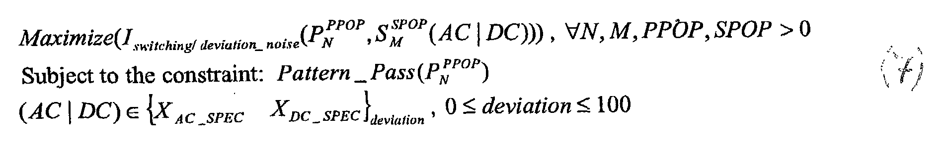
- S M SPOP (AC
- DC) (S 1 , S 2 ,..., S M ) are pre-selected, wherein M is the maximum number of worst case conditions and SPOP is a pre-selected worst case condition population. Every single condition population contains a number of pre-selected AC or DC parameters. Multiple populations form a condition code matrix (CCM) file.
- CCM condition code matrix
- worst case patterns are stored in a vector code matrix (VCM).
- VCM vector code matrix
- the function for approximating the highest switching noise is defined as a dynamic current function in respect of the switching pattern populations and the condition parameter populations subject to the constraint that the test patterns have to be valid.
- the signal switching and deviation analysis is always inside the valid range. It may be useful, however, to detect the boundaries of the valid range.
- the power supply switching and deviation noise estimation problem can be formulated as follows:
- evolutionary genetic methods are stochastic optimiziation concepts that mimic biological evolution. Such genetic concept can be employed to detect worst case switching patterns, as described above.
- the algorithm detects the best fit to the problem by evolution, i.e. processing series of test patterns in parallel.
- the test patterns are contained in test pattern populations.
- the fitness is defined as dynamic current in respect of each trial test pattern (signal switching).
- Equation (7) reflects test pattern and test condition deviation.
- the function In order to produce valid results from input signal deviation with respect to the test patterns, the function must be subjected to the constraint that the test patterns must be valid, since signal fluctuation could otherwise cause test pattern failure.
- the fitness in this embodiment is associated with the steepest maximum switching dynamic current, subject to the above mentioned constraint.
- Equation (7) is then evaluated in respect of "fitness" for each combination using ATE, and the averaged fitness of the initial population is calculated.
- the sorting function first re-arranges the test condition combination according to their fitness values from minimum to maximum. Subsequently, the parents are selected in random sequence based on the new sub-optimal fitness range. Parents (selected test condition combinations) are subjected to cross-over, recombination and/or mutation to produce offspring.
- cross-over process a method of binary cross-over is used in random sequence, and the contents of two cross-over test condition combinations are exchanged accordingly to produce new offspring combinations. Subsequently, the re-combination process is used to select the best fitness combination out of two new cross-over offspring combinations.
- the offspring After re-combination, the offspring undergoes mutation. That is, the offspring variables are mutated by the addition of small random values.
- the mutation rate ranges from -1 to 1. The mutation process helps to improve the optimization search process.
- This cycle is performed until the optimization criteria are met or the end of the optimization loop is reached. If the fitness has not improved after a pre-defined number of genetic breeding generations, a new population is generated in random sequence.
- the worst case fitness is detected automatically from all processed populations.
- the CCM database is updated accordingly.
- the above described evolution method greatly improves the chances of finding the worst case signal deviation and signal switching combination. At the same time, it is faster and more efficient than known random- or trial-based approaches.
Abstract

Description
- To achieve high perfomance and high integration density, the dimensions of integrated circuit components are scaled down more and more. In particular, transistor dimensions are scaled down while lower power dissipation is achieved by scaling down the supply voltage. However, due to high packing density of transistors, the power supply current is increasing, and hence, large current swings within a short period of time can cause considerable noise. As a consequence, one difficulty circuit designers face is the power delivery of very high performance circuits due to the severe switching noise.
- In order to verify the function of a newly designed integrated circuit, the circuit is first simulated and then tested. During simulation, multiple input signals are applied to the inputs of the circuit, and the output signals of the circuit calculated. The input signals are referred to as test patterns. If the output signals do not sufficiently approximate preset target signals, the circuit is redesigned and resimulated.
- Subsequently, when simulation is completed, a chip containing the integrated circuit is manufactured and tested using ATE (Automatic Test Equipment). The ATE also applies a test pattern to the circuit. The test pattern for the ATE has to be input manually by a user. Generally, the same test pattern that has been used for simulation is also used for testing. If the output signals generated by the circuit in response to the test pattern of the ATE deviate from preset target signals, the circuit is redesigned, resimulated and retested.
- As the complexity of integrated circuits increases, integration density and functionality increases dramatically. The simultaneous switching of a large number of transistors induces a large current spike. The switching noise on the power distribution network must be suppressed to a tolerable level to ensure the reliability of the circuit. In order to efficiently combat the switching noise, estimation of the worst case switching noise is required.
- On way of determining the worst case switching noise is to simulate all combinations of input patterns to determine which combination will induce the maximum switching noise. However, the complexity of the solution space is exponentially proportional to the number of primary inputs of the system. Accordingly, it would require an enormous time to process the entire solution space for even a moderately complex system.
- To this end, a number of approaches have been proposed to deal with these problems. In "Estimation of Switching Noise on Power Supply Lines in Deep Sub-micron CMOS circuits", Shiyou Zhao and Kaushik Roy, 13th International Conference on VLSI Design, IEEE January 2000, there is proposed a probabalistic approach to determine the lower bound of the worst case switching noise on power supply lines. The algorithm described therein traces the worst case input patterns which induces the steepest maximum switching current spike and therefore the maximum switching noise. This is based on the observation that the maximum switching noise is directly related to the steepest maximum switching current spike.
- In this approach, the design of an integrated circuit is simulated by applying randomly generated input signal vectors to the inputs of the circuit. For each input vector pair, the simulated peak switching current is determined. The worst case input vector pairs feed, as initial population, a genetic algorithm. The genetic algorithm is designed to single out the near optimal input pattern(s) that induce the steepest maximum switching current spike and, therefore, the worst case switching noise. The worst case input patterns are then used in HSPICE simulation of the circuits to extract the exact current waveform.
- One problem associated with this approach is the difficulty of generating suitable random test patterns. The larger the number of random test patterns, the higher the likelihood of generating a test pattern which approximates the worst case sufficiently. However, since the simulation of each test pattern is time consuming, the simulation of a large number number of test patterns is not practical.
- In particular, if a genetic algorithm is used, it is too time consuming to simulate every single random pattern out of every new pattern population before the algorithm is able to determine which of the patterns of the population is to be selected for further optimization. Therefore, this method becomes saturated by the number of trial random patterns in each pattern population. It is suitable for small circuits. However, it could take up to years to perform a full chip simulation of a large circuit using even the fastest simulation applications.
- The present invention aims to address this problem.
- According to one aspect of the invention, there is provided a method of generating a set of test patterns for the simulation and/or test of the layout of an integrated circuit, the method comprising the steps of:
- (a) generating a set of test patterns on a random basis;
- (b) applying the set of test patterns to the integrated circuit using automatic test equipment (ATE);
- (c) determining the outputs of the integrated circuit;
- (d) processing the outputs to determine whether predetermined test criteria are met;
- (e) depending on the determination in step (d), generating a new set of test patterns on the basis of the set of test patterns generated in step (a) using a genetic algorithm.
-
- Accordingly, the method employs a genetic algorithm (optimization method) to optimize a set of random patterns based on measurements using an ATE. Thereby, a set of worst case noise patterns can be selected automatically.
- The selected set of worst case noise patterns can be used to re-simulate the layout of the integrated circuit for detail design analysis or improvement.
- This approach is more efficient and faster than any pure random-based method employing a non-optimal random pattern generation or simulation approach.
- In addition, it can be used with any ATE system.
- A genetic algorithm can be equally employed to detect a set of potential worst case test conditions in respect of input signals supplied to an integrated circuit (e.g. power supply). The parameters of such input signals are referred to as AC/DC parameters.
- Accordingly, there is also provided a method of generating a set of input signals for the simulation and/or test of the layout of an integrated circuit, the method comprising the steps of:
- (m) generating a plurality of sets of input signals;
- (n) applying the plurality of sets of input signals to the integrated circuit using automatic test equipment (ATE);
- (o) determining the outputs of the integrated circuit;
- (p) processing the outputs to determine whether predetermined test criteria are met;
- (q) depending on the determination in step (p), generating a new plurality of sets of input signals on the basis of the plurality of sets of input signals generated in step (m) using a genetic algorithm.
-
- According to this method, a set of worst case test conditions due to resulting high power supply noise (dynamic current) can be detected without having to manually and/or randomly select parameters of input signals.
- This method may also be implemented using existing ATE systems.
- The input signals obtained as a result of this method may subsequently be re-simulated.
- Preferably, the method of approximating a worst case set of test pattern is performed together with the method of approximating a set of worst case input signals parameters. This way, an overall worst case condition of operation of the integrated circuit can be approximated.
- Exemplary embodiments of the invention will now be described by reference to the drawings, of which
- Figure 1 illustrates a schematic flow diagram of a method according to an embodiment of the invention;
- Figure 2 illustrates the results of a practical experiment using a method according to an embodiment of the invention; and
- Figure 3 illustrates a schematic flow diagram of a method according to another embodiment of the invention.
-
- Genetic algorithms are based on the principles of natural selection. In particular, genetic algorithms are stochastic search methods which simulate natural biological evolution. The algorithms operate on the basis of a population of potential solutions and, applying the principle of "survival of the fittest" to these potential solutions, produce a better approximation of a target solution in each iteration of the algorithm.
- Each iteration of the algorithm produces a new generation of approximations. The approximations of each generations are created by the process of selecting individuals according to their level of "fitness" in the problem domain. The selected individuals are bred with one another using operators borrowed from natural genetics. This process leads to the evolution of populations of individuals that are better suited for their environment than the individuals from which they were created, just as in natural adaptation.
- Accordingly, genetic algorithms model natural processes such as selection, cross over, recombination and mutation.
- Figure 1 shows a method for detecting the worst case current consumption/peak current pattern (RSMA) based on a genetic algorithm. This method operates on the basis of populations of individual patterns instead of a single pattern solution. In this way, the search for better approximations can be performed in a parallel manner. Therefore, this method is more efficient than single pattern searching processes using dynamic random algorithm methods.
- Genetic algorithms may be employed for the simulation of an integrated circuit design in order to solve the worst case pattern search problem. The efficiency of genetic searching procedures is largely dependent on the number of pattern populations and the number of test patterns in each pattern population. However, as indicated above, the simulation-based approach forms a limitation if genetic algorithms are to be employed. The genetic selection procedure has to evaluate every "fitness" (dynamic peak/averaged current)of the test patterns in each pattern population. For example, there may be 200 pattern populations each including 20 patterns. Thus, the genetic algorithm has to evaluate the fitness of 200 * 20 = 4000 patterns. If each test pattern is a 50 cycles test pattern which requires 30 minutes of simulation time (e.g. EPIC oder SPICE simulator), then the total required searching and simulation time is 4000 * 30 minutes = 120000 minutes, i.e. approximately 83 days of non stop simulation in order to process 200 pattern populations only.
- In addition, the full pattern combination domain increases proportionally to the complexity of VLSI or ULSI designs. Therefore, a subset of 200 pattern populations is only a very small subset of the full pattern combination domain.
- In contrast, when using a genetic algorithm together with ATE, many more pattern populations per time unit can be processed. This is because the testing of an integrated circuit using ATE is considerably faster than simulation using conventional systems. Accordingly, the approximation of worst case test patterns in a given period of time is much more accurate.
- An implementation of a dynamic genetic algorithm for use with ATE is presented in the following. At the beginning of the computation, a number of individual random patterns
- Subsequently, for each individual pattern (p1, p2,..., pN), the objective functions

- The first (initial) generation is thus produced, and the averaged fitness of the individual patterns (p1, p2,..., pN) is calculated using equation (2):

- If the optimization criteria
- In this selection approach, the basic concept of tournament selection is employed. That is, only the best individual pattern from the existing population is selected as a parent. This process is repeated until a pre-defined percentage of best patterns has been selected:wherein B is the pre-defined percentage of the best pattern group. The sorting function first re-arranges the test patterns from minimum to maximum according to their fitness values. Subsequently, the parent selection is generated in random sequence based on the new sub-optimal fitness range N, which is calculated using B. Parents (selected patterns) are combined using cross over (4), re-combined (5) and mutated (6) in order to produce offspring:
 where C is the test pattern content which is selected for cross over of two patterns. In the cross over process, upper, lower or stripe cross over methods are performed in random sequence, and the contents of two cross over patterns are exchanged in order to produce two new offspring patterns. Thereafter, the re-combination equation (5) is used to select the best fitness pattern out of two new cross over offspring patterns:
- The mutation process helps to improve the optimization search process.
- Finally, all offspring patterns are inserted into the population, replacing the parents (original pattern population) and producing a new generation. This cycle (loop 1 in Figure 1) is performed until the optimiziation criteria are met.
- If the fitness does not improve after a pre-defined number of genetic breeding generations, a new pattern population (loop 2 in Figure 1) will be generated in random sequence. This combination greatly increases the chances of finding worst case test patterns.
- A complete implementation of this algorithm using ATE J973 is given in Annex 1.
- Figure 2 illustrates an experimental plot of a dynamic genetic algorithm approach (100MHz, VDDP IO Pad eDRAM core). The experiment included 20 patterns in each population and 34 (population) genetic algorithm search samples (loop 2 + loop 1). The total number of patterns processed was 20 * 34 = 680. The experiment lasted considerably shorter than a simulation-based approach, and the current bound obtained through using the worst case pattern was higher compared to conventional dynamic random algorithm-based approaches.
- Another embodiment of the invention will now be described with reference to Figure 3.
- As indicated above, the maximum switching noise occuring during operation of an integrated circuit is directly related to the steepest maximum switching dynamic current spike. The switching behaviour depends on the test patterns applied to the circuit.
- In addition, the switching noise depends on the deviation of input signals (AC & DC conditions/parameters) applied to the integrated circuit. This reflects operation of integrated circuits in practice, where a 10% power supply fluctuation can occur in most applications.
- Accordingly, signal switching and deviation can have a great impact on internal signal behaviour (e.g. propagation delay) and switching noise. However, using the simulation-based approach, it is not possible to simulate millions of test patterns and different input signal conditions at the same time. Therefore, simulation-based approaches take into account signal switching only and ignore the other important cause of switching noise, namely signal deviation.
- According to the embodiment of Figure 3, a method is provided that allows for signal switching and signal deviation analysis at the same time. This results in a more efficient analysis of the operational behaviour of an integrated circuit than known methods.
- Worst case conditions of operation of an integrated circuit depends the level of switching noise. The switching noise is mainly influenced by signal switching events (different test patterns) and signal deviation (AC/DC parameter variation). In order to approximate a worst case condition, the steepest maximum switching dynamic current is to be detected. The switching dynamic current is a function of the test pattern (signal switching) and test condition variation (signal deviation). This can be subject to the constraint that the test patterns have to be valid. Alternatively, the approximation can be implemented without constraint such that the dynamic current function explores the fail region without any input signal deviation limits (e.g. +/-12.5%).
- An implementation of an approximation of worst case signal switching and deviation using a constraint optimization approach is illustrated in Figure 3. Initially, a number of individual worst case random patterns PN PPOP = (p1, p2, ..., pN) are generated using the above described method, wherein N is the maximum number of worst case patterns and PPOP is the worst case pre-selected pattern population.
- Subsequently, a number of AC or DC parameters SM SPOP (AC|DC) = (S1, S2,..., SM) are pre-selected, wherein M is the maximum number of worst case conditions and SPOP is a pre-selected worst case condition population. Every single condition population contains a number of pre-selected AC or DC parameters. Multiple populations form a condition code matrix (CCM) file.
- Similarly, worst case patterns are stored in a vector code matrix (VCM).
- The function for approximating the highest switching noise is defined as a dynamic current function in respect of the switching pattern populations and the condition parameter populations subject to the constraint that the test patterns have to be valid. Thus, the signal switching and deviation analysis is always inside the valid range. It may be useful, however, to detect the boundaries of the valid range.
- The power supply switching and deviation noise estimation problem can be formulated as follows:
- As indicated above, evolutionary genetic methods are stochastic optimiziation concepts that mimic biological evolution. Such genetic concept can be employed to detect worst case switching patterns, as described above. The algorithm detects the best fit to the problem by evolution, i.e. processing series of test patterns in parallel. The test patterns are contained in test pattern populations. The fitness is defined as dynamic current in respect of each trial test pattern (signal switching).
- Equation (7) reflects test pattern and test condition deviation. In order to produce valid results from input signal deviation with respect to the test patterns, the function must be subjected to the constraint that the test patterns must be valid, since signal fluctuation could otherwise cause test pattern failure.
- The fitness in this embodiment is associated with the steepest maximum switching dynamic current, subject to the above mentioned constraint.
- Referring more specifically to Figure 3, initially, a number of pre-selected individual test condition combinations (the population/CCM) with respect to a set of worst case patterns (VCM) are randomly generated and intialised. Equation (7) is then evaluated in respect of "fitness" for each combination using ATE, and the averaged fitness of the initial population is calculated.
- If the optimization criteria is not met (see "check evolution fitness" in Figure 3), the creation of a new population is initiated. Individual test condition combinations are selected according to their fitness for the production of offspring (Evolution Genetic Optimization Loop). In the selection approach, the basic concept of tournament selection is employed, i.e. only the best individual combination from this population is selected as parents.
- This process is repeated until a pre-defined percentage of best combinations has been selected. The sorting function first re-arranges the test condition combination according to their fitness values from minimum to maximum. Subsequently, the parents are selected in random sequence based on the new sub-optimal fitness range. Parents (selected test condition combinations) are subjected to cross-over, recombination and/or mutation to produce offspring.
- In the cross-over process, a method of binary cross-over is used in random sequence, and the contents of two cross-over test condition combinations are exchanged accordingly to produce new offspring combinations. Subsequently, the re-combination process is used to select the best fitness combination out of two new cross-over offspring combinations.
- After re-combination, the offspring undergoes mutation. That is, the offspring variables are mutated by the addition of small random values. The mutation rate ranges from -1 to 1. The mutation process helps to improve the optimization search process.
- Finally, all offspring are inserted into the population and thus replace the parents (original CCM population), producing a new population.
- This cycle is performed until the optimization criteria are met or the end of the optimization loop is reached. If the fitness has not improved after a pre-defined number of genetic breeding generations, a new population is generated in random sequence.
- At the end of the evolution loop as shown in Figure 3, the worst case fitness is detected automatically from all processed populations. The CCM database is updated accordingly.
- The whole process is repeated until all worst case patterns from the VCM file have been processed. The final worst case CCM is then generated automatically.
- The above described evolution method greatly improves the chances of finding the worst case signal deviation and signal switching combination. At the same time, it is faster and more efficient than known random- or trial-based approaches.
- It is to be noted that the invention is not restricted to the embodiments and implementations described herein but encompasses modifications and variations within the scope of the invention as determined from the claims.


Claims (24)
- A method of generating a set of test patterns for the simulation and/or test of the layout of an integrated circuit, the method comprising the steps of:(a) generating a set of test patterns on a random basis;(b) applying the set of test patterns to the integrated circuit using automatic test equipment (ATE);(c) determining the outputs of the integrated circuit;(d) processing the outputs to determine whether predetermined test criteria are met;(e) depending on the determination in step (d), generating a new set of test patterns on the basis of the set of test patterns generated in step (a) using a genetic algorithm.
- The method of claim 1, comprising:(f1) repeating steps (b) to (e) until the predetermined test criteria are met.
- The method of claim 1, comprising:(f2) repeating steps (b) to (e) for a predetermined number of times or until the predetermined test criteria are met.
- The method of claim 3, comprising:generating a new set of test patterns on a random basis, if the predetermined test criteria are not met after the repetition of steps(b) to (e) the predetermined number of times; andrepeating step (f2) on the basis of the new set of test patterns.
- The method of any of claims 2 to 4, wherein the predetermined test criteria are met if the set of test patterns is associated with an average fitness above a predetermined value.
- The method of any of claims 2 to 5, wherein step (e) comprises:combining some or all of the test patterns according to the genetic algortihm to generate the new set of test patterns.
- The method of claim 6, further comprising:selecting test patterns out of the set of test patterns according to predetermined selection criteria; andcombining the selected test patterns according to the genetic algortihm to generate the new set of test patterns.
- The method of claim 7, comprising:selecting a test pattern if it is associated with a fitness value greater than a reference value.
- The method of claim 7 or 8, comprising:(g) selecting a test pattern if it is associated with the highest fitness value of all unselected test patterns.
- The method of claim 9, comprising:repeating step (g) until a predetermined percentage of test patterns has been selected.
- The method of claim 9, wherein step (e) comprises:(h) arranging the selected test patterns in the order of associated fitness values;(i) randomly selecting parent test patterns out of the test patterns as arranged in step (h); and(j) combining the selected parent test patterns.
- The method of any preceding claim, wherein the genetic algorithm includes crossing over, re-combination, and/or mutation of selected test patterns.
- The method of any preceding claim, wherein step (a) comprises:generating a plurality of sets of test patterns, wherein each set of test patterns is included in a test pattern population.
- The method of claim 13, comprising:performing the steps of any of the preceding claim for each population.
- A method of generating a set of input signals for the simulation and/or test of the layout of an integrated circuit, the method comprising the steps of:(m) generating a plurality of sets of input signals;(n) applying the plurality of sets of input signals to the integrated circuit using automatic test equipment (ATE);(o) determining the outputs of the integrated circuit;(p) processing the outputs to determine whether predetermined test criteria are met;(q) depending on the determination in step (p), generating a new plurality of sets of input signals on the basis of the plurality of sets of input signals generated in step (m) using a genetic algorithm.
- The method of claim 15, wherein the input signals are associated with a number of AC/DC parameters.
- The method of claim 15 or 16, wherein predetermined parameters of each set of input signals vary from those of other sets of input signals.
- The method of any of claims 15 to 17, comprising:(r1) repeating steps (n) to (q) until the predetermined test criteria are met.
- The method of any of claims 15 to 17, comprising:(r2) repeating steps (n) to (q) for a predetermined number of times or until the predetermined test criteria are met.
- The method of any of claims 15 to 19, wherein the predetermined test criteria are met if the plurality of sets of input signals is associated with a worst case of operation situation.
- The method of any of claims 15 to 20, wherein step (q) comprises:combining some or all of corresponding input signals of different sets of input signals according to the genetic algortihm to generate a new set of input signals.
- A method of generating test patterns and input signals for the simulation and/or test of the layout of an integrated circuit, the method comprising:performing the method of any of claims 1 to 14; andperforming the method of any of claims 15 to 21.
- A data processing system comprising an automatic test equipment (ATE), the data processing system being arranged to perform the method of any preceding claim.
- A computer program adapted to perform the method of any of the claims 1 to 22 on a computer associated with an automatic test equipment (ATE).
Priority Applications (3)
| Application Number | Priority Date | Filing Date | Title |
|---|---|---|---|
| EP02090271A EP1382975B1 (en) | 2002-07-19 | 2002-07-19 | Method of generating a test pattern for the simulation and/or test of the layout of an integrated circuit |
| DE60224378T DE60224378T2 (en) | 2002-07-19 | 2002-07-19 | Method for generating a test pattern for the simulation and / or testing of the layout of an integrated circuit |
| US10/623,067 US6993735B2 (en) | 2002-07-19 | 2003-07-18 | Method of generating a test pattern for simulating and/or testing the layout of an integrated circuit |
Applications Claiming Priority (1)
| Application Number | Priority Date | Filing Date | Title |
|---|---|---|---|
| EP02090271A EP1382975B1 (en) | 2002-07-19 | 2002-07-19 | Method of generating a test pattern for the simulation and/or test of the layout of an integrated circuit |
Publications (2)
| Publication Number | Publication Date |
|---|---|
| EP1382975A1 true EP1382975A1 (en) | 2004-01-21 |
| EP1382975B1 EP1382975B1 (en) | 2008-01-02 |
Family
ID=29762697
Family Applications (1)
| Application Number | Title | Priority Date | Filing Date |
|---|---|---|---|
| EP02090271A Expired - Fee Related EP1382975B1 (en) | 2002-07-19 | 2002-07-19 | Method of generating a test pattern for the simulation and/or test of the layout of an integrated circuit |
Country Status (3)
| Country | Link |
|---|---|
| US (1) | US6993735B2 (en) |
| EP (1) | EP1382975B1 (en) |
| DE (1) | DE60224378T2 (en) |
Cited By (2)
| Publication number | Priority date | Publication date | Assignee | Title |
|---|---|---|---|---|
| EP1577801A1 (en) * | 2004-03-15 | 2005-09-21 | Infineon Technologies AG | Device characterization concept |
| CN103869709A (en) * | 2012-12-13 | 2014-06-18 | 英飞凌科技股份有限公司 | Emulation system and method |
Families Citing this family (9)
| Publication number | Priority date | Publication date | Assignee | Title |
|---|---|---|---|---|
| US7120840B1 (en) * | 2004-02-06 | 2006-10-10 | Credence Systems Corporation | Method and system for improved ATE timing calibration at a device under test |
| JP4414899B2 (en) * | 2005-01-17 | 2010-02-10 | Okiセミコンダクタ株式会社 | How to place dummy metal |
| US20060195744A1 (en) * | 2005-02-11 | 2006-08-31 | Broadcom Corporation | Method and apparatus to simulate automatic test equipment |
| US7313771B2 (en) * | 2005-03-31 | 2007-12-25 | Fujitsu Limited | Computing current in a digital circuit based on an accurate current model for library cells |
| US7844926B1 (en) * | 2006-01-31 | 2010-11-30 | Oracle America, Inc. | Specification window violation identification with application in semiconductor device design |
| US20070266349A1 (en) * | 2006-05-09 | 2007-11-15 | Craig Jesse E | Directed random verification |
| US20080046789A1 (en) * | 2006-08-21 | 2008-02-21 | Igor Arsovski | Apparatus and method for testing memory devices and circuits in integrated circuits |
| US7615990B1 (en) | 2007-06-28 | 2009-11-10 | Credence Systems Corporation | Loadboard enhancements for automated test equipment |
| US20110126052A1 (en) * | 2009-11-23 | 2011-05-26 | Bhavesh Mistry | Generation of Test Information for Testing a Circuit |
Family Cites Families (6)
| Publication number | Priority date | Publication date | Assignee | Title |
|---|---|---|---|---|
| US6311318B1 (en) * | 1999-07-13 | 2001-10-30 | Vlsi Technology, Inc. | Design for test area optimization algorithm |
| US6327687B1 (en) * | 1999-11-23 | 2001-12-04 | Janusz Rajski | Test pattern compression for an integrated circuit test environment |
| CA2321346A1 (en) * | 2000-09-28 | 2002-03-28 | Stephen K. Sunter | Method, system and program product for testing and/or diagnosing circuits using embedded test controller access data |
| US6782515B2 (en) * | 2002-01-02 | 2004-08-24 | Cadence Design Systems, Inc. | Method for identifying test points to optimize the testing of integrated circuits using a genetic algorithm |
| US7039845B2 (en) * | 2002-03-28 | 2006-05-02 | Jeff Rearick | Method and apparatus for deriving a bounded set of path delay test patterns covering all transition faults |
| GB0213882D0 (en) * | 2002-06-17 | 2002-07-31 | Univ Strathclyde | A digital system & method for testing analogue & mixed-signal circuits or systems |
-
2002
- 2002-07-19 DE DE60224378T patent/DE60224378T2/en not_active Expired - Lifetime
- 2002-07-19 EP EP02090271A patent/EP1382975B1/en not_active Expired - Fee Related
-
2003
- 2003-07-18 US US10/623,067 patent/US6993735B2/en not_active Expired - Fee Related
Non-Patent Citations (3)
| Title |
|---|
| M.S. HSIAO, ET AL.: "Sequential Circuit Test Generation using dynamic state traversal", EUROPEAN DESIGN AND TEST CONFERENCE., March 1997 (1997-03-01), pages 22 - 28, XP002235153 * |
| P. MAZUMDER, E. RUDNICK: "Genetic Algorithms for VLSI Design, Layout & Test Automation", 1999, PRENTICE HALL, UPPER SADDLE RIVER, NJ, USA, XP002235155 * |
| STEVEN SINGER, LARRY VENETSKY & MICHAEL L. LYNCH: "Virtual Test Automation Generator (VTAG)", NAVAIR LAKEHURST, 5 May 2000 (2000-05-05), XP002235154, Retrieved from the Internet <URL:http://www.lakehurst.navy.mil/vtag.pdf> [retrieved on 20030318] * |
Cited By (2)
| Publication number | Priority date | Publication date | Assignee | Title |
|---|---|---|---|---|
| EP1577801A1 (en) * | 2004-03-15 | 2005-09-21 | Infineon Technologies AG | Device characterization concept |
| CN103869709A (en) * | 2012-12-13 | 2014-06-18 | 英飞凌科技股份有限公司 | Emulation system and method |
Also Published As
| Publication number | Publication date |
|---|---|
| DE60224378D1 (en) | 2008-02-14 |
| US20040034838A1 (en) | 2004-02-19 |
| US6993735B2 (en) | 2006-01-31 |
| DE60224378T2 (en) | 2009-01-02 |
| EP1382975B1 (en) | 2008-01-02 |
Similar Documents
| Publication | Publication Date | Title |
|---|---|---|
| EP1382975A1 (en) | Method of generating a test pattern for the simulation and/or test of the layout of an integrated circuit | |
| US20180100894A1 (en) | Automatic Generation of Test Sequences | |
| US8875077B1 (en) | Fault sensitivity analysis-based cell-aware automated test pattern generation flow | |
| US6810372B1 (en) | Multimodal optimization technique in test generation | |
| Zhao et al. | A genetic algorithm based remaining lifetime prediction for a VLIW processor employing path delay and IDDX testing | |
| CN109886328B (en) | Electric vehicle charging facility fault prediction method and system | |
| US20220067255A1 (en) | Dynamic current modeling in dynamic voltage drop analysis | |
| Corno et al. | GARDA: A diagnostic ATPG for large synchronous sequential circuits | |
| EP1382976B1 (en) | Method of processing test patterns for an integrated circuit | |
| CN106600119B (en) | K-means-based power consumer clustering method and device | |
| Šikulová et al. | Coevolution in cartesian genetic programming | |
| Habibi et al. | Towards an efficient assertion based verification of SystemC designs | |
| Santos et al. | Defect-oriented verilog fault simulation of SoC macros using a stratified fault sampling technique | |
| Braun et al. | Comparison of Bayesian networks and data mining for coverage directed verification category simulation-based verification | |
| Pradhan et al. | Low power and high testable Finite State Machine synthesis | |
| Varambally et al. | Optimising design verification using machine learning: An open source solution | |
| Bogdan et al. | On the Empirical Bayes approach to the problem of multiple testing | |
| MacEachern | Constrained circuit optimization via library table genetic algorithms | |
| CN107491384A (en) | Information processor, information processing method and message processing device | |
| Golonek et al. | Optimization of PWL analog testing excitation by means of genetic algorithm | |
| Drechsler et al. | Genetic Alogrithms in Computer Aided Design of Integrated Circuits | |
| Deyati et al. | TRAP: Test generation driven classification of analog/RF ICs using adaptive probabilistic clustering algorithm | |
| Hudec | An efficient adaptive method of software-based self test generation for RISC processors | |
| Wang et al. | Generating high-quality random numbers by cellular automata with PSO | |
| Vinay et al. | Evolutionary Testing Techniques for Sequential Circuits |
Legal Events
| Date | Code | Title | Description |
|---|---|---|---|
| PUAI | Public reference made under article 153(3) epc to a published international application that has entered the european phase |
Free format text: ORIGINAL CODE: 0009012 |
|
| AK | Designated contracting states |
Kind code of ref document: A1 Designated state(s): AT BE BG CH CY CZ DE DK EE ES FI FR GB GR IE IT LI LU MC NL PT SE SK TR |
|
| AX | Request for extension of the european patent |
Extension state: AL LT LV MK RO SI |
|
| 17P | Request for examination filed |
Effective date: 20040217 |
|
| AKX | Designation fees paid |
Designated state(s): DE FR GB |
|
| RBV | Designated contracting states (corrected) |
Designated state(s): DE GB IE |
|
| GRAP | Despatch of communication of intention to grant a patent |
Free format text: ORIGINAL CODE: EPIDOSNIGR1 |
|
| RAP1 | Party data changed (applicant data changed or rights of an application transferred) |
Owner name: QIMONDA AG |
|
| GRAS | Grant fee paid |
Free format text: ORIGINAL CODE: EPIDOSNIGR3 |
|
| GRAA | (expected) grant |
Free format text: ORIGINAL CODE: 0009210 |
|
| AK | Designated contracting states |
Kind code of ref document: B1 Designated state(s): DE GB IE |
|
| REG | Reference to a national code |
Ref country code: GB Ref legal event code: FG4D |
|
| REG | Reference to a national code |
Ref country code: IE Ref legal event code: FG4D |
|
| REF | Corresponds to: |
Ref document number: 60224378 Country of ref document: DE Date of ref document: 20080214 Kind code of ref document: P |
|
| PLBE | No opposition filed within time limit |
Free format text: ORIGINAL CODE: 0009261 |
|
| STAA | Information on the status of an ep patent application or granted ep patent |
Free format text: STATUS: NO OPPOSITION FILED WITHIN TIME LIMIT |
|
| 26N | No opposition filed |
Effective date: 20081003 |
|
| GBPC | Gb: european patent ceased through non-payment of renewal fee |
Effective date: 20080719 |
|
| PG25 | Lapsed in a contracting state [announced via postgrant information from national office to epo] |
Ref country code: GB Free format text: LAPSE BECAUSE OF NON-PAYMENT OF DUE FEES Effective date: 20080719 |
|
| PG25 | Lapsed in a contracting state [announced via postgrant information from national office to epo] |
Ref country code: IE Free format text: LAPSE BECAUSE OF NON-PAYMENT OF DUE FEES Effective date: 20080721 |
|
| REG | Reference to a national code |
Ref country code: DE Ref legal event code: R081 Ref document number: 60224378 Country of ref document: DE Owner name: INFINEON TECHNOLOGIES AG, DE Free format text: FORMER OWNER: QIMONDA AG, 81739 MUENCHEN, DE Ref country code: DE Ref legal event code: R081 Ref document number: 60224378 Country of ref document: DE Owner name: POLARIS INNOVATIONS LTD., IE Free format text: FORMER OWNER: QIMONDA AG, 81739 MUENCHEN, DE |
|
| REG | Reference to a national code |
Ref country code: DE Ref legal event code: R081 Ref document number: 60224378 Country of ref document: DE Owner name: POLARIS INNOVATIONS LTD., IE Free format text: FORMER OWNER: INFINEON TECHNOLOGIES AG, 85579 NEUBIBERG, DE |
|
| PGFP | Annual fee paid to national office [announced via postgrant information from national office to epo] |
Ref country code: DE Payment date: 20150930 Year of fee payment: 14 |
|
| REG | Reference to a national code |
Ref country code: DE Ref legal event code: R119 Ref document number: 60224378 Country of ref document: DE |
|
| PG25 | Lapsed in a contracting state [announced via postgrant information from national office to epo] |
Ref country code: DE Free format text: LAPSE BECAUSE OF NON-PAYMENT OF DUE FEES Effective date: 20170201 |