EP1381023A2 - Common electrode voltage driving circuit for liquid crystal display and adjusting method of the same - Google Patents
Common electrode voltage driving circuit for liquid crystal display and adjusting method of the same Download PDFInfo
- Publication number
- EP1381023A2 EP1381023A2 EP03013840A EP03013840A EP1381023A2 EP 1381023 A2 EP1381023 A2 EP 1381023A2 EP 03013840 A EP03013840 A EP 03013840A EP 03013840 A EP03013840 A EP 03013840A EP 1381023 A2 EP1381023 A2 EP 1381023A2
- Authority
- EP
- European Patent Office
- Prior art keywords
- common electrode
- liquid crystal
- electrode signal
- vcom
- crystal display
- Prior art date
- Legal status (The legal status is an assumption and is not a legal conclusion. Google has not performed a legal analysis and makes no representation as to the accuracy of the status listed.)
- Withdrawn
Links
Images


Classifications
-
- G—PHYSICS
- G09—EDUCATION; CRYPTOGRAPHY; DISPLAY; ADVERTISING; SEALS
- G09G—ARRANGEMENTS OR CIRCUITS FOR CONTROL OF INDICATING DEVICES USING STATIC MEANS TO PRESENT VARIABLE INFORMATION
- G09G3/00—Control arrangements or circuits, of interest only in connection with visual indicators other than cathode-ray tubes
- G09G3/20—Control arrangements or circuits, of interest only in connection with visual indicators other than cathode-ray tubes for presentation of an assembly of a number of characters, e.g. a page, by composing the assembly by combination of individual elements arranged in a matrix no fixed position being assigned to or needed to be assigned to the individual characters or partial characters
- G09G3/34—Control arrangements or circuits, of interest only in connection with visual indicators other than cathode-ray tubes for presentation of an assembly of a number of characters, e.g. a page, by composing the assembly by combination of individual elements arranged in a matrix no fixed position being assigned to or needed to be assigned to the individual characters or partial characters by control of light from an independent source
- G09G3/36—Control arrangements or circuits, of interest only in connection with visual indicators other than cathode-ray tubes for presentation of an assembly of a number of characters, e.g. a page, by composing the assembly by combination of individual elements arranged in a matrix no fixed position being assigned to or needed to be assigned to the individual characters or partial characters by control of light from an independent source using liquid crystals
-
- G—PHYSICS
- G09—EDUCATION; CRYPTOGRAPHY; DISPLAY; ADVERTISING; SEALS
- G09G—ARRANGEMENTS OR CIRCUITS FOR CONTROL OF INDICATING DEVICES USING STATIC MEANS TO PRESENT VARIABLE INFORMATION
- G09G3/00—Control arrangements or circuits, of interest only in connection with visual indicators other than cathode-ray tubes
- G09G3/20—Control arrangements or circuits, of interest only in connection with visual indicators other than cathode-ray tubes for presentation of an assembly of a number of characters, e.g. a page, by composing the assembly by combination of individual elements arranged in a matrix no fixed position being assigned to or needed to be assigned to the individual characters or partial characters
- G09G3/34—Control arrangements or circuits, of interest only in connection with visual indicators other than cathode-ray tubes for presentation of an assembly of a number of characters, e.g. a page, by composing the assembly by combination of individual elements arranged in a matrix no fixed position being assigned to or needed to be assigned to the individual characters or partial characters by control of light from an independent source
- G09G3/36—Control arrangements or circuits, of interest only in connection with visual indicators other than cathode-ray tubes for presentation of an assembly of a number of characters, e.g. a page, by composing the assembly by combination of individual elements arranged in a matrix no fixed position being assigned to or needed to be assigned to the individual characters or partial characters by control of light from an independent source using liquid crystals
- G09G3/3611—Control of matrices with row and column drivers
- G09G3/3648—Control of matrices with row and column drivers using an active matrix
- G09G3/3655—Details of drivers for counter electrodes, e.g. common electrodes for pixel capacitors or supplementary storage capacitors
-
- G—PHYSICS
- G09—EDUCATION; CRYPTOGRAPHY; DISPLAY; ADVERTISING; SEALS
- G09G—ARRANGEMENTS OR CIRCUITS FOR CONTROL OF INDICATING DEVICES USING STATIC MEANS TO PRESENT VARIABLE INFORMATION
- G09G2300/00—Aspects of the constitution of display devices
- G09G2300/08—Active matrix structure, i.e. with use of active elements, inclusive of non-linear two terminal elements, in the pixels together with light emitting or modulating elements
-
- G—PHYSICS
- G09—EDUCATION; CRYPTOGRAPHY; DISPLAY; ADVERTISING; SEALS
- G09G—ARRANGEMENTS OR CIRCUITS FOR CONTROL OF INDICATING DEVICES USING STATIC MEANS TO PRESENT VARIABLE INFORMATION
- G09G2320/00—Control of display operating conditions
- G09G2320/02—Improving the quality of display appearance
- G09G2320/0223—Compensation for problems related to R-C delay and attenuation in electrodes of matrix panels, e.g. in gate electrodes or on-substrate video signal electrodes
-
- G—PHYSICS
- G09—EDUCATION; CRYPTOGRAPHY; DISPLAY; ADVERTISING; SEALS
- G09G—ARRANGEMENTS OR CIRCUITS FOR CONTROL OF INDICATING DEVICES USING STATIC MEANS TO PRESENT VARIABLE INFORMATION
- G09G2320/00—Control of display operating conditions
- G09G2320/06—Adjustment of display parameters
- G09G2320/0693—Calibration of display systems
-
- G—PHYSICS
- G09—EDUCATION; CRYPTOGRAPHY; DISPLAY; ADVERTISING; SEALS
- G09G—ARRANGEMENTS OR CIRCUITS FOR CONTROL OF INDICATING DEVICES USING STATIC MEANS TO PRESENT VARIABLE INFORMATION
- G09G2370/00—Aspects of data communication
- G09G2370/04—Exchange of auxiliary data, i.e. other than image data, between monitor and graphics controller
- G09G2370/042—Exchange of auxiliary data, i.e. other than image data, between monitor and graphics controller for monitor identification
-
- G—PHYSICS
- G09—EDUCATION; CRYPTOGRAPHY; DISPLAY; ADVERTISING; SEALS
- G09G—ARRANGEMENTS OR CIRCUITS FOR CONTROL OF INDICATING DEVICES USING STATIC MEANS TO PRESENT VARIABLE INFORMATION
- G09G3/00—Control arrangements or circuits, of interest only in connection with visual indicators other than cathode-ray tubes
- G09G3/006—Electronic inspection or testing of displays and display drivers, e.g. of LED or LCD displays
-
- G—PHYSICS
- G09—EDUCATION; CRYPTOGRAPHY; DISPLAY; ADVERTISING; SEALS
- G09G—ARRANGEMENTS OR CIRCUITS FOR CONTROL OF INDICATING DEVICES USING STATIC MEANS TO PRESENT VARIABLE INFORMATION
- G09G5/00—Control arrangements or circuits for visual indicators common to cathode-ray tube indicators and other visual indicators
- G09G5/003—Details of a display terminal, the details relating to the control arrangement of the display terminal and to the interfaces thereto
-
- Y—GENERAL TAGGING OF NEW TECHNOLOGICAL DEVELOPMENTS; GENERAL TAGGING OF CROSS-SECTIONAL TECHNOLOGIES SPANNING OVER SEVERAL SECTIONS OF THE IPC; TECHNICAL SUBJECTS COVERED BY FORMER USPC CROSS-REFERENCE ART COLLECTIONS [XRACs] AND DIGESTS
- Y10—TECHNICAL SUBJECTS COVERED BY FORMER USPC
- Y10S—TECHNICAL SUBJECTS COVERED BY FORMER USPC CROSS-REFERENCE ART COLLECTIONS [XRACs] AND DIGESTS
- Y10S345/00—Computer graphics processing and selective visual display systems
- Y10S345/904—Display with fail/safe testing feature
Definitions
- This invention relates to a liquid crystal display device in which a common electrode signal Vcom of the display panel of the display device is easily adjusted by a manufacture of the liquid crystal display device, and an adjusting method thereof.
- FIG. 8 shows an equivalent circuit diagram of a pixel of a liquid crystal panel according to the conventional art. Such pixels are disposed in a matrix of m rows and n columns. A gate signal line 50 and a drain signal line 51 are formed on an insulating substrate (not shown), intersecting each other. A pixel selecting thin film transistor 52 connected to both the lines 50 and 51 is provided in a periphery of the intersection of those lines. A common electrode signal Vcom is applied to a common electrode of a liquid crystal 53.
- a storage capacitance element 55 for storing a voltage of a display electrode 54 for one field is provided.
- a terminal 56 on one side of the storage capacitance element 55 is connected to a source 52s of the pixel selecting TFT 52, and an electrode 57 on another side of the storage capacitance element 55 is applied with an electric potential common to the pixels.
- the pixel selecting TFT 52 turns on so that a video signal Sig is transmitted from the drain signal line 51 to the display electrode 54 and stored in the storage capacitance element 55.
- the video signal Sig applied to the display electrode 54 is applied to the liquid crystal 53, and the liquid crystal 53 is aligned in response to the signal voltage.
- a line inversion driving method in which the polarity of the video signal Sig is reversed every 1H period is employed. In this method, it is necessary to set the video signal Sig so as to change symmetrically with respect to the common electrode signal Vcom in order to avoid generating of the DC component.
- the voltage applied to the liquid crystal 53 is lowered by ⁇ V as shown in Figs. 9 and 10.
- a parasitic capacitance 60 is formed between the gate and the source 52s of the pixel selecting TFT 52 so that the source 11s is lowered by ⁇ V by capacitance coupling, when the gate scanning signal Vg changes from a high level to a low level.
- the common electrode signal Vcom also needs to be lowered by ⁇ V (to Vcom' in Fig. 10).
- the common electrode signal Vcom needs to be adjusted for each of the liquid crystal panels.
- Fig. 11 is a flowchart showing a production flow from manufacturing of the liquid crystal panel by a liquid crystal panel manufacturer to shipping the product to the market by an assembling manufacturer.
- liquid crystal panels are manufactured (step 1), inspected (step 2), and shipped to the assembling manufacturer (step 3).
- the assembling manufacturer which receives the liquid crystal panels, detects and sets an optimum common electrode signal Vcom for each of the liquid crystal panels (step 4). It has been known as a detecting method of the optimum value of the common electrode signal Vcom to scan the common electrode signal Vcom while monitoring brightness of the liquid crystal panel and set the common electrode signal Vcom when the brightness is at the minimum as the optimum common electrode signal Vcom.
- Each of the liquid crystal panels which is set with the optimum common electrode signal Vcom, is assembled in a set such as a TV set or a cellular phone (step 5), and then shipped to the market (step 6).
- the assembling manufacturer needs to detect the optimum value of the common electrode signal Vcom for the liquid crystal panel and set it therein, the assembling manufacturer is burdened with many manufacturing steps.
- the object of this invention is directed to a liquid crystal display device in which the assembling manufacturer using the liquid crystal panel can easily set the optimum value of the common electrode signal Vcom, and an adjusting method of the liquid crystal display device.
- the invention provides a liquid crystal display device that includes a liquid crystal panel, a common electrode signal generating circuit generating a common electrode signal applied to a common electrode of the liquid crystal panel, and a non-volatile memory storing a code corresponding to a value of the common electrode signal.
- the common electrode signal generating circuit generates the common electrode signal corresponding to the code read out from the non-volatile memory.
- the invention also provides an adjusting method of a liquid crystal display device.
- the device includes a liquid crystal panel, a common electrode signal generating circuit generating a common electrode signal applied to a common electrode of the liquid crystal panel, and a non-volatile memory storing a code corresponding to a value of the common electrode signal.
- the method includes inspecting the liquid crystal panel to detect the value of the common electrode signal, encoding the value of the common electrode signal into the code, inputting the code to the non-volatile memory, reading out the code from the non-volatile memory, and controlling the common electrode signal generating circuit based on the code.
- the invention further provides an adjusting method of a liquid crystal display device.
- the device includes a liquid crystal panel, a common electrode signal generating circuit generating a common electrode signal applied to a common electrode of the liquid crystal panel, a non-volatile memory storing a code corresponding to a value of the common electrode signal, and a CPU decoding the code read out from the non-volatile memory and outputting a command to control the common electrode signal generating circuit to the common electrode signal generating circuit based on a result of the decoding.
- the method includes inspecting the liquid crystal panel to detect the value of the common electrode signal, encoding the value of the common electrode signal into the code, inputting the code to the non-volatile memory, reading out the code from the non-volatile memory and sending the code to the CPU, and decoding the code at the CPU and outputting the command to control the common electrode signal generating circuit to the common electrode signal generating circuit based on the result of the decoding.
- the invention yet further provides an adjusting method of a liquid crystal display device that includes a liquid crystal panel and a common electrode signal generating circuit generating a common electrode signal applied to a common electrode of the liquid crystal panel.
- the method includes detecting a value of the common electrode signal at an inspection by a supplier of the liquid crystal panel, supplying data representing the value of the common electrode signal to a manufacturer of the liquid crystal display device who assembles the liquid crystal panel into the liquid crystal display device, and adjusting the common electrode signal generating circuit by using the data representing the value of the common electrode signal at a manufacturing step of the liquid crystal display device by the manufacturer.
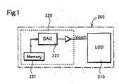
- FIG. 1 is a block diagram of a liquid crystal module.
- the liquid crystal module 200 is provided with a liquid crystal panel 210, and a control IC 220 for controlling a display of the liquid crystal panel 210 by supplying a video signal Sig, a common electrode signal Vcom, and other various drive signals to the liquid crystal panel 210.
- the liquid crystal panel 210 is provided with a pixel region in which, for example, the pixels shown in Fig. 8 are disposed in a matrix of m rows and n columns, and a horizontal scanner, a vertical scanner or the like, which are not shown, disposed in a periphery of the pixel region.
- the control IC 220 has a non-volatile memory 221 for storing an ID code of n bit corresponding to an optimum value of the common electrode signal Vcom, and a DA converter 222 (common electrode signal generating circuit) for generating the common electrode signal Vcom of the optimum value corresponding to the ID code read out from the non-volatile memory 221.
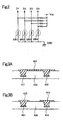
- Fig. 2 is a circuit diagram of the non-volatile memory 221.
- This circuit is a non-volatile memory with four jumper switches SW1 to SW4, and one ends of the four jumper switches SW1 to SW4 are grounded to the GND (ground potential) and other ends of the switches are provided with a power supply voltage VDD.
- the ID code of four bits (D1, D2, D3, and D4) is stored. Each bit corresponds to closing or opening of the jumper switches SW1 to SW4. For example, when SW1 is closed or in a connected state, a VDD level is outputted, and when SW1 is open or in a disconnected state, a GND level is outputted. Therefore, a binary signal can be stored as D1.
- Figs. 3A and 3B are cross-sectional views of the jumper switches SW1 to SW4.
- a resistance line 403 made of, for example, solder is connected to pad electrodes 401 and 402 buried in an insulating substrate 400, the pad electrodes 401 and 402 being spaced to each other.
- the resistance line 403 can be easily and mechanically disconnected. This method using the jumper switches SW1 to SW4 costs less and provides high working efficiency.
- the non-volatile memory 221 is not limited to this, but may be, for example, an EPROM or an EEPROM in which the ID code can be electrically written in and read out.
- the non-volatile memory 221 may be incorporated into the control IC 220 or provided outside of the control IC 220.
- Fig. 4 is a flowchart showing an adjusting method of the above described common electrode signal Vcom of the liquid crystal module 200, based on the constructions shown in Figs. 1-3B.
- the liquid crystal modules 200 each of which is mounted with the liquid crystal panel 210 and the control IC 220, are manufactured by a liquid crystal panel manufacturer (step 100).
- the liquid crystal panels 210 in the modules are each inspected and the optimum values of the common electrode signals Vcoms are each detected (step 101).
- the detecting method of the optimum value of the common electrode signal Vcom there is employed the method in which the common electrode signal Vcom is scanned while monitoring brightness of a screen of the liquid crystal panel 210, and set the signal when the brightness is at the minimum as the optimum common electrode signal Vcom.
- An operator refers to a prepared table for matching the common electrode signals Vcoms with the ID codes, and the ID codes corresponding to the detected optimum values of the common electrode signals Vcoms are each stored, for example, in each of the above described non-volatile memories 221 made of the jumper switches SW1 to SW4.
- the liquid crystal panel manufacturer ships the liquid crystal modules 200 stored with the ID codes to an assembling manufacturer (step 103).
- the assembling manufacturer which receives the liquid crystal modules 200, turns on the control ICs 220, the ID codes are each read out from the non-volatile memories 221 and converted at the DA converters 222, thereby automatically generating the optimum common electrode signals Vcoms (step 104).
- each of the liquid crystal panels severally set with the optimum common electrode signal Vcom is assembled in a set such as a TV set and a cellular phone (step 105) and then shipped to the market (step 106). This reduces the process of detecting and setting the common electrode signals Vcoms on the side of the assembling manufacturer.
- FIG. 5 is a block diagram of a liquid crystal module 200A.
- the liquid crystal module 200A is different from the liquid crystal module 200 of Fig. 1 in that a CPU interface 223 is provided in the control IC 220A and to enable data-communication with a CPU 300 on the side of the assembling manufacturer.
- the ID code read out from the non-volatile memory 221 is sent through the CPU interface 223 to the CPU 300, and decoded at the CPU 300.
- the CPU 300 sends a control command corresponding to the decoded result through the CPU interface 223 to the DA converter 222.
- This configuration enhances flexibility of adjusting the common electrode signal Vcom on the side of the assembling manufacturer, as compared with the first embodiment. That is, in the first embodiment, since the ID code read out from the non-volatile memory 221 is directly converted from a digital signal to an analog signal at the DA converter 222, one common electrode signal Vcom corresponds to one ID code. On the other hand, in this embodiment, changing the program which drives the CPU 300 enables to generate an arbitrary common electrode signal Vcom corresponding to one ID code.
- Fig. 6 is a flowchart showing an adjusting method of the common electrode signal Vcom.
- This adjusting method may be applied to a liquid crystal module 200B provided with a control IC 220B which does not have the non-volatile memory as shown in Fig. 7.
- the ID code is applied from an external terminal 230 to a DA converter 222A to generate the common electrode signal Vcom.
- this adjusting method can be applied to the liquid crystal modules 200 and 200A in the first and second embodiments.
- the liquid crystal modules 200B each of which is mounted with the liquid crystal panel 210 and the control IC 220B are manufactured (step 500). Then, the liquid crystal panels 210 in the modules are each inspected, and the optimum values of the common electrode signals Vcoms are each detected (step 501).
- the detecting method of the optimum value of the common electrode signal Vcom there is employed the method in which the common electrode signal Vcom is scanned while monitoring brightness of a screen of the liquid crystal panel 210, and set the signal when the brightness is at the minimum as the optimum common electrode signal Vcom.
- An operator refers to a prepared table for matching the common electrode signals Vcoms with the ID codes, and encodes the optimum values of the detected common electrode signals Vcoms into ID codes.
- ID code data which is a table of serial numbers and the ID codes (which corresponds to the optimum values of the common electrode signals Vcoms) of the liquid crystal modules 200B, is sent to the assembling manufacturer (step 502).
- the table for matching the common electrode signals Vcoms with the ID codes is sent to the assembling manufacturer in advance or sent with the above ID code data.
- the data can be sent by mail, facsimile, or electronic mail
- sending the data to a computer of the assembling manufacturer by a predetermined form of an electronic file provides an advantage that the assembling manufacturer can use the data to automate the adjusting work of the common electrode signals Vcoms.
- the liquid crystal modules 200B each of which is mounted with the liquid crystal panel 210 and the control IC 220B are sent to the assembling manufacturer (step 503).
- the above described ID code data is applied to the DA converters 222A to generate the optimum common electrode signals Vcoms.
- Each of the liquid crystal panels severally set with the common electrode signal Vcom is assembled in a set such as a TV set and a cellular phone (step 505), and then shipped to the market (step 506). This reduces the process of detecting and setting the common electrode signals Vcoms on the side of the assembling manufacturer.
Landscapes
- Engineering & Computer Science (AREA)
- Chemical & Material Sciences (AREA)
- Crystallography & Structural Chemistry (AREA)
- Physics & Mathematics (AREA)
- Computer Hardware Design (AREA)
- General Physics & Mathematics (AREA)
- Theoretical Computer Science (AREA)
- Power Engineering (AREA)
- Control Of Indicators Other Than Cathode Ray Tubes (AREA)
- Liquid Crystal Display Device Control (AREA)
- Liquid Crystal (AREA)
Abstract
Description
Claims (12)
- A liquid crystal display device comprising:wherein the common electrode signal generating circuit (222) generates the common electrode signal (Vcom) corresponding to the code read out from the non-volatile memory (221).a liquid crystal panel (210);a common electrode signal generating circuit (222) generating a common electrode signal (Vcom) applied to a common electrode of the liquid crystal panel (210); anda non-volatile memory (221) storing a code corresponding to a value of the common electrode signal (Vcom),
- The liquid crystal display device of claim 1 or 2, further comprising a CPU (300) decoding the code read out from the non-volatile memory (221) and supplying a command for controlling the common electrode signal generating circuit (222) to the common electrode signal generating circuit (222) based on a result of the decoding.
- The liquid crystal display device of claim 1 or 2, wherein the non-volatile memory (221) comprises a jumper switching circuit (SW1-4).
- The liquid crystal display device of claim 1 or 2, wherein the non-volatile memory (221) comprises an EPROM or an EEPROM.
- The liquid crystal display device according to any of claims 1 to 4, wherein the value of the common electrode signal (Vcom) is an optimum common electrode signal measured.
- An adjusting method of a liquid crystal display device, the device comprising a liquid crystal panel (210), a common electrode signal generating circuit (222) generating a common electrode signal (Vcom) applied to a common electrode of the liquid crystal panel (210), and a non-volatile memory (221) storing a code corresponding to a value of the common electrode signal (Vcom), the method comprising:inspecting (101) the liquid crystal panel to detect the value of the common electrode signal (Vcom);encoding the value of the common electrode signal (Vcom) into the code;inputting (102) the code to the non-volatile memory (221);reading out the code from the non-volatile memory; andcontrolling (104) the common electrode signal generating circuit (222) based on the code.
- The adjusting method of a liquid crystal display device of claim 6, wherein the value of the common electrode signal (Vcom) is an optimum common electrode signal detected.
- An adjusting method of a liquid crystal display device, the device comprising a liquid crystal panel (210), a common electrode signal generating circuit (222) generating a common electrode signal (Vcom) applied to a common electrode of the liquid crystal panel (210), a non-volatile memory (221) storing a code corresponding to a value of the common electrode signal (Vcom), and a CPU (300) decoding the code read out from the non-volatile memory (221) and outputting a command to control the common electrode signal generating circuit (222) to the common electrode signal generating circuit (222) based on a result of the decoding, the method comprising:inspecting (101) the liquid crystal panel to detect the value of the common electrode signal (Vcom);encoding the value of the common electrode signal (Vcom) into the code;inputting (102) the code to the non-volatile memory (221);reading out the code from the non-volatile memory (221) and sending the code to the CPU (300); anddecoding the code at the CPU (300) and outputting (104) the command to control the common electrode signal generating circuit (222) to the common electrode signal generating circuit (222) based on the result of the decoding.
- The adjusting method of a liquid crystal display device of claim 8, wherein the value of the common electrode signal (Vcom) is an optimum common electrode signal detected.
- An adjusting method of a liquid crystal display device that includes a liquid crystal panel (210) and a common electrode signal generating circuit (222A) generating a common electrode signal (Vcom) applied to a common electrode of the liquid crystal panel (210), comprising:detecting (501) a value of the common electrode signal (Vcom) at an inspection by a supplier of the liquid crystal panel (210);supplying (502) data representing the value of the common electrode signal (Vcom) to a manufacturer of the liquid crystal display device who assembles the liquid crystal panel (210) into the liquid crystal display device; andadjusting (504) the common electrode signal generating circuit (222A) by using the data representing the value of the common electrode signal (Vcom) at a manufacturing step of the liquid crystal display device by the manufacturer.
- The adjusting method of a liquid crystal display device of claim 10, wherein the value of the common electrode signal (Vcom) is an optimum common electrode signal detected by the supplier.
- The adjusting method of a liquid crystal display device of claim 10 or 11, wherein the data comprises a digital data.
Applications Claiming Priority (2)
| Application Number | Priority Date | Filing Date | Title |
|---|---|---|---|
| JP2002178199 | 2002-06-19 | ||
| JP2002178199A JP2004021067A (en) | 2002-06-19 | 2002-06-19 | Liquid crystal display and method for adjusting the same |
Publications (2)
| Publication Number | Publication Date |
|---|---|
| EP1381023A2 true EP1381023A2 (en) | 2004-01-14 |
| EP1381023A3 EP1381023A3 (en) | 2007-04-25 |
Family
ID=29728187
Family Applications (1)
| Application Number | Title | Priority Date | Filing Date |
|---|---|---|---|
| EP03013840A Withdrawn EP1381023A3 (en) | 2002-06-19 | 2003-06-18 | Common electrode voltage driving circuit for liquid crystal display and adjusting method of the same |
Country Status (6)
| Country | Link |
|---|---|
| US (1) | US7190381B2 (en) |
| EP (1) | EP1381023A3 (en) |
| JP (1) | JP2004021067A (en) |
| KR (1) | KR100538732B1 (en) |
| CN (1) | CN1231804C (en) |
| TW (1) | TW591599B (en) |
Cited By (9)
| Publication number | Priority date | Publication date | Assignee | Title |
|---|---|---|---|---|
| WO2006121784A1 (en) * | 2005-05-05 | 2006-11-16 | Qualcomm Incorporated, Inc. | Dynamic driver ic and display panel configuration |
| US7601571B2 (en) | 2004-07-02 | 2009-10-13 | Idc, Llc | Methods of manufacturing interferometric modulators with thin film transistors |
| TWI399731B (en) * | 2007-07-10 | 2013-06-21 | Japan Display West Inc | Electro-optical device, driving circuit, and electronic apparatus |
| US8736590B2 (en) | 2009-03-27 | 2014-05-27 | Qualcomm Mems Technologies, Inc. | Low voltage driver scheme for interferometric modulators |
| US8791897B2 (en) | 2004-09-27 | 2014-07-29 | Qualcomm Mems Technologies, Inc. | Method and system for writing data to MEMS display elements |
| US8878771B2 (en) | 2004-09-27 | 2014-11-04 | Qualcomm Mems Technologies, Inc. | Method and system for reducing power consumption in a display |
| US8928967B2 (en) | 1998-04-08 | 2015-01-06 | Qualcomm Mems Technologies, Inc. | Method and device for modulating light |
| US8971675B2 (en) | 2006-01-13 | 2015-03-03 | Qualcomm Mems Technologies, Inc. | Interconnect structure for MEMS device |
| US9110289B2 (en) | 1998-04-08 | 2015-08-18 | Qualcomm Mems Technologies, Inc. | Device for modulating light with multiple electrodes |
Families Citing this family (20)
| Publication number | Priority date | Publication date | Assignee | Title |
|---|---|---|---|---|
| US7050027B1 (en) * | 2004-01-16 | 2006-05-23 | Maxim Integrated Products, Inc. | Single wire interface for LCD calibrator |
| TWI235988B (en) | 2004-03-29 | 2005-07-11 | Novatek Microelectronics Corp | Driving circuit of liquid crystal display |
| CN100440297C (en) * | 2004-04-06 | 2008-12-03 | 联咏科技股份有限公司 | Driving circuit of liquid crystal display |
| JP4736356B2 (en) * | 2004-06-17 | 2011-07-27 | セイコーエプソン株式会社 | Projector and control method thereof |
| JP2006119359A (en) * | 2004-10-21 | 2006-05-11 | Toshiba Matsushita Display Technology Co Ltd | Liquid crystal display |
| JP2006178403A (en) | 2004-11-29 | 2006-07-06 | Nec Electronics Corp | Display unit |
| JP2006154496A (en) * | 2004-11-30 | 2006-06-15 | Sharp Corp | Active matrix liquid crystal display device |
| KR101355471B1 (en) | 2006-09-13 | 2014-01-28 | 삼성전자주식회사 | Liquid crystal display |
| JP2008191348A (en) * | 2007-02-05 | 2008-08-21 | Hitachi Displays Ltd | Display device |
| JP2008216980A (en) * | 2007-02-08 | 2008-09-18 | Nec Electronics Corp | Driver |
| CN101364388B (en) * | 2007-08-07 | 2012-10-17 | 奇美电子股份有限公司 | New Integrated DC Converter for LCD Displays |
| US20120075272A1 (en) * | 2009-06-16 | 2012-03-29 | Sharp Kabushiki Kaisha | Display Device |
| US20120120044A1 (en) * | 2009-06-22 | 2012-05-17 | Sharp Kabushiki Kaisha | Liquid crystal display device and method for driving the same |
| DE102009058052B4 (en) * | 2009-12-14 | 2012-09-06 | Johnson Controls Automotive Electronics Gmbh | Method for configuring optimized contrast voltage values for TFT LCDs |
| JP5246241B2 (en) * | 2010-10-29 | 2013-07-24 | セイコーエプソン株式会社 | Projector and control method thereof |
| CN102881263A (en) * | 2011-07-13 | 2013-01-16 | 冠捷投资有限公司 | Liquid crystal display device, panel driving device and common electrode adjusting module |
| CN103137082B (en) * | 2011-11-25 | 2015-03-18 | 冠捷投资有限公司 | Liquid crystal display device and its common pole voltage related data checking method |
| CN105047117B (en) * | 2015-09-09 | 2017-11-07 | 深圳市华星光电技术有限公司 | The method of adjustable liquid crystal display panel common electric voltage |
| JP2018155964A (en) * | 2017-03-17 | 2018-10-04 | 株式会社ジャパンディスプレイ | Display and method for adjusting common voltage of display |
| CN107481652B (en) * | 2017-08-11 | 2020-12-18 | 珠海格力节能环保制冷技术研究中心有限公司 | Lighting detection circuit, resolution acquisition method, display screen driving method and device |
Family Cites Families (15)
| Publication number | Priority date | Publication date | Assignee | Title |
|---|---|---|---|---|
| JP2632071B2 (en) | 1990-06-20 | 1997-07-16 | 三洋電機株式会社 | Liquid crystal display panel drive device |
| US5751261A (en) * | 1990-12-31 | 1998-05-12 | Kopin Corporation | Control system for display panels |
| EP0599623B1 (en) * | 1992-11-25 | 2001-08-29 | Sharp Kabushiki Kaisha | Inspecting method and apparatus for an active matrix substrate |
| KR960002126B1 (en) | 1993-03-24 | 1996-02-10 | 정석수 | Absorption Chiller |
| KR100343513B1 (en) * | 1993-07-29 | 2003-05-27 | 히다찌디바이스엔지니어링 가부시기가이샤 | Liquid crystal driving method and apparatus |
| US5956006A (en) | 1994-06-10 | 1999-09-21 | Casio Computer Co., Ltd. | Liquid crystal display apparatus and method of driving the same, and power supply circuit for liquid crystal display apparatus |
| US5566088A (en) * | 1994-06-13 | 1996-10-15 | Motorola, Inc. | Modular radio test system and method |
| CA2239369C (en) * | 1995-12-05 | 2003-02-04 | Siemens Aktiengesellschaft | Electronic measurement device |
| US5623277A (en) * | 1996-01-29 | 1997-04-22 | Delco Electronics Corporation | Liquid crystal display with image storage ROM |
| DE60023968T2 (en) * | 1999-02-26 | 2006-06-22 | Canon K.K. | System for controlling a picture display device and method for controlling a picture display system |
| JP3815131B2 (en) * | 1999-08-12 | 2006-08-30 | セイコーエプソン株式会社 | Display unit, electronic device using the same, and display unit inspection method |
| TW586102B (en) * | 2000-02-23 | 2004-05-01 | Chi Mei Optoelectronics Corp | Flicker compensation device of LCD panel |
| US7474276B2 (en) * | 2000-06-20 | 2009-01-06 | Olympus Optical Co., Ltd. | Display system and microdisplay apparatus |
| JP3520863B2 (en) * | 2000-10-04 | 2004-04-19 | セイコーエプソン株式会社 | Image signal correction circuit, correction method thereof, liquid crystal display device, and electronic device |
| US6809746B2 (en) * | 2001-09-14 | 2004-10-26 | American Panel Corporation | Visual display testing, optimization, and harmonization method and system |
-
2002
- 2002-06-19 JP JP2002178199A patent/JP2004021067A/en active Pending
-
2003
- 2003-05-30 TW TW092114662A patent/TW591599B/en not_active IP Right Cessation
- 2003-06-17 US US10/462,813 patent/US7190381B2/en not_active Expired - Lifetime
- 2003-06-17 CN CNB031450067A patent/CN1231804C/en not_active Expired - Fee Related
- 2003-06-18 EP EP03013840A patent/EP1381023A3/en not_active Withdrawn
- 2003-06-18 KR KR10-2003-0039304A patent/KR100538732B1/en not_active Expired - Fee Related
Cited By (9)
| Publication number | Priority date | Publication date | Assignee | Title |
|---|---|---|---|---|
| US8928967B2 (en) | 1998-04-08 | 2015-01-06 | Qualcomm Mems Technologies, Inc. | Method and device for modulating light |
| US9110289B2 (en) | 1998-04-08 | 2015-08-18 | Qualcomm Mems Technologies, Inc. | Device for modulating light with multiple electrodes |
| US7601571B2 (en) | 2004-07-02 | 2009-10-13 | Idc, Llc | Methods of manufacturing interferometric modulators with thin film transistors |
| US8791897B2 (en) | 2004-09-27 | 2014-07-29 | Qualcomm Mems Technologies, Inc. | Method and system for writing data to MEMS display elements |
| US8878771B2 (en) | 2004-09-27 | 2014-11-04 | Qualcomm Mems Technologies, Inc. | Method and system for reducing power consumption in a display |
| WO2006121784A1 (en) * | 2005-05-05 | 2006-11-16 | Qualcomm Incorporated, Inc. | Dynamic driver ic and display panel configuration |
| US8971675B2 (en) | 2006-01-13 | 2015-03-03 | Qualcomm Mems Technologies, Inc. | Interconnect structure for MEMS device |
| TWI399731B (en) * | 2007-07-10 | 2013-06-21 | Japan Display West Inc | Electro-optical device, driving circuit, and electronic apparatus |
| US8736590B2 (en) | 2009-03-27 | 2014-05-27 | Qualcomm Mems Technologies, Inc. | Low voltage driver scheme for interferometric modulators |
Also Published As
| Publication number | Publication date |
|---|---|
| US20040036666A1 (en) | 2004-02-26 |
| TW591599B (en) | 2004-06-11 |
| KR20040002622A (en) | 2004-01-07 |
| KR100538732B1 (en) | 2005-12-26 |
| US7190381B2 (en) | 2007-03-13 |
| CN1231804C (en) | 2005-12-14 |
| EP1381023A3 (en) | 2007-04-25 |
| TW200400486A (en) | 2004-01-01 |
| CN1472581A (en) | 2004-02-04 |
| JP2004021067A (en) | 2004-01-22 |
Similar Documents
| Publication | Publication Date | Title |
|---|---|---|
| US7190381B2 (en) | Liquid crystal display device and adjusting method of the same | |
| USRE50831E1 (en) | Pixel and display device including the same | |
| KR101337459B1 (en) | Display device and electronic apparatus having the display device | |
| US11276339B2 (en) | Display device and method of inspecting the same | |
| CN100573652C (en) | Flat display device, driving method thereof and multiplexer for the same | |
| CN101253545B (en) | Display device, driving circuit and driving method thereof | |
| US20030174256A1 (en) | Liquid crystal display device performing both image display mode and fingerprint recognition mode | |
| CN109285516B (en) | Driving method, driving circuit and display device | |
| US20080007507A1 (en) | Liquid crystal display device performing both image display mode and fingerprint recognition mode | |
| US8054263B2 (en) | Liquid crystal display having discharging circuit | |
| US11581392B2 (en) | Display device | |
| CN109377952B (en) | Driving method of display device, display device and display | |
| JP5111564B2 (en) | Inspection method for EL display device | |
| US10643728B2 (en) | Display driving circuit, driving method thereof, and display device | |
| CN101008755A (en) | Display device having reduced flicker | |
| US20100020053A1 (en) | Display module and driving method thereof | |
| US11900843B2 (en) | Display device and display driving method | |
| CN101944345B (en) | Semiconductor integrated circuit device for driving liquid crystal display | |
| EP1333314A1 (en) | Liquid crystal display apparatus | |
| US7199774B2 (en) | Liquid crystal display | |
| CN105047169A (en) | Pixel circuit and driving method thereof, display panel and display device | |
| US20090237337A1 (en) | Integrated circuit device, electronic apparatus, and method for setting gray scale characteristic data | |
| CN117037651A (en) | Display module, display device and display module driving method | |
| KR101609836B1 (en) | Liquid crystal display device and method of manufacturing the same | |
| CN118865897A (en) | Display panel and display device |
Legal Events
| Date | Code | Title | Description |
|---|---|---|---|
| PUAI | Public reference made under article 153(3) epc to a published international application that has entered the european phase |
Free format text: ORIGINAL CODE: 0009012 |
|
| AK | Designated contracting states |
Kind code of ref document: A2 Designated state(s): AT BE BG CH CY CZ DE DK EE ES FI FR GB GR HU IE IT LI LU MC NL PT RO SE SI SK TR |
|
| AX | Request for extension of the european patent |
Extension state: AL LT LV MK |
|
| PUAL | Search report despatched |
Free format text: ORIGINAL CODE: 0009013 |
|
| STAA | Information on the status of an ep patent application or granted ep patent |
Free format text: STATUS: THE APPLICATION HAS BEEN WITHDRAWN |
|
| AK | Designated contracting states |
Kind code of ref document: A3 Designated state(s): AT BE BG CH CY CZ DE DK EE ES FI FR GB GR HU IE IT LI LU MC NL PT RO SE SI SK TR |
|
| AX | Request for extension of the european patent |
Extension state: AL LT LV MK |
|
| 18W | Application withdrawn |
Effective date: 20070326 |