EP1378939A2 - Verfahren zur Herstellung einer elektronischen Schaltung und elektronische Schaltung - Google Patents
Verfahren zur Herstellung einer elektronischen Schaltung und elektronische Schaltung Download PDFInfo
- Publication number
- EP1378939A2 EP1378939A2 EP03010974A EP03010974A EP1378939A2 EP 1378939 A2 EP1378939 A2 EP 1378939A2 EP 03010974 A EP03010974 A EP 03010974A EP 03010974 A EP03010974 A EP 03010974A EP 1378939 A2 EP1378939 A2 EP 1378939A2
- Authority
- EP
- European Patent Office
- Prior art keywords
- hood
- carrier plate
- electronic circuit
- electronic components
- electronic
- Prior art date
- Legal status (The legal status is an assumption and is not a legal conclusion. Google has not performed a legal analysis and makes no representation as to the accuracy of the status listed.)
- Withdrawn
Links
Images

Classifications
-
- H—ELECTRICITY
- H05—ELECTRIC TECHNIQUES NOT OTHERWISE PROVIDED FOR
- H05K—PRINTED CIRCUITS; CASINGS OR CONSTRUCTIONAL DETAILS OF ELECTRIC APPARATUS; MANUFACTURE OF ASSEMBLAGES OF ELECTRICAL COMPONENTS
- H05K9/00—Screening of apparatus or components against electric or magnetic fields
- H05K9/0007—Casings
- H05K9/002—Casings with localised screening
- H05K9/0022—Casings with localised screening of components mounted on printed circuit boards [PCB]
- H05K9/0024—Shield cases mounted on a PCB, e.g. cans or caps or conformal shields
- H05K9/003—Shield cases mounted on a PCB, e.g. cans or caps or conformal shields made from non-conductive materials comprising an electro-conductive coating
-
- H—ELECTRICITY
- H05—ELECTRIC TECHNIQUES NOT OTHERWISE PROVIDED FOR
- H05K—PRINTED CIRCUITS; CASINGS OR CONSTRUCTIONAL DETAILS OF ELECTRIC APPARATUS; MANUFACTURE OF ASSEMBLAGES OF ELECTRICAL COMPONENTS
- H05K5/00—Casings, cabinets or drawers for electric apparatus
- H05K5/0091—Housing specially adapted for small components
- H05K5/0095—Housing specially adapted for small components hermetically-sealed
Definitions
- the invention relates to a method for producing a electronic circuit, in particular a high-frequency circuit, as well as an electronic circuit with a Hood or cover to protect against external influences.
- the present invention has the task of a Method of manufacturing an electronic circuit and an electronic circuit, in particular a High frequency circuit, to provide a effective and permanent protection against external influences has and simplified in their manufacture and is cheaper compared to the previously known Process for the production of such circuits.
- the manufacturing method according to claim 1 the hood, which the electronic components of a carrier plate at least partially tightly sealed, made of a material e.g. is produced by injection molding, its thermal Expansion coefficient on the electronic to be covered Components is matched. Under expansion here especially the expansion of the carrier plate and the hood understood in a longitudinal direction, i.e. in one direction parallel to the plane formed by the carrier plate. This allows the hood material to be specific to the respective thermal expansion of an electronic Circuit set are selected so that a essentially same expansion of hood and electronic Circuit in operation of the electronic circuit results.
- the hood with the Carrier plate firmly connected by gluing or soldering is quick and easy realize, the connection by soldering a particularly high tightness and durability provides.
- the hood is electrically conductive with the Carrier plate connected to produce a shield for the electronic components against disruptive influences due to electromagnetic fields.
- the electrical circuit is not just tight is sealed against the ingress of moisture, but that even high-frequency electronic circuits, such as Example radar sensors, high-frequency amplifiers or the like, before interference from electromagnetic, external influences are safely shielded.
- the object of the invention is also achieved by a Electronic circuit with the features of claim 5 solved.
- the electronic components of the circuit which are arranged on a carrier plate are at least partly to protect against external influences from a Hood tightly closed, which made of one material is formed, the coefficient of thermal expansion specific to the thermal expansion of those to be covered electronic components is matched, and being the hood is firmly connected to the circuit board. That the Connection is essentially rigid. hereby is on the one hand the absolute tightness against moisture guaranteed because the hood is firmly attached to the circuit board and not about any compliant sealing materials connected is.
- the thermal expansion the hood due to heating of the electronic Components in the operation of the circuit is the specific The choice of materials for the hood depends on the expansion of the components that damage or loosening of the firm connection between the hood and the carrier plate, on which the components are arranged is avoided.
- the hood on the carrier plate by gluing or soldering firmly connected.
- This will not only be a fixed and permanent connection of hood and carrier plate guaranteed, but the establishment of the connection is also simple and not very time-consuming.
- the hood made of a specific material according to the required thermal Expansion coefficient, made by injection molding.
- the technology of injection molding enables a very precise coordination when choosing the material for the hood, so that the thermal expansion of the hood and Carrier plate of the electronic circuit approximately is identical.
- the specific material can e.g. a Mixture of different plastics or one special fiber material, e.g. Be glass fibers.
- the Invention closes the hood of the electronic Components covered by it, moisture-proof. Penetration of moisture and thus a malfunction or impairment of the functioning the electronic circuit is avoided.
- the hood electronically conductive with the Carrier plate connected and suitable for shielding the electronic components against interference electromagnetic fields.
- This will in particular high frequency electronic circuits, such as High-frequency amplifiers, radar sensors or the like, due to external electromagnetic radiation not in their Functionality impaired.
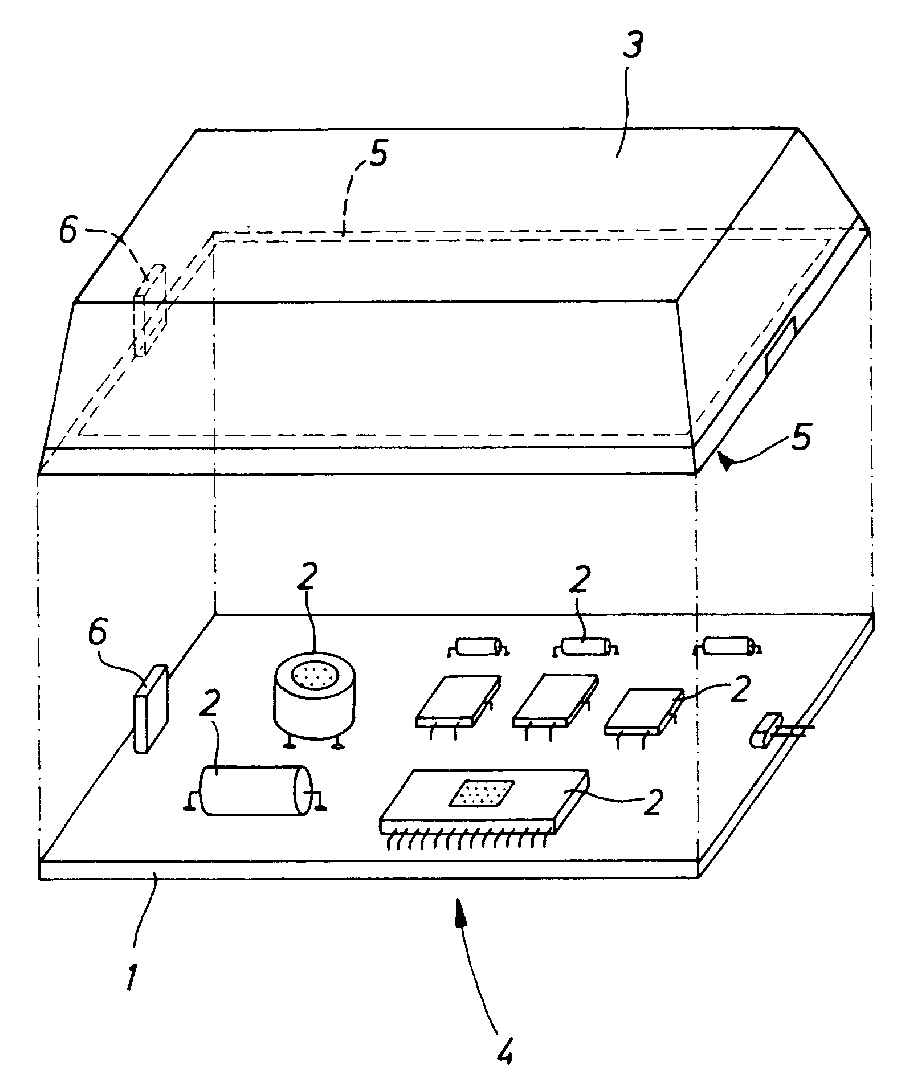
- the carrier plate is a circuit board here 1 has a plurality of electronic components 2, which is attached to the circuit board 1 and electronically are interconnected.
- the circuit board 1 is for example a conventional circuit board electronic circuit.
- the hood 3 is provided for Connect to the circuit board 1, so that protection of the electronic components 2 against external influences, such as Example moisture, dirt or electromagnetic Radiation is provided.
- the electronic components can include brittle, ceramic components (transistors or diodes made of Si / glass, GaAs components, capacitors or Like.), which are susceptible to tension.
- the hood 3 is made of one material e.g.
- the hood 3 can also by others Molding processes known to those skilled in the art, depending on the material.
- the specific material the hood 3 is, for example, a mixed material from a mixture of different plastic materials, which due to their material-physical properties in their mixture a desired thermal Have coefficient of expansion. This will create a elaborate sliding connection between board and hood 3 avoided, as they have so far taken up a lot of time Seal beads have been produced, the tightness is increased and tension build-up is effectively avoided.
- the hood 3 has a chamfer 5 on the inside at its lower edge on that matched to the outer dimension of the circuit board 1 is so that the circuit board 1 is flush with the lower edge of the hood 3 can be inserted into the latter.
- the chamfer 5 serves a better hold and one better bonding or soldering of the hood 3 with the Printed circuit board 1. Furthermore, the printed circuit board 1 on the one hand and the hood 3, on the other hand, each electronic Contacts 6, for electronically conductive connection of the Hood 3 with the circuit board 1 to produce a Shielding the hood 3 against disruptive influences an external, electromagnetic radiation. At the in the embodiment shown in the figure covers the hood 3 the entire circuit board 1 and thus the entirety of electronic components 2 from. However, it is also possible that only a part of the electronic components 2, for example electronic components that one form high-frequency area of the electronic circuit, be covered by a hood to only counter this electromagnetic interference, such as moisture, water, To shield dust or electromagnetic radiation. It is also possible that the hood 3 with the circuit board 1 is not connected electronically, so that the Hood 3 only for sealing against moisture and Dirt or the like is used.
Landscapes
- Engineering & Computer Science (AREA)
- Microelectronics & Electronic Packaging (AREA)
- Shielding Devices Or Components To Electric Or Magnetic Fields (AREA)
- Non-Metallic Protective Coatings For Printed Circuits (AREA)
- Encapsulation Of And Coatings For Semiconductor Or Solid State Devices (AREA)
Abstract
Description
Claims (10)
- Verfahren zur Herstellung einer elektronischen Schaltung (4), insbesondere einer Hochfrequenzschaltung, aufweisend eine Einzahl oder Mehrzahl von elektronischen Baueilen (2), die auf einer Trägerplatte (1) angeordnet und mindestens teilweise mittels einer Haube (3) zum Schutz gegen äußere Einflüsse dicht verschlossen sind, gekennzeichnet durch:a). Herstellen der Haube (3) mittels Spritzgießen aus einem Material, dessen thermischer Ausdehnungskoeffizient auf die abzudeckenden elektronischen Bauteile (2) abgestimmt ist; undb). festes Verbinden der Haube (3) mit der Trägerplatte (1).
- Verfahren nach Anspruch 1, gekennzeichnet durch Verkleben der Haube (3) mit der Trägerplatte (1).
- Verfahren nach Anspruch 1 oder 2, gekennzeichnet durch Verlöten der Haube (3) mit der Trägerplatte (1).
- Verfahren nach einem der vorherigen Ansprüche, gekennzeichnet durch elektrisch leitfähiges Verbinden der Haube (3) mit der Trägerplatte (1) zum Abschirmen der elektronischen Bauteile (2) gegen äußere, elektromagnetisch störende Einflüsse.
- Elektronische Schaltung (4) mit einer Mehrzahl von elektronischen Bauteilen (2), welche auf einer Trägerplatte (1) angeordnet sind, und welche mit einer Haube (3) mindestens teilweise zum Schutz gegen äußere Einflüsse dicht verschlossen sind, dadurch gekennzeichnet, dass die Haube (3) aus einem Material gebildet ist, dessen thermischer Ausdehnungskoeffizient auf die thermische Ausdehnung der abzudeckenden elektronischen Bauteile (2) abgestimmt ist und dass die Haube (3) mit der Trägerplatte (1) fest verbunden ist.
- Elektronische Schaltung (4) nach Anspruch 5, dadurch gekennzeichnet, dass die Haube (3) mit der Trägerplatte (1) durch Klebung oder Lötung fest verbunden ist.
- Elektronische Schaltung (4) nach Anspruch 5 oder 6, dadurch gekennzeichnet, dass die Haube (3) aus einem spezifischen Material entsprechend dem erforderlichen thermischen Ausdehnungskoeffizient der Gesamtheit der elektronischen Bauteile (2) mittels Spritzgießen hergestellt ist.
- Elektronische Schaltung (4) nach einem der vorherigen Ansprüche, dadurch gekennzeichnet, dass die Haube (3) feuchtigkeitsdicht die elektronischen Bauteile (2) verschließt.
- Elektronische Schaltung (4) nach einem der vorherigen Ansprüche, dadurch gekennzeichnet, dass die Haube (3) elektrisch leitend mit der Trägerplatte (1) verbunden ist und geeignet ist zur Abschirmung der Bauteile (2) gegen Störungen durch elektromagnetische Felder.
- Elektronische Schaltung (4) nach Anspruch 9, dadurch gekennzeichnet, dass sie eine hochfrequente Schaltung ist.
Applications Claiming Priority (2)
| Application Number | Priority Date | Filing Date | Title |
|---|---|---|---|
| DE10230304A DE10230304A1 (de) | 2002-07-05 | 2002-07-05 | Verfahren zur Herstellung einer elektronischen Schaltung und elektronische Schaltung |
| DE10230304 | 2002-07-05 |
Publications (2)
| Publication Number | Publication Date |
|---|---|
| EP1378939A2 true EP1378939A2 (de) | 2004-01-07 |
| EP1378939A3 EP1378939A3 (de) | 2008-04-02 |
Family
ID=29719476
Family Applications (1)
| Application Number | Title | Priority Date | Filing Date |
|---|---|---|---|
| EP03010974A Withdrawn EP1378939A3 (de) | 2002-07-05 | 2003-05-16 | Verfahren zur Herstellung einer elektronischen Schaltung und elektronische Schaltung |
Country Status (2)
| Country | Link |
|---|---|
| EP (1) | EP1378939A3 (de) |
| DE (1) | DE10230304A1 (de) |
Family Cites Families (7)
| Publication number | Priority date | Publication date | Assignee | Title |
|---|---|---|---|---|
| JP2616280B2 (ja) * | 1991-04-27 | 1997-06-04 | 株式会社村田製作所 | 発振器及びその製造方法 |
| CH686017A5 (de) * | 1993-04-16 | 1995-11-30 | Microdul Ag | Anordnung mit einem Substrat und mindestens einem Chip. |
| US5566055A (en) * | 1995-03-03 | 1996-10-15 | Parker-Hannifin Corporation | Shieled enclosure for electronics |
| DE19516548A1 (de) * | 1995-05-05 | 1996-11-14 | Blaupunkt Werke Gmbh | Abdeckkappe für elektronisches Bauelement |
| DE19522455A1 (de) * | 1995-06-21 | 1997-01-02 | Telefunken Microelectron | EMV-Abschirmung bei elektronischen Bauelementen |
| WO2001054196A1 (en) * | 2000-01-18 | 2001-07-26 | Sunrisetek, Llc | Dual-sided, surface mountable integrated circuit package |
| DE10026756C2 (de) * | 2000-05-30 | 2002-11-21 | Bosch Gmbh Robert | Elektrische Schaltung |
-
2002
- 2002-07-05 DE DE10230304A patent/DE10230304A1/de not_active Withdrawn
-
2003
- 2003-05-16 EP EP03010974A patent/EP1378939A3/de not_active Withdrawn
Also Published As
| Publication number | Publication date |
|---|---|
| DE10230304A1 (de) | 2004-01-15 |
| EP1378939A3 (de) | 2008-04-02 |
Similar Documents
| Publication | Publication Date | Title |
|---|---|---|
| DE4319965C2 (de) | Verfahren zur Herstellung eines Gehäuses | |
| EP0654962B2 (de) | Abschirmelement und Verfahren zu dessen Herstellung | |
| EP1879294B1 (de) | Elektrisches Gerät und Verfahren zur Herstellung eines elektrischen Geräts | |
| DE102010002765A1 (de) | Gehäusegrundelement eines mehrteiligen Gehäuses und Verfahren zur Montage eines Gehäuses | |
| EP2869674A1 (de) | Elektronikbaugruppe für einen Kraftfahrzeugtürgriff mit einer flexiblen Leiterplatte | |
| WO2008049724A1 (de) | Gehäuse für ein elektronisches steuergerät | |
| EP3016822B1 (de) | Abdichtung für ein gehäuse einer elektronischen schaltungsanordnung, verfahren zum abdichten und getriebesteuerung | |
| EP1762860B1 (de) | Radareinrichtung für ein Kraftfahrzeug und Verfahren zur Herstellung einer Radareinrichtung | |
| DE102013226538B4 (de) | Gehäuse für eine elektronische Schaltungsanordnung und dessen Herstellung | |
| DE202014105530U1 (de) | Steckverbinder | |
| EP3555969A1 (de) | Getriebesteuerungseinrichtung, insbesondere für ein kraftfahrzeug, und verfahren zum herstellen eines steckergehäuses | |
| DE19516936C2 (de) | Verfahren zur Herstellung eines Metallgehäuses mit einer Steckerbuchse | |
| DE102008026771B4 (de) | Geschirmte elektrische Verbindungsanordnung | |
| DE10230304A1 (de) | Verfahren zur Herstellung einer elektronischen Schaltung und elektronische Schaltung | |
| DE102010061714B4 (de) | Elektronikeinheit mit Abschirmung | |
| DE202017101319U1 (de) | Optoelektronikmodul | |
| EP0772959A1 (de) | Wasserdichtes gehäuse mit einer steckverbindung zum schutz von elektronikschaltkreisen | |
| DE102020113700B4 (de) | Piezoelektrisches Funktionsnetzwerk | |
| EP1501341A2 (de) | Anordnung zum Führen von elektrischen Leiterbahnen | |
| DE102012108859B4 (de) | Elektronikmodul | |
| DE4345594B4 (de) | Verfahren zur Herstellung eines eine Abschirmung gegen elektromagnetische Abstrahlung aufweisenden Gehäuses | |
| DE102018220012B4 (de) | Leiterplatte und Verfahren zum Umspritzen einer Leiterplatte | |
| DE102017104893A1 (de) | Optoelektronikmodul | |
| DE19635929A1 (de) | Piezoelektrischer Biegewandler mit einer Trägerschicht | |
| DE102024200873A1 (de) | Elektrische vorrichtung und ihr montageverfahren |
Legal Events
| Date | Code | Title | Description |
|---|---|---|---|
| PUAI | Public reference made under article 153(3) epc to a published international application that has entered the european phase |
Free format text: ORIGINAL CODE: 0009012 |
|
| AK | Designated contracting states |
Kind code of ref document: A2 Designated state(s): AT BE BG CH CY CZ DE DK EE ES FI FR GB GR HU IE IT LI LU MC NL PT RO SE SI SK TR |
|
| AX | Request for extension of the european patent |
Extension state: AL LT LV MK |
|
| RIN1 | Information on inventor provided before grant (corrected) |
Inventor name: PAPZINER, UWE Inventor name: KUENZLER, FRANK Inventor name: WALZ, DIRK Inventor name: BIEHLMANN, BERND |
|
| RIN1 | Information on inventor provided before grant (corrected) |
Inventor name: PAPZINER, UWE Inventor name: KUENZLER, FRANK Inventor name: WALZ, DIRK Inventor name: BIEHLMANN, BERND |
|
| PUAL | Search report despatched |
Free format text: ORIGINAL CODE: 0009013 |
|
| AK | Designated contracting states |
Kind code of ref document: A3 Designated state(s): AT BE BG CH CY CZ DE DK EE ES FI FR GB GR HU IE IT LI LU MC NL PT RO SE SI SK TR |
|
| AX | Request for extension of the european patent |
Extension state: AL LT LV MK |
|
| RIC1 | Information provided on ipc code assigned before grant |
Ipc: H05K 9/00 20060101ALI20080228BHEP Ipc: H01L 23/552 20060101ALI20080228BHEP Ipc: H01L 23/06 20060101AFI20031113BHEP |
|
| AKX | Designation fees paid | ||
| STAA | Information on the status of an ep patent application or granted ep patent |
Free format text: STATUS: THE APPLICATION IS DEEMED TO BE WITHDRAWN |
|
| REG | Reference to a national code |
Ref country code: DE Ref legal event code: 8566 |
|
| 18D | Application deemed to be withdrawn |
Effective date: 20081003 |