EP1376840A2 - Switching power supply circuit and electronic device - Google Patents
Switching power supply circuit and electronic device Download PDFInfo
- Publication number
- EP1376840A2 EP1376840A2 EP03013638A EP03013638A EP1376840A2 EP 1376840 A2 EP1376840 A2 EP 1376840A2 EP 03013638 A EP03013638 A EP 03013638A EP 03013638 A EP03013638 A EP 03013638A EP 1376840 A2 EP1376840 A2 EP 1376840A2
- Authority
- EP
- European Patent Office
- Prior art keywords
- voltage
- circuit
- power supply
- stipulated
- switching
- Prior art date
- Legal status (The legal status is an assumption and is not a legal conclusion. Google has not performed a legal analysis and makes no representation as to the accuracy of the status listed.)
- Withdrawn
Links
Images





Classifications
-
- H—ELECTRICITY
- H02—GENERATION; CONVERSION OR DISTRIBUTION OF ELECTRIC POWER
- H02M—APPARATUS FOR CONVERSION BETWEEN AC AND AC, BETWEEN AC AND DC, OR BETWEEN DC AND DC, AND FOR USE WITH MAINS OR SIMILAR POWER SUPPLY SYSTEMS; CONVERSION OF DC OR AC INPUT POWER INTO SURGE OUTPUT POWER; CONTROL OR REGULATION THEREOF
- H02M3/00—Conversion of DC power input into DC power output
- H02M3/22—Conversion of DC power input into DC power output with intermediate conversion into AC
- H02M3/24—Conversion of DC power input into DC power output with intermediate conversion into AC by static converters
- H02M3/28—Conversion of DC power input into DC power output with intermediate conversion into AC by static converters using discharge tubes with control electrode or semiconductor devices with control electrode to produce the intermediate AC
- H02M3/325—Conversion of DC power input into DC power output with intermediate conversion into AC by static converters using discharge tubes with control electrode or semiconductor devices with control electrode to produce the intermediate AC using devices of a triode or a transistor type requiring continuous application of a control signal
- H02M3/335—Conversion of DC power input into DC power output with intermediate conversion into AC by static converters using discharge tubes with control electrode or semiconductor devices with control electrode to produce the intermediate AC using devices of a triode or a transistor type requiring continuous application of a control signal using semiconductor devices only
- H02M3/33507—Conversion of DC power input into DC power output with intermediate conversion into AC by static converters using discharge tubes with control electrode or semiconductor devices with control electrode to produce the intermediate AC using devices of a triode or a transistor type requiring continuous application of a control signal using semiconductor devices only with automatic control of the output voltage or current, e.g. flyback converters
-
- H—ELECTRICITY
- H02—GENERATION; CONVERSION OR DISTRIBUTION OF ELECTRIC POWER
- H02M—APPARATUS FOR CONVERSION BETWEEN AC AND AC, BETWEEN AC AND DC, OR BETWEEN DC AND DC, AND FOR USE WITH MAINS OR SIMILAR POWER SUPPLY SYSTEMS; CONVERSION OF DC OR AC INPUT POWER INTO SURGE OUTPUT POWER; CONTROL OR REGULATION THEREOF
- H02M1/00—Details of apparatus for conversion
- H02M1/32—Means for protecting converters other than automatic disconnection
-
- H—ELECTRICITY
- H02—GENERATION; CONVERSION OR DISTRIBUTION OF ELECTRIC POWER
- H02M—APPARATUS FOR CONVERSION BETWEEN AC AND AC, BETWEEN AC AND DC, OR BETWEEN DC AND DC, AND FOR USE WITH MAINS OR SIMILAR POWER SUPPLY SYSTEMS; CONVERSION OF DC OR AC INPUT POWER INTO SURGE OUTPUT POWER; CONTROL OR REGULATION THEREOF
- H02M1/00—Details of apparatus for conversion
- H02M1/36—Means for starting or stopping converters
Definitions
- the present invention relates to a switching power supply circuit for converting an AC power supply voltage to a DC power supply voltage, and more particularly to a switching power supply circuit preferably used as a standby power supply circuit and capable of protecting a switching element from a surge voltage.
- Most electronic devices such as television sets, are provided with a main power supply circuit for operating each element in the main unit, and a standby power supply circuit for continuously operating standby circuits, such as a light receiving circuit for receiving a signal from a remote controller, a microcomputer, etc.
- Standby power supply circuits usually have a rectifier circuit connected to an AC power supply, and continuously provide a relatively low power supply voltage (e.g. about 5V) for the above-mentioned light receiving circuit and microcomputer.
- a relatively low power supply voltage e.g. about 5V
- the remote controller has instructed the light receiving circuit to turn on the electronic device
- the main power supply circuit is operated under the control of the microcomputer.
- the remote controller has instructed the light receiving circuit to turn off the device, the operation of the main power supply circuit is stopped under the control of the microcomputer.
- Switching power supply circuits usually comprise a rectifier circuit connected to an AC power supply, a smoothing capacitor for smoothing the output of the rectifier circuit, a converter transformer supplied with a DC current from the smoothing capacitor, and a switching element to which a DC current is supplied from the smoothing capacitor via the primary winding of the transformer.
- the ON/OFF of the switching element is controlled by the output of a switching control circuit. During the OFF period of the switching element, the energy accumulated in the above-mentioned primary winding is transmitted to the secondary winding of the transformer. The voltage generated at the secondary winding is rectified into a DC output voltage.
- the ON/OFF cycle (duty ratio) of the switching element is controlled in accordance with variations in the DC output voltage, thereby stabilizing the DC output voltage of the power supply circuit.
- the capacitance of the smoothing capacitor is usually set small, compared to that of the main power supply. This is to reduce the size of the standby power supply circuit, and also to enhance the responsiveness with which the microcomputer detects whether the supply of power is restored, if it has failed for a short time.
- the smoothing capacitor has a small capacitance, a surge voltage may occur due to the reactance component of the AC power supply line when the AC power supply has been turned on, thereby significantly increasing the voltage across the smoothing capacitor. If the capacitance is large, the capacitor can absorb voltage surges. If, on the other hand, the capacitance is small, the capacitor cannot absorb a surge voltage, with the result that circuits connected to this capacitor may be affected by transient high voltages.
- the switching control circuit incorporated in a switching power supply circuit includes an oscillation circuit, which oscillates when the terminal voltage of the smoothing capacitor exceeds a predetermined value after turn-on of the power supply. If the surge voltage is higher than the breakdown voltage of the switching element, the surge voltage may damage the switching element.
- the microcomputer cannot quickly detect the restoration of power supply if the power supply has failed for a short time. If the main power supply circuit supplies an operation voltage to each element of the main unit before the microcomputer operates, the main unit may malfunction. Further, if a surge absorption element is inserted between the AC power supply and the rectifier circuit, current continuously flows through the surge absorption element, resulting in an increase in power consumption.
- Japanese Patent Application KOKAI Publication No. 2002-51551 discloses a technique for varying the smoothing capacitance of a switching power supply circuit in accordance with the load, such that the smoothing capacitance is reduced in a standby mode, and the ON/OFF of a switching element is controlled only when the input voltage is lower than a predetermined value.
- This publication contains no description concerning protection from a rapid increase in the voltage applied to the smoothing capacitor.
- the invention has been developed in light of the above, and aims to provide a switching power supply circuit with a protection circuit for protecting a switching element from being damaged by a surge voltage when an AC power supply is turned on, and an electronic device using the switching power supply circuit.
- a switching power supply circuit comprising: a direct-current-voltage generating circuit which generates an input direct-current voltage, the direct-current-voltage generating circuit including a rectifier circuit which rectifies an alternating-current power supply voltage, and a smoothing capacitor which smoothes an output from the rectifier circuit; a converter transformer having primary and secondary windings, the input direct-current voltage being applied to an end of the primary winding; a switching element having a main current path and a control electrode, the main current path being connected between another end of the primary winding and a reference potential point, the switching element being turned on/off in response to a switching signal supplied to the control electrode; an output circuit which rectifies a voltage across the secondary winding of the converter transformer, thereby applying an output direct-current voltage to a load; a switching control circuit which has an oscillation circuit, and supplies the switching element with the switching signal on a basis of an oscillation operation of the oscillation circuit; and an oscillation control circuit having a comparator circuit
- the oscillation circuit of the switching control circuit prohibiting the oscillation, thereby protecting the switching element from an excessive surge voltage.
- FIG. 1 is a block diagram illustrating the entire configuration of an electronic device according to the invention, specifically, a power supply system for a television set.
- a power supply switch 11 is a manual switch for turning on/off the supply of an AC power supply voltage of, for example, 100V from a commercial AC power supply.
- power supply switch 11 When the power supply switch 11 has been switched on, power is supplied to a standby power supply circuit 10, thereby applying, for example, 5V to a microcomputer 18 and light receiving circuit 19.
- the standby power supply circuit 10 is a switching power supply.
- the microcomputer 18 is powered by the standby power supply circuit 10.
- the light receiving circuit 19 receives the signal and outputs it to the microcomputer 18, thereby switching on a main power supply switch 12.
- the main power supply circuit 14 When the main power supply switch 12 has been switched on, an AC power supply voltage is applied to a rectifier circuit 13 via the main power supply switch 12.
- the rectifier circuit 13 rectifies the AC power supply voltage into a DC voltage, and outputs it to a main power supply circuit 14.
- the main power supply circuit 14 comprises, for example, a switching power supply circuit.
- the main power supply circuit 14 inputs a DC voltage from the rectifier circuit 13, and applies respective appropriate DC voltages to load circuits, such as a video circuit 15, audio circuit 16, deflection circuit 17, etc.
- the main power supply switch 12 comprises, for example, a relay.
- the main power supply switch 12 When the main power supply switch 12 has been switched off, the supply of power to the rectifier circuit 13 and main power supply circuit 14 is stopped. As a result, the supply of DC the power supply voltages to the load circuits 15, 16 and 17 is also stopped. Even if the operation of the main power supply circuit 14 is stopped, the standby power supply circuit 10 continues to supply power to standby circuits such as the microcomputer 18, light receiving circuit 19, etc. unless the power supply switch 11 is switched off.
- a power ON signal is transmitted to the microcomputer 18 via the light receiving circuit 19.
- the microcomputer 18 switches on a main power supply switch 12, thereby causing the main power supply circuit 14 to re-start the supply of power to the load circuits 15, 16 and 17.
- FIG. 2 is a circuit diagram illustrating the standby power supply circuit 10, according to the first embodiment of the invention, employed in the above-described electronic device.
- the standby power supply circuit 10 comprises an input-side power supply circuit 50 and output-side power supply circuit 60.
- the input-side power supply circuit 50 has a rectifier circuit 10a for rectifying an AC voltage from a commercial power supply (AC input), and a smoothing capacitor 10b for smoothing the output voltage of the rectifier circuit 10a.
- the DC input voltage V IN generated across the smoothing capacitor 10 is applied to an end of the primary winding 31a of a converter transformer 31.
- the other end of the primary winding 31a of the converter transformer 31 is connected to the drain of a MOSFET (hereinafter referred to simply as a "FET") 34 functioning as a switching element.
- the gate of the FET 34 is connected to the GATE terminal of a switching control circuit 32 so that the switching operation of the FET 34 is controlled by the control circuit 32.
- the source terminal of the FET 34 is connected to a reference potential point (earth) as the other end of the smoothing capacitor 10b.
- the drain-source current path of the FET 34 serves as a main current path, and its gate terminal serves as a control input terminal.
- a snubber circuit 37 is connected parallel to the primary winding 31a of the converter transformer 31 to prevent a voltage higher than the drain/source breakdown voltage of the FET 34 from being applied thereto during its switching operation.
- the block 30 indicated by the broken line in FIG. 2 is formed of an IC (Integrated Circuit).
- the FET 34 is incorporated in the IC 30.
- the FET 34 may be provided outside the IC 30.
- the IC 30 further incorporates the previously mentioned switching control circuit 32 and a surge voltage detection circuit 41a.
- the surge voltage detection circuit 41a is provided for interrupting the operation of the switching control circuit 32 to protect the FET 34 when a surge voltage has occurred in the input voltage V IN .
- the switching control circuit 32 generates, at the GATE terminal, an oscillation pulse output for performing switching control on the FET 34.
- the FET 34 is turned on/off, energy is accumulated at the primary winding 31a side of the converter transformer 31 during the OFF period of the FET 34, and energy is discharged to the secondary winding 31b side during the ON period of the FET 34.
- the primary and secondary windings 31a and 31b generate AC voltages V1 and V2 having opposite polarities, respectively.
- the AC voltage V2 is rectified by a diode 36, smoothed by a smoothing capacitor 38, and supplied as a power supply voltage V OUT to the standby circuit incorporating, for example, a microcomputer as a secondary-side load circuit.
- the PTC terminal of the switching control circuit 32 is connected to the output terminal of a photocoupler 39, which is operated by a feedback signal from the output-side power supply circuit 60.
- the photocoupler 39 comprises a light-emitting diode 39a and phototransistor 39b, providing a feedback circuit for supplying a feedback signal from the output-side power supply circuit 60 to the input-side power supply circuit 50.
- the emission diode 39a forms the light emission section of the photocoupler 39
- the phototransistor 39b forms the light receiving section.
- the cathode of the rectifier diode 36 is connected to the anode of the light-emitting diode 39a is connected to the reference potential point via a zener diode 40.
- the collector of the photo transistor 39b is connected to the PTC terminal of the switching control circuit 32, and the emitter of the diode 39b is connected to the reference potential point.
- the output voltage V OUT is higher than a predetermined voltage V T determined by the zener diode 40, the light-emitting diode 39a is turned on.
- the turn-on of the light-emitting diode 39a has been turned on, the light emitted therefrom turns on the phototransistor 39b.
- the voltage at the PTC terminal of the switching control circuit 32 is dropped to LOW, thereby causing the oscillation circuit of the switching control circuit 32 to reduce the output voltage V OUT .
- the output voltage V OUT is controlled to a constant low value by, for example, reducing the oscillation frequency or shortening the switch ON period.
- the output voltage V OUT becomes low, the light-emitting diode 39a is turned off, thereby turning off the phototransistor 39b.
- the voltage at the PTC terminal increases to HIGH, thereby causing the oscillation circuit of the switching control circuit 32 to increase the output voltage V OUT .
- the output voltage V OUT is controlled to a constant high value by, for example, increasing the oscillation frequency or lengthening the switch ON period.
- FIG. 3 is a graph illustrating the relationship between input voltage V IN and the drain voltage V D of a FET.
- the power supply switch 11 is turned on at a time point t0, and the FET 34 starts its switching operation approx. 250 ⁇ s after.
- the input voltage V INO indicated by the broken line expresses the voltage waveform produced when an input AC voltage of 270V has normally increased.
- a surge may occur in the input voltage V INO because of power supply voltage fluctuation, inrush current at the start of power supply, lightning strike, etc. When such a surge has occurred, the input voltage reaches 500V or more as indicated by V INS .
- the voltage V DS indicates the drain voltage of the FET 34 when a surge has occurred in the input voltage V IN .
- the drain voltage V DS reaches 650V or more in a moment of time.
- the drain voltage is much higher than when no surge voltage occurs. This means that an increase in the drain voltage degrades or damages a FET usually used as a standby power supply.
- the embodiment is characterized in that the drain voltage V D of the FET 34 is continuously monitored by the surge voltage detection circuit 41a, and the switching control circuit 32 is controlled on the basis of the monitoring result of the detection circuit 41a. Specifically, when the power supply switch 11 has been turned on (in this state, the standby power supply circuit 10 is not switched on), if the drain voltage V D is higher than a stipulated value, the oscillation circuit of the switching control circuit 32 prohibits or stops oscillation, thereby outputting no pulse train from the GATE terminal, with the result that the FET 34 does not start a switching operation. Thus, the switching control circuit 32 drops, to 0V, the level of the control output signal supplied to the FET 34, thereby prohibiting the operation of the FET 34.
- the surge voltage detection circuit 41a comprises a comparator 35 and stipulated voltage generating section 36.
- the drain voltage V D of the FET 34 is applied to the non-inverting input terminal of the comparator 35, while a stipulated voltage V S from the stipulated voltage generating section 36 is input to the inverting input terminal of the comparator 35.
- the output of the comparator 35 is supplied to the CMP terminal of the switching control circuit 32.
- the drain voltage V D (this is a DC voltage) becomes higher than the stipulated voltage V S , and the output of the comparator 35 becomes HIGH.
- the input DC voltage V IN across the smoothing capacitor 10b is detected upon the supply of power, thereby controlling the switching control circuit 32 so that oscillation is started if the input DC voltage V IN is not higher than a stipulated value, and is prohibited if the voltage V IN is higher than the stipulated value. Accordingly, oscillation is inhibited if the drain voltage V D may exceed the breakdown voltage of the switching element FET 34.
- the detection of the drain voltage V D before the switching element starts oscillation enables the switching element to be protected from an excessive breakdown voltage due to a great increase in the primary smoothing capacitor voltage caused by an increase in the AC input power supply voltage or a surge voltage.
- the above-described configuration may be modified such that a stipulated voltage V S1 is applied to the non-inverting input terminal of the comparator 35, and the input DC voltage V IN is applied to the inverting input terminal of the comparator.
- V S1 a stipulated voltage
- V IN the input DC voltage
- V IN the input DC voltage
- the polarity of the output of the comparator 35 is inverted with respect to that of the previous configuration.
- this will raise no problems if the switching control circuit 32 is modified to respond to the polarity-inverted output.
- FIG. 4 shows a modification of the first embodiment.
- the comparator 35 since the drain voltage VD is input to the comparator 35, the comparator 35 must be a high breakdown voltage comparator, and the stipulated voltage generating section 36 must generate a high voltage.
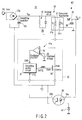
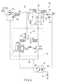
- FIG. 5 shows a surge voltage detection circuit 41c according to a second embodiment of the invention.
- This embodiment is characterized in that the non-inverting input terminal of the comparator 35 is connected to an end of the smoothing capacitor 10a so that the input voltage V IN is input to thereto.
- the stipulated voltage V S is input to the inverting input terminal of the comparator 35 as in the first embodiment.
- a surge voltage is mainly detected during the time ranging from the turn-on of the device to the start of a switching operation by the FET 34.
- the occurrence of a surge voltage may not accurately be detected since the drain voltage V D differs from the input DC voltage V IN .
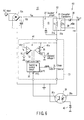
- FIGS. 6 and 7 show voltage detection circuits 44 according to a third embodiment of the invention.
- a low voltage detection circuit 41d is provided as well as the surge voltage detection circuit 41a.
- the low voltage detection circuit 41d comprises a comparator 43 having a non-inverting input terminal to which a voltage V L is input, and an inverting input terminal to which the input DC voltage V IN is input.
- the output of the comparator 35 is connected to a terminal CMP1 of the switching control circuit 32, while the output of the comparator 43 is connected to the other terminal CMP2 of the circuit 32.
- the standby power supply is turned on to thereby turn on the main power supply switch 12.
- the input power supply voltage range for the standby power supply circuit can be easily widened since the output power of the standby power supply circuit is low.
- the input power supply voltage range can deal with input voltages ranging from AC 270V to AC 70V. This AC voltage range corresponds to a DC voltage range of 382V (270* 2 ) - 99V (70* 2 ).
- the input power supply voltage range for the main power supply circuit 14 cannot easily be widened since the output power is high.
- the range is, for example, from AC 270V to AC 170V, i.e., from DC 382V (270* 2 ) to DC 240V (170* 2 ). If a voltage falling out of this range is input to the main power supply circuit 14, the circuit degrades, therefore additional countermeasures are needed.
- the third embodiment is constructed such that the standby power supply circuit 10 performs switching oscillation only when the voltage detection circuit 44 has detected that the input voltage falls within a range of DC 382V - DC 240V. If the switch 12 shown in FIG. 1 is set so that it is turned on when the standby power supply circuit 10 of FIG. 6 is turned on, the main power supply circuit 14 is operated only when the input power supply voltage falls within the range of DC 382V - DC 240V. Thus, the main power supply circuit 14 is prevented from degradation.
- the example shown in FIG. 7 aims to stabilize the detection operation by using one end of the smoothing capacitor 10b as the voltage detecting point.
- FIG. 8 illustrates a surge voltage detection circuit 41f according to a fourth embodiment of the invention.
- a diode 45, resistor R4 and capacitor 46 form a peak hold circuit.
- the comparator 35 compares the voltage held by the peak hold circuit with a third stipulated voltage V S2 generated by a third stipulated voltage generating section 47.
- the surge voltage detection circuit 41f detects whether or not the momentary peak value of the drain voltage V D shown in FIG. 3 is higher than the third stipulated voltage. Accordingly, in this embodiment, the maximum drain voltage of the switching element FET 34, when the standby power supply circuit 10 is performing a switching operation, is detected, in addition to the drain voltage upon turn-on of the electronic device (before oscillation is started). Thus, oscillation is stopped before the maximum drain voltage exceeds the breakdown voltage of the FET 34.
Landscapes
- Engineering & Computer Science (AREA)
- Power Engineering (AREA)
- Dc-Dc Converters (AREA)
Abstract
Description
Claims (9)
- A switching power supply circuit characterized by comprising:a direct-current-voltage generating circuit which generates an input direct-current voltage, the direct-current-voltage generating circuit including a rectifier circuit (10a) which rectifies an alternating-current power supply voltage, and a smoothing capacitor (10b) which smoothes an output from the rectifier circuit (10a);a converter transformer (31) having primary and secondary windings (31a, 31b), the input direct-current voltage being applied to an end of the primary winding;a switching element (34) having a main current path and a control electrode, the main current path being connected between another end of the primary winding (31a) and a reference potential point, the switching element (34) being turned on/off in response to a switching signal supplied to the control electrode;an output circuit (60) which rectifies a voltage generated across the secondary winding (31b) of the converter transformer (31), thereby applying an output direct-current voltage to a load;a switching control circuit (32) which has an oscillation circuit, and supplies the switching element (34) with the switching signal on a basis of an oscillation operation of the oscillation circuit; andan oscillation control circuit (41) having a comparator circuit (35) which compares a first stipulated voltage with the input direct-current voltage applied to the switching element (34), the oscillation control circuit (41) prohibiting an operation of the oscillation circuit of the switching control circuit (32) if the input direct-current voltage is higher than the first stipulated voltage.
- The switching power supply circuit according to claim 1, characterized in that the comparator circuit (35) compares a voltage across the another end of the primary winding (31a) with the first stipulated voltage.
- The switching power supply circuit according to claim 1, characterized in that the comparator circuit (35) compares a voltage across the smoothing capacitor (10b) with the first stipulated voltage.
- The switching power supply circuit according to claim 1, characterized in that the oscillation control circuit (41) includes a voltage dividing circuit (R1-R3, 43) which divides both the input direct-current voltage applied to the switching element (34) and the first stipulated voltage, the comparator circuit (35) comparing division outputs of the voltage dividing circuit.
- The switching power supply circuit according to claim 1, characterized in that the oscillation control circuit (41) includes a peak hold circuit (45, 46, R4) which holds a peak value of the input direct-current voltage applied to the switching element (34), the comparator circuit (35) comparing an output of the peak hold circuit (45, 46, R4, 41) with the first stipulated voltage.
- The switching power supply circuit according to claim 1, characterized in that the oscillation control circuit (41) has a second comparator circuit (43) in addition to the comparator circuit (35), the second comparator circuit (43) comparing the input direct-current voltage applied to the switching element (34), with a second stipulated voltage lower than the first stipulated voltage, the oscillation control circuit (41) prohibiting the operation of the oscillation circuit if the input direct-current voltage is lower than the second stipulated voltage, the oscillation control circuit (41) operating the oscillation circuit if the input direct-current voltage falls within a range from the first stipulated voltage to the second stipulated voltage.
- The switching power supply circuit according to claim 1, characterized by further comprising an output circuit (60) which rectifies a voltage across the secondary winding (31b) of the converter transformer (31), thereby applying an output direct-current voltage to a load, wherein the switching power supply circuit is used as a standby power supply circuit (10) in an electronic device which comprises a main power supply circuit (14), the standby power supply circuit (10), and the load.
- The switching power supply circuit according to claim 7, characterized by further comprising a microcomputer which is supplied with power by the switching power supply circuit.
- The switching power supply circuit according to claim 7, characterized in that the oscillation control circuit (41) has a second comparator circuit (43) in addition to the comparator circuit (35), the second comparator circuit (43) comparing the input direct-current voltage applied to the switching element (34), with a second stipulated voltage lower than the first stipulated voltage, the oscillation control circuit (41) preventing the oscillation circuit from operating if the input direct-current voltage is lower than the second stipulated voltage, the oscillation control circuit (41) operating the oscillation circuit if the input direct-current voltage falls within a range from the first stipulated voltage to the second stipulated voltage.
Applications Claiming Priority (2)
| Application Number | Priority Date | Filing Date | Title |
|---|---|---|---|
| JP2002175612A JP3557198B2 (en) | 2002-06-17 | 2002-06-17 | Switching power supply circuit and electronic equipment |
| JP2002175612 | 2002-06-17 |
Publications (2)
| Publication Number | Publication Date |
|---|---|
| EP1376840A2 true EP1376840A2 (en) | 2004-01-02 |
| EP1376840A3 EP1376840A3 (en) | 2006-03-29 |
Family
ID=29717444
Family Applications (1)
| Application Number | Title | Priority Date | Filing Date |
|---|---|---|---|
| EP03013638A Withdrawn EP1376840A3 (en) | 2002-06-17 | 2003-06-16 | Switching power supply circuit and electronic device |
Country Status (4)
| Country | Link |
|---|---|
| US (1) | US6947296B2 (en) |
| EP (1) | EP1376840A3 (en) |
| JP (1) | JP3557198B2 (en) |
| CN (1) | CN1253997C (en) |
Cited By (1)
| Publication number | Priority date | Publication date | Assignee | Title |
|---|---|---|---|---|
| EP3681026A1 (en) * | 2019-01-14 | 2020-07-15 | Kollmorgen Corporation | Method and apparatus for limiting the output voltages of switch mode power supplies |
Families Citing this family (27)
| Publication number | Priority date | Publication date | Assignee | Title |
|---|---|---|---|---|
| US7082726B2 (en) * | 2003-07-07 | 2006-08-01 | Solatube International, Inc. | Butterfly valve for skylight |
| JP4333485B2 (en) | 2004-06-02 | 2009-09-16 | 船井電機株式会社 | Television apparatus with built-in optical disk device |
| CN100359418C (en) * | 2004-07-05 | 2008-01-02 | 周先谱 | Zero-power-consumption standby power supply control device |
| JP4103862B2 (en) * | 2004-07-26 | 2008-06-18 | オンキヨー株式会社 | Power circuit |
| JP4663371B2 (en) * | 2005-03-31 | 2011-04-06 | 大日本印刷株式会社 | Power supply device |
| WO2006109750A1 (en) * | 2005-04-07 | 2006-10-19 | Nec Corporation | Integrated circuit device evaluation device, evaluation method, and evaluation program |
| DE102005028402A1 (en) * | 2005-06-20 | 2006-12-21 | Austriamicrosystems Ag | Control arrangement for switching configuration has metal oxide semiconductor field effect transistor (MOSFET) having control connection connected to control circuit output |
| CN100452603C (en) * | 2006-01-13 | 2009-01-14 | 四川世纪双虹显示器件有限公司 | Inspecting circuit and method for switching power-supply outputting voltage |
| JP2008118748A (en) * | 2006-11-01 | 2008-05-22 | Denso Corp | Anomaly detection device |
| KR20090065905A (en) * | 2007-12-18 | 2009-06-23 | 삼성전자주식회사 | Power control method of image processing apparatus, image processing system and image processing apparatus |
| TWI356558B (en) | 2008-03-26 | 2012-01-11 | Richtek Technology Corp | Charger control circuit and charger control method |
| CN101546914B (en) * | 2008-03-27 | 2012-12-26 | 立锜科技股份有限公司 | Charger control circuit and charger control method |
| JP5116732B2 (en) | 2009-07-02 | 2013-01-09 | ローム株式会社 | Power supply control device, power supply system, and electronic device |
| JP5358338B2 (en) * | 2009-08-06 | 2013-12-04 | セミコンダクター・コンポーネンツ・インダストリーズ・リミテッド・ライアビリティ・カンパニー | Remote control signal receiving circuit |
| JP2011082745A (en) * | 2009-10-06 | 2011-04-21 | Sanyo Electric Co Ltd | Microcomputer |
| KR20110051862A (en) * | 2009-11-11 | 2011-05-18 | 삼성전자주식회사 | Network communication device and method through HDMD in standby mode |
| US20120287689A1 (en) * | 2009-12-28 | 2012-11-15 | William Vincent Fitzgerald | Synchronous rectifier disabling arrangement |
| JP5476212B2 (en) * | 2010-05-25 | 2014-04-23 | パナソニック株式会社 | POWER SUPPLY DEVICE AND LIGHTING DEVICE USING THE SAME |
| JP2012125090A (en) * | 2010-12-10 | 2012-06-28 | Hitachi Media Electoronics Co Ltd | Switching power supply and display device with it |
| CN202995349U (en) * | 2012-12-26 | 2013-06-12 | 黄冠雄 | Micro-power-consumption standby system and thick film hybrid integrated circuit module |
| WO2014203487A1 (en) | 2013-06-20 | 2014-12-24 | 富士電機株式会社 | Semiconductor device, control ic for switching power supply, and switching power supply device |
| US20170324270A1 (en) * | 2013-12-26 | 2017-11-09 | Calvin Shie-Ning Wang | Standby circuit, and outlet, plug, and device having the same |
| WO2017133383A1 (en) | 2016-02-05 | 2017-08-10 | 广东欧珀移动通信有限公司 | Adapter and charge control method |
| CN109643955B (en) | 2016-08-30 | 2021-03-12 | 新唐科技日本株式会社 | Switching power supply device and semiconductor device |
| US11239776B2 (en) * | 2019-02-11 | 2022-02-01 | Regal Beloit America, Inc. | Motor controller having low standby power consumption |
| US11168480B2 (en) | 2019-02-21 | 2021-11-09 | Solatube International, Inc. | Skylight dimmer |
| US11277024B2 (en) | 2020-07-24 | 2022-03-15 | ZQ Power, LLC | Devices, systems, and methods for reducing standby power consumption |
Family Cites Families (12)
| Publication number | Priority date | Publication date | Assignee | Title |
|---|---|---|---|---|
| JP2893720B2 (en) | 1989-05-31 | 1999-05-24 | ソニー株式会社 | Method for manufacturing optical information recording medium |
| US5289046A (en) * | 1992-06-10 | 1994-02-22 | Digital Equipment Corporation | Power converter with controller for switching between primary and battery power sources |
| JPH08182315A (en) | 1994-12-27 | 1996-07-12 | Oki Electric Ind Co Ltd | Switching power source |
| US5754414A (en) * | 1996-02-23 | 1998-05-19 | Hanington; Gary J. | Self-compensating switching power converter |
| JP2900876B2 (en) * | 1996-03-19 | 1999-06-02 | サンケン電気株式会社 | Display power supply |
| US5999421A (en) * | 1999-03-31 | 1999-12-07 | Liu; Kwang H. | Dual-channel power system with an eight-pin PWM control chip |
| US6462971B1 (en) * | 1999-09-24 | 2002-10-08 | Power Integrations, Inc. | Method and apparatus providing a multi-function terminal for a power supply controller |
| JP2001218466A (en) * | 2000-02-03 | 2001-08-10 | Sony Corp | High voltage stabilization circuit |
| JP4072664B2 (en) | 2000-04-12 | 2008-04-09 | ソニー株式会社 | Electronic equipment power supply |
| TW521481B (en) * | 2000-05-17 | 2003-02-21 | Sony Corp | Switching power supply apparatus with active clamp circuit |
| JP3703378B2 (en) | 2000-08-02 | 2005-10-05 | 松下電器産業株式会社 | Switching power supply |
| JP3412624B2 (en) * | 2001-06-08 | 2003-06-03 | サンケン電気株式会社 | Switching power supply |
-
2002
- 2002-06-17 JP JP2002175612A patent/JP3557198B2/en not_active Expired - Fee Related
-
2003
- 2003-06-16 EP EP03013638A patent/EP1376840A3/en not_active Withdrawn
- 2003-06-17 CN CN03143050.3A patent/CN1253997C/en not_active Expired - Fee Related
- 2003-06-17 US US10/462,828 patent/US6947296B2/en not_active Expired - Fee Related
Cited By (1)
| Publication number | Priority date | Publication date | Assignee | Title |
|---|---|---|---|---|
| EP3681026A1 (en) * | 2019-01-14 | 2020-07-15 | Kollmorgen Corporation | Method and apparatus for limiting the output voltages of switch mode power supplies |
Also Published As
| Publication number | Publication date |
|---|---|
| JP2004023894A (en) | 2004-01-22 |
| EP1376840A3 (en) | 2006-03-29 |
| JP3557198B2 (en) | 2004-08-25 |
| US20040052092A1 (en) | 2004-03-18 |
| CN1253997C (en) | 2006-04-26 |
| US6947296B2 (en) | 2005-09-20 |
| CN1471224A (en) | 2004-01-28 |
Similar Documents
| Publication | Publication Date | Title |
|---|---|---|
| US6947296B2 (en) | Switching power supply circuit and electronic device | |
| US6480043B2 (en) | Circuit and method for protecting a switching power supply from a fault condition | |
| US7339804B2 (en) | DC-DC converter | |
| US7375987B2 (en) | Resonant switching power source apparatus | |
| US7649755B2 (en) | Switched mode power supply with soft start operation | |
| US10199942B2 (en) | Controller and power supply | |
| US6385060B1 (en) | Switching power supply with reduced energy transfer during a fault condition | |
| US8054600B2 (en) | Switching power supply device | |
| KR100296635B1 (en) | Smps having low voltage protection circuit | |
| US20120014145A1 (en) | Startup circuit | |
| US7295450B2 (en) | Primary-controlled SMPS with adjustable switching frequency for output voltage and current control | |
| US6816392B2 (en) | Overcurrent output protecting circuit and constant-voltage switching power supply incorporating the same | |
| US11703550B2 (en) | Resonance voltage attenuation detection circuit, semiconductor device for switching power, and switching power supply | |
| US8283909B2 (en) | Switching mode power supply apparatus and power supply method thereof | |
| US8179172B2 (en) | Auto-restart circuit and auto-restart method | |
| JP4557110B2 (en) | Switching power supply | |
| JP2019176612A (en) | Switching power supply | |
| JPH07163142A (en) | Switching power supply | |
| JP3097403U (en) | Switching power supply | |
| JPH09168100A (en) | Power supply for television | |
| JPH09238474A (en) | Power supply device, discharge lamp lighting device and lighting equipment | |
| JP2011035987A (en) | Switching power supply unit | |
| KR19980022751U (en) | Inrush Current Prevention Circuit in Monitor Power Supply Circuit | |
| JPH04344169A (en) | Power unit | |
| KR19980066949A (en) | Overvoltage input protection circuit of power supply |
Legal Events
| Date | Code | Title | Description |
|---|---|---|---|
| PUAI | Public reference made under article 153(3) epc to a published international application that has entered the european phase |
Free format text: ORIGINAL CODE: 0009012 |
|
| 17P | Request for examination filed |
Effective date: 20030616 |
|
| AK | Designated contracting states |
Kind code of ref document: A2 Designated state(s): AT BE BG CH CY CZ DE DK EE ES FI FR GB GR HU IE IT LI LU MC NL PT RO SE SI SK TR |
|
| AX | Request for extension of the european patent |
Extension state: AL LT LV MK |
|
| PUAL | Search report despatched |
Free format text: ORIGINAL CODE: 0009013 |
|
| AK | Designated contracting states |
Kind code of ref document: A3 Designated state(s): AT BE BG CH CY CZ DE DK EE ES FI FR GB GR HU IE IT LI LU MC NL PT RO SE SI SK TR |
|
| AX | Request for extension of the european patent |
Extension state: AL LT LV MK |
|
| AKX | Designation fees paid |
Designated state(s): DE FR GB |
|
| STAA | Information on the status of an ep patent application or granted ep patent |
Free format text: STATUS: THE APPLICATION HAS BEEN WITHDRAWN |
|
| 18W | Application withdrawn |
Effective date: 20090306 |