EP1376702A1 - Gate and cmos structure and mos structure - Google Patents
Gate and cmos structure and mos structure Download PDFInfo
- Publication number
- EP1376702A1 EP1376702A1 EP02705064A EP02705064A EP1376702A1 EP 1376702 A1 EP1376702 A1 EP 1376702A1 EP 02705064 A EP02705064 A EP 02705064A EP 02705064 A EP02705064 A EP 02705064A EP 1376702 A1 EP1376702 A1 EP 1376702A1
- Authority
- EP
- European Patent Office
- Prior art keywords
- gate
- intermetallic compound
- semiconductor
- compound semiconductor
- metal
- Prior art date
- Legal status (The legal status is an assumption and is not a legal conclusion. Google has not performed a legal analysis and makes no representation as to the accuracy of the status listed.)
- Withdrawn
Links
Images



Classifications
-
- H—ELECTRICITY
- H10—SEMICONDUCTOR DEVICES; ELECTRIC SOLID-STATE DEVICES NOT OTHERWISE PROVIDED FOR
- H10D—INORGANIC ELECTRIC SEMICONDUCTOR DEVICES
- H10D30/00—Field-effect transistors [FET]
- H10D30/60—Insulated-gate field-effect transistors [IGFET]
-
- H—ELECTRICITY
- H10—SEMICONDUCTOR DEVICES; ELECTRIC SOLID-STATE DEVICES NOT OTHERWISE PROVIDED FOR
- H10D—INORGANIC ELECTRIC SEMICONDUCTOR DEVICES
- H10D64/00—Electrodes of devices having potential barriers
- H10D64/01—Manufacture or treatment
- H10D64/013—Manufacture or treatment of electrodes having a conductor capacitively coupled to a semiconductor by an insulator
- H10D64/01302—Manufacture or treatment of electrodes having a conductor capacitively coupled to a semiconductor by an insulator the insulator being formed after the semiconductor body, the semiconductor being silicon
- H10D64/01304—Manufacture or treatment of electrodes having a conductor capacitively coupled to a semiconductor by an insulator the insulator being formed after the semiconductor body, the semiconductor being silicon characterised by the conductor
- H10D64/01306—Manufacture or treatment of electrodes having a conductor capacitively coupled to a semiconductor by an insulator the insulator being formed after the semiconductor body, the semiconductor being silicon characterised by the conductor the conductor comprising a layer of silicon contacting the insulator, e.g. polysilicon
- H10D64/01308—Manufacture or treatment of electrodes having a conductor capacitively coupled to a semiconductor by an insulator the insulator being formed after the semiconductor body, the semiconductor being silicon characterised by the conductor the conductor comprising a layer of silicon contacting the insulator, e.g. polysilicon the conductor further comprising a non-elemental silicon additional conductive layer, e.g. a metal silicide layer formed by the reaction of silicon with an implanted metal
-
- H—ELECTRICITY
- H10—SEMICONDUCTOR DEVICES; ELECTRIC SOLID-STATE DEVICES NOT OTHERWISE PROVIDED FOR
- H10D—INORGANIC ELECTRIC SEMICONDUCTOR DEVICES
- H10D64/00—Electrodes of devices having potential barriers
- H10D64/60—Electrodes characterised by their materials
- H10D64/66—Electrodes having a conductor capacitively coupled to a semiconductor by an insulator, e.g. MIS electrodes
- H10D64/661—Electrodes having a conductor capacitively coupled to a semiconductor by an insulator, e.g. MIS electrodes the conductor comprising a layer of silicon contacting the insulator, e.g. polysilicon having vertical doping variation
- H10D64/662—Electrodes having a conductor capacitively coupled to a semiconductor by an insulator, e.g. MIS electrodes the conductor comprising a layer of silicon contacting the insulator, e.g. polysilicon having vertical doping variation the conductor further comprising additional layers, e.g. multiple silicon layers having different crystal structures
- H10D64/663—Electrodes having a conductor capacitively coupled to a semiconductor by an insulator, e.g. MIS electrodes the conductor comprising a layer of silicon contacting the insulator, e.g. polysilicon having vertical doping variation the conductor further comprising additional layers, e.g. multiple silicon layers having different crystal structures the additional layers comprising a silicide layer contacting the layer of silicon, e.g. polycide gates
-
- H—ELECTRICITY
- H10—SEMICONDUCTOR DEVICES; ELECTRIC SOLID-STATE DEVICES NOT OTHERWISE PROVIDED FOR
- H10D—INORGANIC ELECTRIC SEMICONDUCTOR DEVICES
- H10D84/00—Integrated devices formed in or on semiconductor substrates that comprise only semiconducting layers, e.g. on Si wafers or on GaAs-on-Si wafers
- H10D84/01—Manufacture or treatment
- H10D84/0123—Integrating together multiple components covered by H10D12/00 or H10D30/00, e.g. integrating multiple IGBTs
- H10D84/0126—Integrating together multiple components covered by H10D12/00 or H10D30/00, e.g. integrating multiple IGBTs the components including insulated gates, e.g. IGFETs
- H10D84/0165—Integrating together multiple components covered by H10D12/00 or H10D30/00, e.g. integrating multiple IGBTs the components including insulated gates, e.g. IGFETs the components including complementary IGFETs, e.g. CMOS devices
- H10D84/0172—Manufacturing their gate conductors
-
- H—ELECTRICITY
- H10—SEMICONDUCTOR DEVICES; ELECTRIC SOLID-STATE DEVICES NOT OTHERWISE PROVIDED FOR
- H10D—INORGANIC ELECTRIC SEMICONDUCTOR DEVICES
- H10D84/00—Integrated devices formed in or on semiconductor substrates that comprise only semiconducting layers, e.g. on Si wafers or on GaAs-on-Si wafers
- H10D84/01—Manufacture or treatment
- H10D84/0123—Integrating together multiple components covered by H10D12/00 or H10D30/00, e.g. integrating multiple IGBTs
- H10D84/0126—Integrating together multiple components covered by H10D12/00 or H10D30/00, e.g. integrating multiple IGBTs the components including insulated gates, e.g. IGFETs
- H10D84/0165—Integrating together multiple components covered by H10D12/00 or H10D30/00, e.g. integrating multiple IGBTs the components including insulated gates, e.g. IGFETs the components including complementary IGFETs, e.g. CMOS devices
- H10D84/0172—Manufacturing their gate conductors
- H10D84/0177—Manufacturing their gate conductors the gate conductors having different materials or different implants
-
- H—ELECTRICITY
- H10—SEMICONDUCTOR DEVICES; ELECTRIC SOLID-STATE DEVICES NOT OTHERWISE PROVIDED FOR
- H10D—INORGANIC ELECTRIC SEMICONDUCTOR DEVICES
- H10D84/00—Integrated devices formed in or on semiconductor substrates that comprise only semiconducting layers, e.g. on Si wafers or on GaAs-on-Si wafers
- H10D84/01—Manufacture or treatment
- H10D84/02—Manufacture or treatment characterised by using material-based technologies
- H10D84/03—Manufacture or treatment characterised by using material-based technologies using Group IV technology, e.g. silicon technology or silicon-carbide [SiC] technology
- H10D84/038—Manufacture or treatment characterised by using material-based technologies using Group IV technology, e.g. silicon technology or silicon-carbide [SiC] technology using silicon technology, e.g. SiGe
-
- H—ELECTRICITY
- H10—SEMICONDUCTOR DEVICES; ELECTRIC SOLID-STATE DEVICES NOT OTHERWISE PROVIDED FOR
- H10D—INORGANIC ELECTRIC SEMICONDUCTOR DEVICES
- H10D84/00—Integrated devices formed in or on semiconductor substrates that comprise only semiconducting layers, e.g. on Si wafers or on GaAs-on-Si wafers
- H10D84/80—Integrated devices formed in or on semiconductor substrates that comprise only semiconducting layers, e.g. on Si wafers or on GaAs-on-Si wafers characterised by the integration of at least one component covered by groups H10D12/00 or H10D30/00, e.g. integration of IGFETs
- H10D84/82—Integrated devices formed in or on semiconductor substrates that comprise only semiconducting layers, e.g. on Si wafers or on GaAs-on-Si wafers characterised by the integration of at least one component covered by groups H10D12/00 or H10D30/00, e.g. integration of IGFETs of only field-effect components
- H10D84/83—Integrated devices formed in or on semiconductor substrates that comprise only semiconducting layers, e.g. on Si wafers or on GaAs-on-Si wafers characterised by the integration of at least one component covered by groups H10D12/00 or H10D30/00, e.g. integration of IGFETs of only field-effect components of only insulated-gate FETs [IGFET]
- H10D84/85—Complementary IGFETs, e.g. CMOS
Definitions
- the invention of this application relates to a gate, CMOS structure, and MOSstructure. More particularly, theinvention of this application concerns a novel gate that replaces a conventional gate and that is useful for a next-generation integrated circuit, and a novel CMOS structure and MOS structure each of that uses that gate.
- CMOS Complementary Metal Oxide Semiconductor
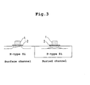
- a field effect transistor (FET) of a conventional CMOS structure uses a silicon oxide film of SiO 2 as a gate insulative film (2) and has its gate constructed of a gate (1) that uses polycrystalline silicon (polysilicon) made to contain an n-type impurity therein.
- the threshold value voltage Vth that is a voltage that allows a bias voltage to be applied to the gate (1) to thereby start causing the flow of a channel-opening current is determined depending basically upon the Fermi level of a substrate Si and that of the gate material. For this reason, in the CMOS structure, the threshold voltage Vth differs between the n-type substrate and a p-type substrate.
- the Vth is conventionally controlled by performing ion-implantation of impurities into either channel region.
- one channel is a surface channel and the other one is a buried channel.
- the position of the Fermi level can be controlled over a wide range by changing the impurity concentration therein and, accordingly, the Vth can be freely set and controlled also with respect to the electric conductivity (p, n) of the substrate.
- the conventional CMOS structure as described above has the following problems when trying to further increase the integrated version level of the integrated circuit.
- the metal silicide (3) which is an intermetallic compound having an electric conductivity substantially the same as that of metal has been found out as being usable.
- the metal silicide (3) which is an intermetallic compound having an electric conductivity substantially the same as that of metal has been found out as being usable.
- the invention of this application has been made in view of the existing circumstances mentioned above and has an object to provide a novel gate that can solve the points in problem inherent in the prior art, that can realize the decrease in resistance to such an extent as not in the prior art, and that can greatly contribute to further increasing the integrated version level of the integrated circuit, and a novel CMOS structure and MOS structure each of that uses such gate.
- the invention of this application provides a gate (first aspect) comprising an intermetallic compound semiconductor that has an electric conductivity in a range of no less than 10 2 S ⁇ m -1 , nor more than 10 5 S ⁇ m -1 without impurities and that has a semiconductor band structure. Also, the invention of this application provides a gate (second aspect) wherein, impurities are added to the said intermetallic compound semiconductor.
- the invention of this application also provides a gate wherein, in the above-described gate, the intermetallic compound semiconductor is a compound of a metal and a IV-group element (third aspect) or wherein, in the above-described gate, any of C, Si, and Ge is used as the IV-group element (fourth aspect) .
- the invention of this application also provides a gate wherein, in the above-described gate (fifth aspect), any one intermetallic compound semiconductor of CrSi 2 , MnSi 2 , MoSi 2 , Ru 2 Si 3 , WSi 2 , ReSi 1.75-2 , OsSi, OS 2 Si 3 , OsSi 2 , FeSi 2 , IrSi 2 , BaSi 2 , CaSi 2 and Mg 2 Si is used.
- the invention of this invention also provides a CMOS structure that uses the above-described gate (sixth aspect), or a MOS structure that uses the above-described gate (seventh aspect).
- the invention of this application has been achieved based on the completely new knowledge procured by the inventors of the invention of this application that as the material for the gate there is used an an intermetallic compound semiconductor i . e. one having an electric conductivity in a range of no less than 10 2 S ⁇ m -1 , nor more than 10 5 S ⁇ m -1 without impurities and also having a semiconductor band structure.
- an intermetallic compound semiconductor i . e. one having an electric conductivity in a range of no less than 10 2 S ⁇ m -1 , nor more than 10 5 S ⁇ m -1 without impurities and also having a semiconductor band structure.
- this intermetallic compound semiconductor (1) has an electric conductivity in a range of no less than 10 2 S ⁇ m -1 , nor more than 10 5 S ⁇ m -1 without impurities, (2) has a semiconductor band structure, and (3) is a semiconductor compound that is comprised of metal and a semiconductor.
- the intermetallic compound semiconductor has an electric conductivity in a range of no less than 10 2 S ⁇ m -1 , nor more than 10 5 S ⁇ m -1 without impurities.
- the electric conductivity of a semiconductor in general is in a range of from 10 -2 to 10 4 S ⁇ m -1 at normal temperature, whereas an electric conductivity of metal in general is in a range of from 10 6 to 10 8 S ⁇ m -1 at normal temperature.
- An intermetallic compound semiconductor, which is used for a gate material of the invention of this application has a electric conductivity closed to an electric conductivity of metal compare to a semiconductor in general. Also, the electric conductivity of the intermetallic compound semiconductor can be improved by adding impurities.
- the wording "a semiconductor band structure" means that the intermetallic compound semiconductor has an electric-conduction mechanism that enables freely controlling the Fermi level. As a result of this, it becomes possible to control the threshold voltage Vth, whereby it becomes possible to realize a gate for use for n type on the n-type substrate and a gate for use for p type on the p-type substrate. Namely, owing to this property, the intermetallic compound semiconductor becomes able to be used as the material for use for gate.
- the semiconductor compound of metal and a semiconductor that canbe the material having the above-described two properties there is a compound of metal and an element of the IV group. More specifically, there can be taken up as examples thereof the compounds of metals and silicon such as CrSi 2 , MnSi 2 , MoSi 2 , Ru 2 Si 3 , WSi 2 , ReSi 1.75-2 , OsSi, Os 2 Si 3 , OsSi 2 , FeSi 2 , IrSi 2 , BaSi 2 , CaSi 2 , Mg 2 Sior the compounds the compositions of that each are in the neighborhood of that of those compounds.
- the compounds in this case can be called "semiconductor silicides".
- compounds of metal and C or Ge there can be also taken up as such examples compounds of metal and C or Ge.
- compounds of metal and Si and C or Ge can also be said material.
- pn control becomes possible by doping Co and Cr.
- the gate according to the invention of this application thatconsistsoftheintermetallic compoundsemiconductor having the above-described properties not only has excellent low resistance but also enables realizing easy control.
- the freedom in which the CMOS structure can be designed is thereby greatly widened.
- both of the np channels become surface channels, it is also possible to avoid having the short-channel effect.
- the ion-implantation of impurities that needed to be so far performed becomes unnecessary, whereby the property of the channel region being crystalline can also be ensured.
- CMOS structure that is simple and that has excellent controllability of process.
- the gate according to the invention of this application can needless to say be applied also to the MOS structure. Excellent effects that are as in the case of the CMOS structure are realized.
- Fig. 1 illustrates a CMOS structure that uses a gate according to an embodiment of the invention of this application.
- any one intermetallic compound semiconductor of CrSi 2 , MnSi 2 , MoSi 2 , Ru 2 Si 3 , WSi 2 , ReSi 1.75-2 , OsSi, OS 2 Si 3 , OsSi 2 , FeSi 2 , IrSi 2 , BaSi 2 , CaSi 2 and Mg 2 Si is used for the gate material.
- CMOS structure by controlling a pn conduction mechanism of the intermetallic compound semiconductor, a gate (10) for use for n type is provided on an n-type substrate and a gate (11) for use for p-type is provided on a p-type substrate.
- the illustrated CMOS structure does not have the short-channel effect which conventionally occurred in the buried channel in the CMOS structure. Resultantly, the illustrated CMOS structure provides a gate and CMOS structure that are again better for conversion into an integrated version.
- Fig. 2 shows a graph of light absorption spectrum of IrSi 2 as an embodiment of above-described intermetallic compound semiconductor.
- the vertical axis in Fig. 2 shows spectral intensity and the horizontal axis in Fig. 2 shows wavelength.
- the band gap of IrSi 2 is 1.13 eV because of there is spectral absorption around 1100 nm wavelength. That is, it shows that the IrSi 2 has a semiconductor band structure.
Landscapes
- Metal-Oxide And Bipolar Metal-Oxide Semiconductor Integrated Circuits (AREA)
- Electrodes Of Semiconductors (AREA)
- Insulated Gate Type Field-Effect Transistor (AREA)
Abstract
Provided are a novel gate, a CMOS structure, and a MOS
structure each of that has low resistance and excellent
controllability. The gate is comprised of an intermetallic
compound semiconductor that has an electric conductivity in a
range of no less than 102 S·m-1, nor more than 105 S·m-1 without
impurities and has a band structure like that of a semiconductor.
Description
The invention of this application relates to a gate, CMOS
structure, and MOSstructure. More particularly, theinvention
of this application concerns a novel gate that replaces a
conventional gate and that is useful for a next-generation
integrated circuit, and a novel CMOS structure and MOS structure
each of that uses that gate.
The requirements that are demanded regarding the
next-generation integrated circuits are (1) the increase in the
integrated level, (2) the increase in the speed, and (3) the
decrease in the power consumption. As a structure that satisfies
these requirements, a Complementary Metal Oxide Semiconductor
(CMOS) structure is known.
For example, as illustrated in Fig. 3, a field effect
transistor (FET) of a conventional CMOS structure uses a silicon
oxide film of SiO2 as a gate insulative film (2) and has its
gate constructed of a gate (1) that uses polycrystalline silicon
(polysilicon) made to contain an n-type impurity therein.
Ordinarily, the threshold value voltage Vth that is a
voltage that allows a bias voltage to be applied to the gate
(1) to thereby start causing the flow of a channel-opening current
is determined depending basically upon the Fermi level of a
substrate Si and that of the gate material. For this reason,
in the CMOS structure, the threshold voltage Vth differs between
the n-type substrate and a p-type substrate.
On this account, because for making the CMOS operation
stable it is necessary to make the both threshold voltages Vth
substantially the same in level, the Vth is conventionally
controlled by performing ion-implantation of impurities into
either channel region.
In this case, as illustrated, one channel is a surface
channel and the other one is a buried channel. And, in case
of the polycrystalline Si that is a semiconductor, the position
of the Fermi level can be controlled over a wide range by changing
the impurity concentration therein and, accordingly, the Vth
can be freely set and controlled also with respect to the electric
conductivity (p, n) of the substrate.
However, the conventional CMOS structure as described
above has the following problems when trying to further increase
the integrated version level of the integrated circuit.
Namely, the demand for the micronizing of the gate wire
width that is important for high integration has more and more
increased, and therefore it is necessary to prevent the increase
in the resistance following such micronization. However, as
described above, in the case of the polycrystalline Si gate (1)
made by doping the polycrystalline Si with impurities, a limit
has started to be imposed upon the suppression of the resistance.
In order to solve this problem, constructing the gate (1)
using metal has been proposed, and as a result, the using of
a high-melting point metal such as tungsten has nowadays been
studied and examined. However, in case of a metal gate, it is
pointed out that the following problems come up. Namely, (a)
because the Vth is determined in accordance with the work function
of the Fermi level of the backing Si and the metal, the range
of control of the Fermi level that had theretofore been freely
set becomes narrow, with the result that the problem that the
Vth becomes difficult to control arises. (b) The adherences
between the metal and gate insulative films such as SiO2 are
bad. (c) Owing to the diffusion of the metal there increases
the leak current of the gate insulative film. (d) The metal
becomes diffused up to the channel region, whereby trap of the
carriers occurs. And so forth.
Also, recently, the metal silicide (3) which is an
intermetallic compound having an electric conductivity
substantially the same as that of metal has been found out as
being usable. Thereby, providing it on the polycrystalline Si
gate (1) as illustrated in Fig. 4 has been proposed with an aim
to decrease the gate resistance even to a small extent. However,
even in this case, although the above-described problems such
as those following the use of metal do not exist, because the
metal silicide (3) is merely provided on the gate (1), it doesn't
happen that the resistance of the gate (1) itself will decrease.
Therefore, realizing the remarkable decrease in the resistance
is not expected.
The invention of this application has been made in view
of the existing circumstances mentioned above and has an object
to provide a novel gate that can solve the points in problem
inherent in the prior art, that can realize the decrease in
resistance to such an extent as not in the prior art, and that
can greatly contribute to further increasing the integrated
version level of the integrated circuit, and a novel CMOS
structure and MOS structure each of that uses such gate.
To attain the above object, the invention of this
application provides a gate (first aspect) comprising an
intermetallic compound semiconductor that has an electric
conductivity in a range of no less than 102 S·m-1, nor more than
105 S·m-1 without impurities and that has a semiconductor band
structure. Also, the invention of this application provides
a gate (second aspect) wherein, impurities are added to the said
intermetallic compound semiconductor.
Also, the invention of this application also provides a
gate wherein, in the above-described gate, the intermetallic
compound semiconductor is a compound of a metal and a IV-group
element (third aspect) or wherein, in the above-described gate,
any of C, Si, and Ge is used as the IV-group element (fourth
aspect) .
The invention of this application also provides a gate
wherein, in the above-described gate (fifth aspect), any one
intermetallic compound semiconductor of CrSi2, MnSi2, MoSi2,
Ru2Si3, WSi2, ReSi1.75-2, OsSi, OS2Si3, OsSi2, FeSi2, IrSi2, BaSi2,
CaSi2 and Mg2Si is used.
Further, the invention of this invention also provides
a CMOS structure that uses the above-described gate (sixth
aspect), or a MOS structure that uses the above-described gate
(seventh aspect).
Here, reference numerals in the drawings designate as
follows:
The invention of this application has been achieved based
on the completely new knowledge procured by the inventors of
the invention of this application that as the material for the
gate there is used an an intermetallic compound semiconductor
i . e. one having an electric conductivity in a range of no less
than 102 S·m-1, nor more than 105 S·m-1 without impurities and
also having a semiconductor band structure. As a result of this,
the invention of this application can be a basic technique that
enables realizing further decrease in the resistance and that
therefore is indispensable to the integrated circuit of the next
generation and the next, but that next, generation.
More specifically, this intermetallic compound
semiconductor (1) has an electric conductivity in a range of
no less than 102 S·m-1, nor more than 105 S·m-1 without impurities,
(2) has a semiconductor band structure, and (3) is a semiconductor
compound that is comprised of metal and a semiconductor.
First, (1) that the intermetallic compound semiconductor
has an electric conductivity in a range of no less than 102 S·
m-1, nor more than 105 S·m-1 without impurities. The electric
conductivity of a semiconductor in general is in a range of from
10-2 to 104 S·m-1 at normal temperature, whereas an electric
conductivity of metal in general is in a range of from 106 to
108 S·m-1 at normal temperature. An intermetallic compound
semiconductor, which is used for a gate material of the invention
of this application, has a electric conductivity closed to an
electric conductivity of metal compare to a semiconductor in
general. Also, the electric conductivity of the intermetallic
compound semiconductor can be improved by adding impurities.
Next, (2) the wording "a semiconductor band structure"
means that the intermetallic compound semiconductor has an
electric-conduction mechanism that enables freely controlling
the Fermi level. As a result of this, it becomes possible to
control the threshold voltage Vth, whereby it becomes possible
to realize a gate for use for n type on the n-type substrate
and a gate for use for p type on the p-type substrate. Namely,
owing to this property, the intermetallic compound semiconductor
becomes able to be used as the material for use for gate.
(3) Regarding the semiconductor compound of metal and a
semiconductor that canbe the material having the above-described
two properties, for example, there is a compound of metal and
an element of the IV group. More specifically, there can be
taken up as examples thereof the compounds of metals and silicon
such as CrSi2, MnSi2, MoSi2, Ru2Si3, WSi2, ReSi1.75-2, OsSi, Os2Si3,
OsSi2, FeSi2, IrSi2, BaSi2, CaSi2, Mg2Sior the compounds the
compositions of that each are in the neighborhood of that of
those compounds. The compounds in this case can be called
"semiconductor silicides". In addition, there can be also taken
up as such examples compounds of metal and C or Ge. Furthermore,
compounds of metal and Si and C or Ge can also be said material.
And, for example, in the case of FeSi2, pn control becomes possible
by doping Co and Cr.
The gate according to the invention of this application
thatconsistsoftheintermetallic compoundsemiconductor having
the above-described properties not only has excellent low
resistance but also enables realizing easy control. The freedom
in which the CMOS structure can be designed is thereby greatly
widened. Also, since both of the np channels become surface
channels, it is also possible to avoid having the short-channel
effect. Furthermore, the ion-implantation of impurities that
needed to be so far performed becomes unnecessary, whereby the
property of the channel region being crystalline can also be
ensured.
And, through the use of this gate, it is possible to realize
the CMOS structure that is simple and that has excellent
controllability of process. Of course, the gate according to
the invention of this application can needless to say be applied
also to the MOS structure. Excellent effects that are as in
the case of the CMOS structure are realized.
While the invention of this application has the
characterizing features as described above, an example thereof
will hereafter be described along the drawings annexed hereto
to thereby give a more detailed explanation of the mode of this
invention.
Fig. 1 illustrates a CMOS structure that uses a gate
according to an embodiment of the invention of this application.
And any one intermetallic compound semiconductor of CrSi2, MnSi2,
MoSi2, Ru2Si3, WSi2, ReSi1.75-2, OsSi, OS2Si3, OsSi2, FeSi2, IrSi2,
BaSi2, CaSi2 and Mg2Si is used for the gate material. In this
CMOS structure, by controlling a pn conduction mechanism of the
intermetallic compound semiconductor, a gate (10) for use for
n type is provided on an n-type substrate and a gate (11) for
use for p-type is provided on a p-type substrate.
In this case, as statedpreviously, it is not onlypossible
to make the resistance lower but do the both channels also become
surface channels. Therefore, the illustrated CMOS structure
does not have the short-channel effect which conventionally
occurred in the buried channel in the CMOS structure.
Resultantly, the illustrated CMOS structure provides a gate and
CMOS structure that are again better for conversion into an
integrated version.
Also, Fig. 2 shows a graph of light absorption spectrum
of IrSi2 as an embodiment of above-described intermetallic
compound semiconductor. The vertical axis in Fig. 2 shows
spectral intensity and the horizontal axis in Fig. 2 shows
wavelength.
As Fig. 2 shows, the band gap of IrSi2 is 1.13 eV because
of there is spectral absorption around 1100 nm wavelength. That
is, it shows that the IrSi2 has a semiconductor band structure.
Of course, the invention is not limited to the
above-described example but permits various aspects to be made
regarding finer portions of the invention.
As has been explained above in detail, by the invention
of this application, there is realized a novel gate for the next
generation that has excellent low resistance characteristics
and excellent controllability, and there are also provided a
novel CMOS structure and MOS structure each of that uses that
gate to thereby enable a further development of the integrated
circuit.
Claims (7)
- A gate comprising an intermetallic compound semiconductor that has an electric conductivity in a range of no less than 102 S·m-1, nor more than 105 S·m-1 without impurities and that has a semiconductor band structure.
- A gate according to claim 1, wherein impurities are added to the said intermetallic compound semiconductor.
- A gate according to claim 1 or 2, wherein the intermetallic compound semiconductor is a compound of a metal and a IV-group element.
- A gate according to claim 3, wherein any of C, Si, and Ge is used as the IV-group element.
- A gate according to claim 4, wherein the gate is made of any one intermetallic compound semiconductor of CrSi2, MnSi2, MoSi2, Ru2Si3, WSi2, ReSi1.75-2, OsSi, OS2Si3, OsSi2, FeSi2, IrSi2, BaSi2, CaSi2 and Mg2Si.
- A CMOS structure that uses the gate according to any one of claims 1 to 5.
- A MOS structure that uses the gate according to any one of claims 1 to 5.
Applications Claiming Priority (3)
| Application Number | Priority Date | Filing Date | Title |
|---|---|---|---|
| JP2001059173 | 2001-03-02 | ||
| JP2001059173 | 2001-03-02 | ||
| PCT/JP2002/001904 WO2002073700A1 (en) | 2001-03-02 | 2002-03-01 | Gate and cmos structure and mos structure |
Publications (2)
| Publication Number | Publication Date |
|---|---|
| EP1376702A1 true EP1376702A1 (en) | 2004-01-02 |
| EP1376702A4 EP1376702A4 (en) | 2007-07-11 |
Family
ID=18918775
Family Applications (1)
| Application Number | Title | Priority Date | Filing Date |
|---|---|---|---|
| EP02705064A Withdrawn EP1376702A4 (en) | 2001-03-02 | 2002-03-01 | GRID AND CMOS STRUCTURE AND STRUCTURE MOS |
Country Status (5)
| Country | Link |
|---|---|
| US (1) | US7091569B2 (en) |
| EP (1) | EP1376702A4 (en) |
| KR (1) | KR100700387B1 (en) |
| TW (1) | TW569447B (en) |
| WO (1) | WO2002073700A1 (en) |
Families Citing this family (1)
| Publication number | Priority date | Publication date | Assignee | Title |
|---|---|---|---|---|
| KR100700387B1 (en) * | 2001-03-02 | 2007-03-28 | 도쿠리츠교세이호징 붓시쯔 자이료 겐큐키코 | Gate and CMOS structure and MOS structure |
Family Cites Families (12)
| Publication number | Priority date | Publication date | Assignee | Title |
|---|---|---|---|---|
| US3617824A (en) * | 1965-07-12 | 1971-11-02 | Nippon Electric Co | Mos device with a metal-silicide gate |
| DE2216338A1 (en) * | 1971-04-08 | 1972-10-12 | Motorola Inc | Field effect transistor with a gate electrode made of polysilicon with low electrical resistance |
| JPS55121667A (en) * | 1979-03-13 | 1980-09-18 | Seiko Epson Corp | Integrated circuit |
| US4399605A (en) * | 1982-02-26 | 1983-08-23 | International Business Machines Corporation | Method of making dense complementary transistors |
| JPS5933875A (en) * | 1982-08-19 | 1984-02-23 | Toshiba Corp | Mos type semiconductor device |
| JPS59114868A (en) * | 1982-12-21 | 1984-07-03 | Toshiba Corp | Semiconductor device and manufacture thereof |
| US5075243A (en) * | 1989-08-10 | 1991-12-24 | The United States Of America As Represented By The Administrator Of The National Aeronautics And Space Administration | Fabrication of nanometer single crystal metallic CoSi2 structures on Si |
| JP3713900B2 (en) * | 1996-07-19 | 2005-11-09 | ソニー株式会社 | Negative electrode material and non-aqueous electrolyte secondary battery using the same |
| EP0926739A1 (en) * | 1997-12-24 | 1999-06-30 | Texas Instruments Incorporated | A structure of and method for forming a mis field effect transistor |
| JP3264264B2 (en) * | 1999-03-01 | 2002-03-11 | 日本電気株式会社 | Complementary integrated circuit and manufacturing method thereof |
| JP4210892B2 (en) * | 2000-03-30 | 2009-01-21 | ソニー株式会社 | Secondary battery |
| KR100700387B1 (en) * | 2001-03-02 | 2007-03-28 | 도쿠리츠교세이호징 붓시쯔 자이료 겐큐키코 | Gate and CMOS structure and MOS structure |
-
2002
- 2002-03-01 KR KR1020037011457A patent/KR100700387B1/en not_active Expired - Fee Related
- 2002-03-01 TW TW091103818A patent/TW569447B/en not_active IP Right Cessation
- 2002-03-01 EP EP02705064A patent/EP1376702A4/en not_active Withdrawn
- 2002-03-01 US US10/469,307 patent/US7091569B2/en not_active Expired - Fee Related
- 2002-03-01 WO PCT/JP2002/001904 patent/WO2002073700A1/en not_active Ceased
Also Published As
| Publication number | Publication date |
|---|---|
| US20040104441A1 (en) | 2004-06-03 |
| KR20030092010A (en) | 2003-12-03 |
| EP1376702A4 (en) | 2007-07-11 |
| US7091569B2 (en) | 2006-08-15 |
| KR100700387B1 (en) | 2007-03-28 |
| WO2002073700A1 (en) | 2002-09-19 |
| TW569447B (en) | 2004-01-01 |
Similar Documents
| Publication | Publication Date | Title |
|---|---|---|
| US7229873B2 (en) | Process for manufacturing dual work function metal gates in a microelectronics device | |
| US7947591B2 (en) | Semiconductor devices with dual-metal gate structures and fabrication methods thereof | |
| US7528024B2 (en) | Dual work function metal gate integration in semiconductor devices | |
| US7838366B2 (en) | Method for fabricating a metal gate structure | |
| US9190409B2 (en) | Replacement metal gate transistor with controlled threshold voltage | |
| US8841192B2 (en) | Methods of forming silicide regions and resulting MOS devices | |
| US7816244B2 (en) | Insulating buffer film and high dielectric constant semiconductor device and method for fabricating the same | |
| KR101586404B1 (en) | Metal oxide semiconductor devices having doped silicon-comprising capping layers and methods of manufacturing the same | |
| US20070257320A1 (en) | Semiconductor device and manufacturing method thereof | |
| KR100775965B1 (en) | MOS transistor and its manufacturing method | |
| US20030008462A1 (en) | Insulated gate field effect transistor and manufacturing thereof | |
| US20090115002A1 (en) | Semiconductor Device | |
| KR100695047B1 (en) | Semiconductor device and method of manufacture thereof | |
| US7091569B2 (en) | Gate and CMOS structure and MOS structure | |
| KR100753558B1 (en) | CMOS transistor and its manufacturing method | |
| US6781168B1 (en) | Semiconductor device | |
| US20060278937A1 (en) | Semiconductor device and manufacturing method of the same | |
| US7800186B2 (en) | Semiconductor device and method of fabricating metal gate of the same | |
| US7391089B2 (en) | Semiconductor device and method of manufacturing the same | |
| JP3944567B2 (en) | Gate and CMOS and MOS structures | |
| US20160133622A1 (en) | Schottky diodes for replacement metal gate integrated circuits |
Legal Events
| Date | Code | Title | Description |
|---|---|---|---|
| PUAI | Public reference made under article 153(3) epc to a published international application that has entered the european phase |
Free format text: ORIGINAL CODE: 0009012 |
|
| 17P | Request for examination filed |
Effective date: 20030929 |
|
| AK | Designated contracting states |
Kind code of ref document: A1 Designated state(s): AT BE CH CY DE DK ES FI FR GB GR IE IT LI LU MC NL PT SE TR |
|
| A4 | Supplementary search report drawn up and despatched |
Effective date: 20070611 |
|
| 17Q | First examination report despatched |
Effective date: 20090112 |
|
| STAA | Information on the status of an ep patent application or granted ep patent |
Free format text: STATUS: THE APPLICATION IS DEEMED TO BE WITHDRAWN |
|
| 18D | Application deemed to be withdrawn |
Effective date: 20090723 |