EP1376685A2 - Localized doping and/or alloying of metallization for increased interconnect performance - Google Patents
Localized doping and/or alloying of metallization for increased interconnect performance Download PDFInfo
- Publication number
- EP1376685A2 EP1376685A2 EP03101890A EP03101890A EP1376685A2 EP 1376685 A2 EP1376685 A2 EP 1376685A2 EP 03101890 A EP03101890 A EP 03101890A EP 03101890 A EP03101890 A EP 03101890A EP 1376685 A2 EP1376685 A2 EP 1376685A2
- Authority
- EP
- European Patent Office
- Prior art keywords
- interconnect
- electrically
- recess
- conductive material
- deposition
- Prior art date
- Legal status (The legal status is an assumption and is not a legal conclusion. Google has not performed a legal analysis and makes no representation as to the accuracy of the status listed.)
- Withdrawn
Links
Images


Classifications
-
- H—ELECTRICITY
- H10—SEMICONDUCTOR DEVICES; ELECTRIC SOLID-STATE DEVICES NOT OTHERWISE PROVIDED FOR
- H10W—GENERIC PACKAGES, INTERCONNECTIONS, CONNECTORS OR OTHER CONSTRUCTIONAL DETAILS OF DEVICES COVERED BY CLASS H10
- H10W20/00—Interconnections in chips, wafers or substrates
- H10W20/01—Manufacture or treatment
- H10W20/031—Manufacture or treatment of conductive parts of the interconnections
- H10W20/032—Manufacture or treatment of conductive parts of the interconnections of conductive barrier, adhesion or liner layers
- H10W20/033—Manufacture or treatment of conductive parts of the interconnections of conductive barrier, adhesion or liner layers in openings in dielectrics
- H10W20/037—Manufacture or treatment of conductive parts of the interconnections of conductive barrier, adhesion or liner layers in openings in dielectrics the barrier, adhesion or liner layers being on top of a main fill metal
-
- H—ELECTRICITY
- H10—SEMICONDUCTOR DEVICES; ELECTRIC SOLID-STATE DEVICES NOT OTHERWISE PROVIDED FOR
- H10P—GENERIC PROCESSES OR APPARATUS FOR THE MANUFACTURE OR TREATMENT OF DEVICES COVERED BY CLASS H10
- H10P14/00—Formation of materials, e.g. in the shape of layers or pillars
- H10P14/40—Formation of materials, e.g. in the shape of layers or pillars of conductive or resistive materials
- H10P14/46—Formation of materials, e.g. in the shape of layers or pillars of conductive or resistive materials using a liquid
-
- H—ELECTRICITY
- H10—SEMICONDUCTOR DEVICES; ELECTRIC SOLID-STATE DEVICES NOT OTHERWISE PROVIDED FOR
- H10W—GENERIC PACKAGES, INTERCONNECTIONS, CONNECTORS OR OTHER CONSTRUCTIONAL DETAILS OF DEVICES COVERED BY CLASS H10
- H10W20/00—Interconnections in chips, wafers or substrates
- H10W20/01—Manufacture or treatment
- H10W20/031—Manufacture or treatment of conductive parts of the interconnections
-
- H—ELECTRICITY
- H10—SEMICONDUCTOR DEVICES; ELECTRIC SOLID-STATE DEVICES NOT OTHERWISE PROVIDED FOR
- H10W—GENERIC PACKAGES, INTERCONNECTIONS, CONNECTORS OR OTHER CONSTRUCTIONAL DETAILS OF DEVICES COVERED BY CLASS H10
- H10W20/00—Interconnections in chips, wafers or substrates
- H10W20/01—Manufacture or treatment
- H10W20/031—Manufacture or treatment of conductive parts of the interconnections
- H10W20/032—Manufacture or treatment of conductive parts of the interconnections of conductive barrier, adhesion or liner layers
- H10W20/055—Manufacture or treatment of conductive parts of the interconnections of conductive barrier, adhesion or liner layers by formation methods other than physical vapour deposition [PVD], chemical vapour deposition [CVD] or liquid deposition
-
- H—ELECTRICITY
- H10—SEMICONDUCTOR DEVICES; ELECTRIC SOLID-STATE DEVICES NOT OTHERWISE PROVIDED FOR
- H10W—GENERIC PACKAGES, INTERCONNECTIONS, CONNECTORS OR OTHER CONSTRUCTIONAL DETAILS OF DEVICES COVERED BY CLASS H10
- H10W20/00—Interconnections in chips, wafers or substrates
- H10W20/01—Manufacture or treatment
- H10W20/031—Manufacture or treatment of conductive parts of the interconnections
- H10W20/056—Manufacture or treatment of conductive parts of the interconnections by filling conductive material into holes, grooves or trenches
-
- H—ELECTRICITY
- H10—SEMICONDUCTOR DEVICES; ELECTRIC SOLID-STATE DEVICES NOT OTHERWISE PROVIDED FOR
- H10W—GENERIC PACKAGES, INTERCONNECTIONS, CONNECTORS OR OTHER CONSTRUCTIONAL DETAILS OF DEVICES COVERED BY CLASS H10
- H10W20/00—Interconnections in chips, wafers or substrates
- H10W20/01—Manufacture or treatment
- H10W20/031—Manufacture or treatment of conductive parts of the interconnections
- H10W20/056—Manufacture or treatment of conductive parts of the interconnections by filling conductive material into holes, grooves or trenches
- H10W20/0595—Manufacture or treatment of conductive parts of the interconnections by filling conductive material into holes, grooves or trenches by using multiple deposition steps separated by etching steps
-
- H—ELECTRICITY
- H10—SEMICONDUCTOR DEVICES; ELECTRIC SOLID-STATE DEVICES NOT OTHERWISE PROVIDED FOR
- H10W—GENERIC PACKAGES, INTERCONNECTIONS, CONNECTORS OR OTHER CONSTRUCTIONAL DETAILS OF DEVICES COVERED BY CLASS H10
- H10W20/00—Interconnections in chips, wafers or substrates
- H10W20/01—Manufacture or treatment
- H10W20/031—Manufacture or treatment of conductive parts of the interconnections
- H10W20/064—Manufacture or treatment of conductive parts of the interconnections by modifying the conductivity of conductive parts, e.g. by alloying
-
- H—ELECTRICITY
- H10—SEMICONDUCTOR DEVICES; ELECTRIC SOLID-STATE DEVICES NOT OTHERWISE PROVIDED FOR
- H10W—GENERIC PACKAGES, INTERCONNECTIONS, CONNECTORS OR OTHER CONSTRUCTIONAL DETAILS OF DEVICES COVERED BY CLASS H10
- H10W20/00—Interconnections in chips, wafers or substrates
- H10W20/40—Interconnections external to wafers or substrates, e.g. back-end-of-line [BEOL] metallisations or vias connecting to gate electrodes
- H10W20/41—Interconnections external to wafers or substrates, e.g. back-end-of-line [BEOL] metallisations or vias connecting to gate electrodes characterised by their conductive parts
- H10W20/438—Interconnections with multiple fill metals, e.g. having different metals in wide and narrow interconnections, or having different metals in vias and in trenches
-
- H—ELECTRICITY
- H10—SEMICONDUCTOR DEVICES; ELECTRIC SOLID-STATE DEVICES NOT OTHERWISE PROVIDED FOR
- H10W—GENERIC PACKAGES, INTERCONNECTIONS, CONNECTORS OR OTHER CONSTRUCTIONAL DETAILS OF DEVICES COVERED BY CLASS H10
- H10W20/00—Interconnections in chips, wafers or substrates
- H10W20/40—Interconnections external to wafers or substrates, e.g. back-end-of-line [BEOL] metallisations or vias connecting to gate electrodes
- H10W20/41—Interconnections external to wafers or substrates, e.g. back-end-of-line [BEOL] metallisations or vias connecting to gate electrodes characterised by their conductive parts
- H10W20/44—Conductive materials thereof
- H10W20/4403—Conductive materials thereof based on metals, e.g. alloys, metal silicides
- H10W20/4421—Conductive materials thereof based on metals, e.g. alloys, metal silicides the principal metal being copper
- H10W20/4424—Copper alloys
Definitions
- the present invention generally relates to semiconductor processing techniques. More particularly, the present invention relates to selective modification of the interconnects of an integrated circuit to achieve improved mechanical and electrical properties.
- the semiconductor technology central to the modern integrated circuit (“IC”) has been developing for over a century.
- the special properties of the semiconductor selenium were first observed and recognized.
- the field of semiconductor physics advanced rapidly and the first transistor was proposed in the 1930s.
- the late 1940s was a functional point contact transistor constructed.
- the IC which employs a plurality of circuit elements in a monolithic semiconductor substrate rather than using discrete components, was first developed in the late 1950s by Jack Kilby at Texas Instruments, Inc. and by Robert Noyce at Fairchild Semiconductor Corporation.
- circuit elements comprises a process called doping - i.e., deliberately introducing impurities into certain regions of the monolithic crystalline substrate.
- a series of conductive and insulating layers are used to form connections, called interconnects, between the appropriate circuit elements.
- FIG. 1A shows an electron flow 14 in a conductor 10 due to a potential difference supplied by a battery 12.
- the momentum of the electrons in the electron flow 14 causes atoms in the conductor 10 to migrate in the same direction as the electron flow 14.
- Grain boundaries occur at the intersection between two crystalline grains.
- the intersection of three or more crystalline grains may be susceptible to electromigration. Consequently, grain boundary 16 and intersection point 18 are likely places for electromigration damage, but usually at higher activation energy than surface diffusion in the case of Cu metallization.
- Figure 1B shows electron flow 14 through grain boundary intersection points 18A and 18B.
- intersection point 18A electron flow 14 from two grains is merging into a single grain, resulting in the formation of void 20.
- intersection point 18B in contrast, electron flow 14 from a single grain is diverging into two different grains, resulting in the formation of hillock 21.
- Conductors are often processed using aluminum with a small concentration (i.e., less than about 2% by weight), of Copper ("Cu"). More recently, pure Cu has been the metal of choice for producing metal interconnect on ICs. To contain the Cu and keep it from entering and moving within the glass dielectric layers and the active areas of the substrate, barrier layers surround the Cu. These barriers are carefully chosen so as to not cause adhesion problems between the metallization and the encapsulating/insulating dielectric layers. With the advancement of technology, new materials are sought to reduce parasitic capacitance and resistance for greater circuit performance and lower power consumption. These new materials possess lower dielectric constants but also lower thermal conductance. This reduces the efficiency with which heat is transferred to the substrate.
- these material are more brittle and mechanically less robust than the more traditional silicone dioxide.
- Lower mechanical strength means less resistance to cracking and possibly a greater tendency toward electromigration, due to tensile forces on the metallization or lower strength in general.
- the surface between the Cu lead and the barrier is observed to be a path for metal movement of relatively low activation energy.
- Voids can nucleate and/or grow at this surface, and the other interfacial surfaces.
- Metal will electromigrate, that is, drift or diffuse in the direction of electron flow under electrical bias. Voids, depletion of metal in an area, can form near the electron source.
- These voids are usually paired downstream with hillocks, an accumulation of metal. Hillocks can cause the formation of metal filaments into the dielectric, that is, unwanted paths of current leakage, and even cracking of the barrier and/or dielectric.
- FIG. 2 shows interconnect 23 and parallel interconnect 24, which is desirably electrically isolated from interconnect 23.
- Proper circuit performance requires not only high electrical conductance along interconnect 23 and interconnect 24 but a high electrical resistance between them.
- Void 20 and hillock 21 can impact both the electrical conductance along a single interconnect and the electrical resistance between two different interconnects. For example, void 20 in interconnect 23 can significantly decrease the electrical conductance along interconnect 23.
- hillock 21 can create a short between interconnect 23 and interconnect 24, thereby destroying the electrical isolation between the two interconnects.
- Voids can also arise from stress. Interconnects frequently abut adjacent layers formed at different temperatures. For example, a copper interconnect deposited at room temperature may adjoin a carbide layer formed at around 400° C, thereby causing an inherent stress. Tensile stresses in the interconnect tend to pull the interconnect material apart (causing voids) as the interconnect changes temperatures, further exacerbating migration problems. This effect is more prevalent at the interface between adjacent layers. Furthermore, this stress voiding at the interfacial surfaces is even more problematic at elevated temperatures and/or under heavy current flow.
- CMP chemical mechanical polishing
- copper alloys rather than copper creates several problems.
- copper interconnects comprised entirely of these copper alloys e.g., CuSn, CuIn, CuZr, etc.
- the preferred embodiments of the present invention involve modifications to the interconnects that enhance their mechanical stability. Unlike the disclosure of Wang, however, the surface of the interconnect is modified rather than the bulk interconnect. Consequently, the interconnect benefits from the mechanical stability of a robust modified exoskeleton while retaining the electrical properties of the unmodified interconnect material.
- an interconnect layer is modified by implanting ions in the vicinity of the via/interconnect interface.
- an ion implantation step is performed in the area patterned by a mask.
- the mask restricts ion implantation to the vicinity of the interconnect/via interface.
- the interconnect is copper and the chemical species introduced is selected from the group consisting of arsenic, antimony, chromium, palladium, tin, magnesium, aluminum, cobalt, and zirconium, and combinations thereof.
- modification depth varies between about 50 and 500 Angstroms and the composition of chemical species in this depth range varies between about 0.1 and about 10 percent by weight.
- an alloy layer is deposited on top of an interconnect after a trench has been formed in the interconnect (possibly by etching).
- the etch step may be selective - i.e., confined to a specific area in the vicinity of the interconnect/via interface - or may apply generally to the entire interconnect.
- the trench may also be formed in the interconnect layer by using over-polishing during a CMP step.
- interconnect is copper
- the alloy layer is a copper alloy comprising copper and a material selected from the group consisting of arsenic, antimony, chromium, palladium, tin, magnesium, aluminum, cobalt, and zirconium, or combinations thereof.
- the thickness of alloy layer, or the depth of the trench in interconnect varies between 50 and 500 Angstroms, and the percent composition of the material added to the copper varies between about 0.1 and about 10 percent by weight.
- One embodiment includes electroless plating, where metal deposition occurs through a chemical reduction reaction from an aqueous metal salt solution, which also contains a reducing agent.
- the semiconductor wafer is immersed in a plating bath, wherein metal ions react with reducing agents on a catalytic surface, thereby enabling selective plating on interconnects that are electrically isolated.
- vapor deposition techniques such as Chemical Vapor Deposition (“CVD”) and Physical Vapor Deposition (“PVD”). These techniques are referred to as gross deposition techniques because there is no selectivity of deposition and a film of the material to be deposited forms over the whole surface of the wafer. Accordingly, one embodiment that uses vapor deposition techniques to form the alloy layer may involve a CMP step after depositing the alloy layer in order to maintain electrical isolation between interconnects.
- Another method of maintaining electrical isolation between interconnects while using vapor deposition techniques includes employing a mask to limit the deposition of the desired material to only the exposed interconnect layers. More particularly, the mask may limit the deposition of the desired material to the vicinity of the interconnect/via interface.
- the present invention involves selective application of a thin seed layer, on the order of about 10 to 50 Angstroms thick, in the trench prior to application of an interconnect layer.
- the interconnect is copper and thin seed layer is a copper alloy comprising copper and a material selected from the group consisting of arsenic, antimony, chromium, palladium, tin, magnesium, aluminum, cobalt, and zirconium and combinations thereof.
- the deposition of alloy layer is accomplished using the selective electroless plating techniques described above.
- Another embodiment includes depositing the alloy layer using atomic layer growth-methods.
- the preferred embodiments of the present invention stem from the realization that interconnect mechanical stability can be increased - and, therefore, interconnect susceptibility to electromigration and stress migration decreased - without compromising interconnect electrical conductivity by selectively modifying the periphery of the individual metal lead.
- the modified periphery limits void and hillock formation while the inner core of the interconnect serves as a high conductance pathway for current flow.
- numerous methods exist for the selective modification of interconnects. Therefore, without limiting the scope of the present invention, some preferred embodiments involve modification of the interconnect periphery selectively implanting or diffusing one or more desired chemical species into the exterior surface of an interconnect.
- the modified periphery is generated by depositing one or more chemical species onto the exterior surface of an interconnect.
- the preferred embodiments of the present invention are generally applicable to interconnects in any type of integrated circuit processing and construction. Therefore, without limiting the scope of the invention, the preferred embodiments involve modifications to a CMP process for damascene construction.
- Damascene interconnect construction derives its name from the ancient artisans of Damascus, who created intricate patterns using metal inlays. Akin to its ancient origins, damascene construction in semiconductor processing creates interconnect lines by etching a recess or trench in a planarized insulator layer, filling the trench with a encapsulating/containment barrier metal and the lead metal(e.g., aluminum or copper), and then removing excess metal material by planarization to yield a damascene structure.
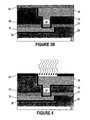
- Figures 3A and 3B show cross sections of an IC employing damascene construction. Figure 3A shows "single damascene" construction whereas Figure 3B shows "dual damascene" construction.
- FIG. 3A depicts a semiconductor substrate 25 having disposed thereon patterned insulator and interconnect layers.
- Inter-layer dielectric (“ILD") 26 contacts semiconductor substrate 25 and provides electrical insulation between semiconductor substrate 25 and first interconnect 30.
- Barrier layer 28 limits diffusion of chemical species between ILD 26 and first interconnect 30.
- Capping layer 32 typically an insulator, covers ILD 26 and first interconnect 30 except where via 34 and barrier layer 36 connect first interconnect 30 to second interconnect 38.
- ILD 35 provides additional electrical isolation between first interconnect 30 and second interconnect 38.
- Capping layer 40 provides both electrical isolation and surface protection to the completed integrated circuit.
- Damascene construction typically begins with semiconductor substrate 25.
- ILD 26 is deposited on semiconductor substrate 25 and planarized using CMP.
- Numerous materials can be employed effectively as ILDs in semiconductor processing. Therefore, without limiting the scope of the present invention, the preferred embodiments of the present invention employ silica-containing materials such as organosilica glasses or doped silica such as fluorine-doped silica glasses.
- barrier layer 28 is deposited in the trench followed by first interconnect 30.
- barrier layers serve to hinder the metal (e.g., copper) from diffusing into adjacent ILDs.
- the material deposited to form barrier layer 28 generally depends on the chemical composition of the interconnect.
- first interconnect 30 comprises tungsten (W)
- barrier layer 28 typically comprises titanium (Ti)-e.g., Ti, titanium nitride (TiN), or a Ti/TiN stack.
- barrier layer 28 typically comprises tantalum (Ta)-e.g., Ta, tantalum nitride (TaN) or a Ta/TaN stack.
- first interconnect 30 comprises copper and barrier layer 28 comprises Ta or TaN or Ta/TaN bilayer, and possibly another layer to increase adhesion between the TaN and the dielectric.
- first interconnect 30 is deposited and then planarized using CMP.
- metal interconnects typically comprise aluminum or copper but may be any material, including metal alloys, that exhibit satisfactory electrical and mechanical properties.
- Capping layer 32 preferably is deposited on first interconnect 30 and ILD 26 following planarization.
- Capping layer 32 typically comprises an insulating capping film, silicon nitride or silicon carbide, and may be patterned using photolithography techniques so as to leave an opening for via 34.
- via 34 may be surrounded by barrier layers.
- Via 34 may comprise the same type of metal used in first interconnect 30 or may be a different material altogether.
- ILD layer 35 (which may or may not be of the same composition as ILD 26) is then deposited on top of capping layer 32, and preferably is further patterned (or etched) to allow for via 34, barrier layer 36, and second interconnect 38.
- the patterning step for ILD 35 and the patterning step for capping layer 32 may be combined in order to speed up fabrication time.
- the composition of barrier layer 36, like barrier 28, is typically selected based upon the materials surrounding it (i.e., via 34), and may therefore comprise the same material as barrier 28 described above.
- Second interconnect 38 fills the remaining trench created in ILD 35.
- Second interconnect 38 may be of the same material as first interconnect 30 and/or via 34, or may be a completely different material altogether.
- first interconnect 30 and second interconnect 38 may be comprised of copper while via 34 may be comprised of tungsten.
- Capping layer 40 is applied above second interconnect 38 following planarization. Although not specifically shown in Figure 3A, capping layer 40 may be patterned, like capping layer 32, in anticipation of subsequent interconnect layers.
- the semiconductor structure shown in Figure 3A is referred to as a "single damascene" or damascene structure because via 34 and second interconnect 38 are formed in separate steps.
- Figure 3B in contrast to Figure 3A, depicts a "dual damascene" structure in which via 34 and second interconnect 38 are formed in a single step and there is no barrier separating them.
- via 34 and second interconnect 38 typically comprise the same material (e.g., copper).
- trench and “recess” are used synonymously herein to indicate a void that may be created in any layer.
- a recess may include additional trenches, for example, in Figure 3A the electrically-insulating layer 35 may have a recess that comprises a secondary trench created for via 34 and a primary trench created for interconnect 38.
- the momentum due to electron flow cause the atoms of the interconnect to migrate in the direction of electron flow along grain boundaries.
- This migration pattern sometimes results in voids (depletions in the conductor at grain boundary intersection point) and hillocks (accumulation of atoms in the conductor at grain boundary intersection points).
- the voids and hillocks produced by electromigration may lead to the failure of an IC by causing open circuits and short circuits of interconnects, respectively.
- Interconnect migration failure may also be the result of stress induced voiding as observed in "Stress Induced Voiding Under Vias Connected to Wide Cu Metal Leads" by E.T. Ogawa et al..
- interfacial surface stress or the stress that exists at the seam of two adjacent layers, is thermally induced and is further exacerbated by electrical stresses. As temperatures and electric stresses fluctuate, the inherent interfacial stress can cause voids at the seam of adjacent layers.
- Voiding resulting from both stress migration and electromigration is especially problematic where the via surface meets the interconnect surface in damascene construction. It is believed that many migration failures occur in the vicinity of the via/interconnect interface. From an electromigration standpoint, as electrons flow from the via to the interconnect or vice versa, the electrons are required to "turn the corner" - i.e., to abruptly change their direction of flow to a narrower path. The reduction of electron path width increases electrical resistance and current crowding, resulting in the heating of the via/interconnect interface and increasing the susceptibility of the interface to migration problems.
- the preferred embodiments of the present invention involve modifications to the interconnects that enhance their mechanical stability.
- the surface of the interconnect is modified rather than the bulk interconnect. Consequently, the interconnect benefits from mechanical stability while retaining the electrical properties of the unmodified interconnect material.
- a number of preferred embodiments are disclosed herein that relate in general to damascene construction and more particularly to specific surfaces on interconnects. Additionally, as will be understood by a person of skill, the techniques and modifications described herein are applicable to any interconnect in an integrated circuit.
- an interconnect layer is implanted with ions in the vicinity of the via/interconnect interface.
- the dual damascene structure of Figure 3B is shown prior to application of the capping layer 40.
- an ion implantation step is performed in the area patterned by mask 42.
- mask 42 restricts ion implantation to the vicinity of the interconnect/via interface.
- a chemical species may be introduced into second interconnect 38 by diffusion or by sputtering.
- second interconnect 38 is copper and the implanted material is selected from the group consisting of arsenic, antimony, chromium, palladium, tin, magnesium, aluminum, cobalt, and zirconium, and combinations thereof.
- implantation depth varies between about 50 and 500 Angstroms and the composition of implanted material in this depth range varies between about 0.1 and about 10 percent by weight.
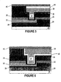
- an alloy layer is deposited on top of second interconnect 38 as shown in Figure 5.
- the dual damascene structure of Figure 3B is shown in which second interconnect 38 has been etched to create a trench and alloy layer 44 has been applied to the trench.
- the etch step may be selective - i.e., confined to a specific area in the vicinity of the interconnect/via interface - or may apply generally to the entire second interconnect 38.
- second interconnect 38 is copper
- alloy layer 44 is a copper alloy comprising copper and a material selected from the group consisting of arsenic, antimony, chromium, palladium, tin, magnesium, aluminum, cobalt, and zirconium, or combinations thereof.
- the thickness of alloy layer 44, or the depth of the trench in second interconnect 38 varies between 50 and 500 Angstroms, and the percent composition of the material added to the copper varies between varies between about 0.1 and about 10 percent by weight.
- a CMP step is performed prior to applying capping layer 40.
- Electroless plating involves metal deposition through a chemical reduction reaction from an aqueous metal salt solution containing also a reducing agent. Deposition temperature is typically between 30 to 80° C. No external power supply is necessary for the metal reduction reaction.
- the semiconductor wafer is immersed in a plating bath, wherein metal ions react with reducing agents on a catalytic surface, thereby enabling plating on interconnects that are electrically isolated.
- Depositing alloy layer 44 in this manner is advantageous because alloy layer 44 is selectively applied to the desired interconnect.
- vapor deposition techniques such as Chemical Vapor Deposition (“CVD”) and Physical Vapor Deposition (“PVD”).
- CVD Chemical Vapor Deposition
- PVD Physical Vapor Deposition
- these techniques involve using a volatile chemical species to create a film at the surface of the semiconductor substrate.
- gross deposition techniques because there is no selectivity of deposition and a film of the material to be deposited forms over the whole surface of the wafer.
- one embodiment that uses vapor deposition techniques to form alloy layer 44 may involve a CMP step after depositing the alloy layer 44 in order to maintain electrical isolation between metal interconnects.
- Another method of maintaining electrical isolation between metal interconnects while using vapor deposition techniques includes employing a mask to limit the deposition of the desired material to only the exposed metal layers. More particularly, the mask may limit the deposition of the desired material to the vicinity of the interconnect/via interface.
- the trench formed prior to the application of alloy layer 44 may be formed by over-polishing during a CMP step, with a desired trench depth of 50 to 500 Angstroms.
- a CMP step may be performed to polish the final surface, and over-polishing used to create the trench in the second interconnect 38 for the alloy layer 44 may be accomplished during this traditional CMP step.
- second interconnect 38 is copper and thin seed layer 46 is a copper alloy comprising copper and a material selected from the group consisting of arsenic, antimony, chromium, palladium, tin, magnesium, aluminum, cobalt, and zirconium and combinations thereof.
- the deposition of alloy layer 46 is accomplished using the selective electroless plating techniques described above.
- alloy layer 46, as shown in Figure 6, or layer 44 in Fig. 5, may be deposited using atomic layer growth methods.
- interfacial stresses at the boundaries between adjacent materials that cause metal migration are more easily activated than other migration inducing phenomena, or have the lower "activation energy.”
- metal layers are about 3000 Angstroms thick, and modifying them to a depth of 500 Angstroms maximum still leaves at least 80% of the metal layer unmodified.
- implantation and deposition methods of the preferred embodiments advantageously modify the interconnect where the interconnect is most susceptible to migration, at the interface between adjacent layers.
- the modified interconnect of the preferred embodiments is not comprised entirely of the alloy material, as was the case in Wang, the overall sheet resistance is decreased.
- An additional benefit of some of the preferred embodiments of the present invention is galvanic corrosion protection.
- galvanic corrosion protection During the course of integrated circuit processing-e.g., during CMP processing-both copper surfaces and barrier metal surfaces may be exposed. Differences in the galvanic potentials of the exposed metals can give rise to a type of corrosion in which the more easily oxidized metal is etched from the wafer surface. This phenomenon is frequently referred to as galvanic corrosion. Because of its galvanic potential, copper is particularly susceptible to galvanic corrosion. Generally speaking, the modification of the top of the interconnect layer according to some of the preferred embodiments, results in copper interconnects with reduced susceptibility to corrosion.
- providing a metal migration inhibiting exterior surface for the interconnect impedes metal movement, thereby eliminating the need for a separate barrier. This could be especially beneficial in next generation ICs, which will likely employ narrower vias so that removing the barrier layer at the bottom and or top surfaces of the via will be particularly desirable.
- interconnect layers processed in manufacturing an IC there are often many interconnect layers processed in manufacturing an IC, and the embodiments disclosed herein may be applied to any or all of those interconnect layers as deemed necessary.
- the IC designers may note a metal migration problem at the first interconnect layer, while the other metal layers do not exhibit such behavior.
- an alloy layer may be employed at the first interconnect according to the embodiments disclosed herein, thereby reducing the potential for excessive limitations of the maximum allowed current density design guidelines for metal interconnect.
Landscapes
- Internal Circuitry In Semiconductor Integrated Circuit Devices (AREA)
- Chemically Coating (AREA)
Abstract
Description
Claims (9)
- A method for constructing an electrical interconnect having enhanced mechanical properties on a semiconductor substrate, comprising:formation of a first recess in an electrically-insulating material;deposition of a first electrically-conductive material in the first recess ;formation of a second recess in the first electrically-conductive material; anddeposition of a second electrically-conductive material in the second recess.
- The method of claim 1, wherein the second electrically-conductive material is deposited by electroless plating.
- The method of claim 2, wherein the depth of the second recess is in the range of about 50 to about 500 Angstroms.
- The method of claim 3, wherein the second electrically-conductive material comprises copper and at least one material selected from the group consisting of arsenic, antimony, chromium, palladium, tin, magnesium, aluminum, cobalt, and zirconium.
- The method of claim 4, wherein copper is present in the second electrically-conductive material at a concentration of between about 95 and about 99.9 weight percent.
- The method of claim 1, wherein the deposition of the second electrically-conductive material is by a vapor deposition technique.
- A method for constructing an electrical interconnect having enhanced mechanical properties on a semiconductor substrate, comprising:formation of a first recess in an electrically-insulating material;deposition of a thin seed layer of a first electrically-conductive material in the first recess;deposition of a second electrically-conductive material in the first recess;formation of a second recess in the second electrically-conductive material; anddeposition of a third electrically-conductive material in the second recess.
- The method of claim 7, wherein the deposition of the thin seed layer occurs by electroless plating.
- A method for constructing an electrical interconnect having enhanced mechanical properties on a semiconductor substrate, comprising:formation of a recess in an electrically-insulating material;deposition of an electrically-conductive material in the recess; andion implantation of a chemical species onto the electrically-conductive material.
Applications Claiming Priority (4)
| Application Number | Priority Date | Filing Date | Title |
|---|---|---|---|
| US39271502P | 2002-06-28 | 2002-06-28 | |
| US392715P | 2002-06-28 | ||
| US288974 | 2002-11-06 | ||
| US10/288,974 US7074709B2 (en) | 2002-06-28 | 2002-11-06 | Localized doping and/or alloying of metallization for increased interconnect performance |
Publications (2)
| Publication Number | Publication Date |
|---|---|
| EP1376685A2 true EP1376685A2 (en) | 2004-01-02 |
| EP1376685A3 EP1376685A3 (en) | 2004-12-22 |
Family
ID=29718516
Family Applications (1)
| Application Number | Title | Priority Date | Filing Date |
|---|---|---|---|
| EP03101890A Withdrawn EP1376685A3 (en) | 2002-06-28 | 2003-06-25 | Localized doping and/or alloying of metallization for increased interconnect performance |
Country Status (3)
| Country | Link |
|---|---|
| US (2) | US7074709B2 (en) |
| EP (1) | EP1376685A3 (en) |
| JP (1) | JP2004040101A (en) |
Cited By (1)
| Publication number | Priority date | Publication date | Assignee | Title |
|---|---|---|---|---|
| DE102007030812B4 (en) * | 2006-09-29 | 2009-08-20 | Hynix Semiconductor Inc., Ichon | Metallic lead in semiconductor device and method of forming same |
Families Citing this family (21)
| Publication number | Priority date | Publication date | Assignee | Title |
|---|---|---|---|---|
| US20040155349A1 (en) * | 2003-01-07 | 2004-08-12 | Naofumi Nakamura | Semiconductor device and method of fabricating the same |
| US7235884B1 (en) * | 2003-04-01 | 2007-06-26 | Altera Corporation | Local control of electrical and mechanical properties of copper interconnects to achieve stable and reliable via |
| US20050006770A1 (en) * | 2003-07-08 | 2005-01-13 | Valeriy Sukharev | Copper-low-K dual damascene interconnect with improved reliability |
| US20050124155A1 (en) * | 2003-12-03 | 2005-06-09 | Brooks Joseph F. | Electrode structures and method to form electrode structures that minimize electrode work function variation |
| US7319071B2 (en) * | 2004-01-29 | 2008-01-15 | Micron Technology, Inc. | Methods for forming a metallic damascene structure |
| JP4178295B2 (en) * | 2004-07-14 | 2008-11-12 | 富士通マイクロエレクトロニクス株式会社 | Semiconductor device having wiring made of copper and method of manufacturing the same |
| WO2006016678A1 (en) | 2004-08-12 | 2006-02-16 | Nec Corporation | Semiconductor device and its manufacturing method |
| JP4377788B2 (en) * | 2004-09-27 | 2009-12-02 | 株式会社神戸製鋼所 | Cu alloy for semiconductor wiring, manufacturing method of Cu alloy wiring, semiconductor device having Cu alloy wiring obtained by the manufacturing method, and sputtering target for forming Cu alloy wiring of semiconductor |
| CN1983550A (en) * | 2005-12-14 | 2007-06-20 | 中芯国际集成电路制造(上海)有限公司 | Method for improving reliability and finished-product rate and eliminating copper offset |
| US7759241B2 (en) * | 2006-09-15 | 2010-07-20 | Intel Corporation | Group II element alloys for protecting metal interconnects |
| JP4506767B2 (en) * | 2007-02-28 | 2010-07-21 | カシオ計算機株式会社 | Manufacturing method of semiconductor device |
| DE102007035834A1 (en) * | 2007-07-31 | 2009-02-05 | Advanced Micro Devices, Inc., Sunnyvale | Semiconductor device with locally increased electromigration resistance in a connection structure |
| DE102008007001B4 (en) * | 2008-01-31 | 2016-09-22 | Globalfoundries Dresden Module One Limited Liability Company & Co. Kg | Increasing the resistance to electromigration in a connection structure of a semiconductor device by forming an alloy |
| JP4656162B2 (en) * | 2008-02-19 | 2011-03-23 | 株式会社デンソー | Waveguide choke structure |
| JP4675393B2 (en) * | 2008-05-12 | 2011-04-20 | パナソニック株式会社 | Semiconductor device and manufacturing method of semiconductor device |
| US8304863B2 (en) * | 2010-02-09 | 2012-11-06 | International Business Machines Corporation | Electromigration immune through-substrate vias |
| US8778408B2 (en) * | 2011-02-18 | 2014-07-15 | Mitsui Chemicals, Inc. | Antimicrobial substance, method for producing same, and antimicrobial material |
| US9711452B2 (en) | 2014-12-05 | 2017-07-18 | International Business Machines Corporation | Optimized wires for resistance or electromigration |
| US9824970B1 (en) * | 2016-06-27 | 2017-11-21 | Globalfoundries Inc. | Methods that use at least a dual damascene process and, optionally, a single damascene process to form interconnects with hybrid metallization and the resulting structures |
| TWI743476B (en) * | 2018-05-04 | 2021-10-21 | 美商應用材料股份有限公司 | Deposition of metal films |
| US12205919B2 (en) | 2021-12-20 | 2025-01-21 | Infineon Technologies Ag | Method of processing a semiconductor wafer, semiconductor die, and method of producing a semiconductor module |
Family Cites Families (18)
| Publication number | Priority date | Publication date | Assignee | Title |
|---|---|---|---|---|
| US4995698A (en) * | 1988-12-30 | 1991-02-26 | Hughes Aircraft Company | Fiber optic canister having orthotropic, controlled thermal expansion bobbin |
| US4955688A (en) * | 1989-03-27 | 1990-09-11 | At&T Bell Laboratories | Optical fiber package and methods of making |
| US5221060A (en) * | 1992-08-14 | 1993-06-22 | Hughes Aircraft Company | Thermal expansion compensated winding of optical fiber canisters |
| US5594829A (en) * | 1995-06-07 | 1997-01-14 | Lostracco; Gregory | Optical fiber dispenser with thermal expansion accommodation layer |
| US6268291B1 (en) * | 1995-12-29 | 2001-07-31 | International Business Machines Corporation | Method for forming electromigration-resistant structures by doping |
| US5822065A (en) * | 1996-07-26 | 1998-10-13 | Litton Systems, Inc. | Conically arranged fiber optic gyroscope coils |
| US5891802A (en) * | 1997-07-23 | 1999-04-06 | Advanced Micro Devices, Inc. | Method for fabricating a metallization stack structure to improve electromigration resistance and keep low resistivity of ULSI interconnects |
| JP3540699B2 (en) | 1998-01-12 | 2004-07-07 | 松下電器産業株式会社 | Method for manufacturing semiconductor device |
| US6367806B1 (en) * | 1999-12-27 | 2002-04-09 | General Electric Company | Seal arrangement for a rotary machine such as a turbine |
| US6420262B1 (en) * | 2000-01-18 | 2002-07-16 | Micron Technology, Inc. | Structures and methods to enhance copper metallization |
| US6525425B1 (en) | 2000-06-14 | 2003-02-25 | Advanced Micro Devices, Inc. | Copper interconnects with improved electromigration resistance and low resistivity |
| US6376353B1 (en) * | 2000-07-03 | 2002-04-23 | Chartered Semiconductor Manufacturing Ltd. | Aluminum and copper bimetallic bond pad scheme for copper damascene interconnects |
| US6387806B1 (en) * | 2000-09-06 | 2002-05-14 | Advanced Micro Devices, Inc. | Filling an interconnect opening with different types of alloys to enhance interconnect reliability |
| FR2816758B3 (en) | 2000-11-14 | 2003-04-04 | Lionel Girardie | COPPER METALLIC PLATING TECHNIQUE FOR TRANSISTOR CONNECTIONS AND INTERCONNECTIONS |
| CN1575508A (en) | 2000-11-15 | 2005-02-02 | 英特尔公司 | Copper alloy interconnections for integrated circuits and methods of making same |
| US6800554B2 (en) * | 2000-12-18 | 2004-10-05 | Intel Corporation | Copper alloys for interconnections having improved electromigration characteristics and methods of making same |
| US6500749B1 (en) * | 2001-03-19 | 2002-12-31 | Taiwan Semiconductor Manufacturing Company | Method to improve copper via electromigration (EM) resistance |
| US6812143B2 (en) * | 2002-04-26 | 2004-11-02 | International Business Machines Corporation | Process of forming copper structures |
-
2002
- 2002-11-06 US US10/288,974 patent/US7074709B2/en not_active Expired - Lifetime
-
2003
- 2003-06-25 EP EP03101890A patent/EP1376685A3/en not_active Withdrawn
- 2003-06-27 JP JP2003183669A patent/JP2004040101A/en active Pending
-
2004
- 2004-06-17 US US10/870,356 patent/US20040224495A1/en not_active Abandoned
Cited By (3)
| Publication number | Priority date | Publication date | Assignee | Title |
|---|---|---|---|---|
| DE102007030812B4 (en) * | 2006-09-29 | 2009-08-20 | Hynix Semiconductor Inc., Ichon | Metallic lead in semiconductor device and method of forming same |
| US7648904B2 (en) | 2006-09-29 | 2010-01-19 | Hynix Semiconductor Inc. | Metal line in semiconductor device and method for forming the same |
| US8120113B2 (en) | 2006-09-29 | 2012-02-21 | Hynix Semiconductor Inc. | Metal line in semiconductor device |
Also Published As
| Publication number | Publication date |
|---|---|
| US20040224495A1 (en) | 2004-11-11 |
| EP1376685A3 (en) | 2004-12-22 |
| US20040002211A1 (en) | 2004-01-01 |
| US7074709B2 (en) | 2006-07-11 |
| JP2004040101A (en) | 2004-02-05 |
Similar Documents
| Publication | Publication Date | Title |
|---|---|---|
| US7074709B2 (en) | Localized doping and/or alloying of metallization for increased interconnect performance | |
| US8766372B2 (en) | Copper-filled trench contact for transistor performance improvement | |
| US6787460B2 (en) | Methods of forming metal layers in integrated circuit devices using selective deposition on edges of recesses and conductive contacts so formed | |
| US8294270B2 (en) | Copper alloy via bottom liner | |
| US7777346B2 (en) | Semiconductor integrated circuit device and a method of manufacturing the same | |
| CN100517684C (en) | Semiconductor device and method for manufacturing same | |
| US7148140B2 (en) | Partial plate anneal plate process for deposition of conductive fill material | |
| US20070132100A1 (en) | Semiconductor device and method for fabricating the same | |
| US8404577B2 (en) | Semiconductor device having a grain orientation layer | |
| JP4886165B2 (en) | Method of selectively alloying interconnect areas by deposition process | |
| US7309651B2 (en) | Method for improving reliability of copper interconnects | |
| US20060001160A1 (en) | Surface treatment of metal interconnect lines | |
| US7235884B1 (en) | Local control of electrical and mechanical properties of copper interconnects to achieve stable and reliable via | |
| US20100289125A1 (en) | Enhanced electromigration performance of copper lines in metallization systems of semiconductor devices by surface alloying | |
| US8836122B2 (en) | Semiconductor device having copper wiring with increased migration resistance | |
| US6756303B1 (en) | Diffusion barrier and method for its production | |
| US6979642B1 (en) | Method of self-annealing conductive lines that separates grain size effects from alloy mobility | |
| US20060228934A1 (en) | Conductive materials for low resistance interconnects and methods of forming the same | |
| US7169706B2 (en) | Method of using an adhesion precursor layer for chemical vapor deposition (CVD) copper deposition | |
| JP2007019555A (en) | Manufacturing method of semiconductor integrated circuit device | |
| KR20030000828A (en) | Method for Forming Line of Semiconductor Device |
Legal Events
| Date | Code | Title | Description |
|---|---|---|---|
| PUAI | Public reference made under article 153(3) epc to a published international application that has entered the european phase |
Free format text: ORIGINAL CODE: 0009012 |
|
| AK | Designated contracting states |
Kind code of ref document: A2 Designated state(s): AT BE BG CH CY CZ DE DK EE ES FI FR GB GR HU IE IT LI LU MC NL PT RO SE SI SK TR |
|
| AX | Request for extension of the european patent |
Extension state: AL LT LV MK |
|
| PUAL | Search report despatched |
Free format text: ORIGINAL CODE: 0009013 |
|
| AK | Designated contracting states |
Kind code of ref document: A3 Designated state(s): AT BE BG CH CY CZ DE DK EE ES FI FR GB GR HU IE IT LI LU MC NL PT RO SE SI SK TR |
|
| AX | Request for extension of the european patent |
Extension state: AL LT LV MK |
|
| AKX | Designation fees paid | ||
| REG | Reference to a national code |
Ref country code: DE Ref legal event code: 8566 |
|
| STAA | Information on the status of an ep patent application or granted ep patent |
Free format text: STATUS: THE APPLICATION IS DEEMED TO BE WITHDRAWN |
|
| 18D | Application deemed to be withdrawn |
Effective date: 20050623 |