EP1376677A2 - Finned heat sinks - Google Patents
Finned heat sinks Download PDFInfo
- Publication number
- EP1376677A2 EP1376677A2 EP03253821A EP03253821A EP1376677A2 EP 1376677 A2 EP1376677 A2 EP 1376677A2 EP 03253821 A EP03253821 A EP 03253821A EP 03253821 A EP03253821 A EP 03253821A EP 1376677 A2 EP1376677 A2 EP 1376677A2
- Authority
- EP
- European Patent Office
- Prior art keywords
- foil
- metallic
- fins
- plate
- preform
- Prior art date
- Legal status (The legal status is an assumption and is not a legal conclusion. Google has not performed a legal analysis and makes no representation as to the accuracy of the status listed.)
- Granted
Links
Images


Classifications
-
- H10W40/226—
-
- B—PERFORMING OPERATIONS; TRANSPORTING
- B23—MACHINE TOOLS; METAL-WORKING NOT OTHERWISE PROVIDED FOR
- B23K—SOLDERING OR UNSOLDERING; WELDING; CLADDING OR PLATING BY SOLDERING OR WELDING; CUTTING BY APPLYING HEAT LOCALLY, e.g. FLAME CUTTING; WORKING BY LASER BEAM
- B23K20/00—Non-electric welding by applying impact or other pressure, with or without the application of heat, e.g. cladding or plating
- B23K20/10—Non-electric welding by applying impact or other pressure, with or without the application of heat, e.g. cladding or plating making use of vibrations, e.g. ultrasonic welding
- B23K20/103—Non-electric welding by applying impact or other pressure, with or without the application of heat, e.g. cladding or plating making use of vibrations, e.g. ultrasonic welding using a roller
-
- F—MECHANICAL ENGINEERING; LIGHTING; HEATING; WEAPONS; BLASTING
- F28—HEAT EXCHANGE IN GENERAL
- F28F—DETAILS OF HEAT-EXCHANGE AND HEAT-TRANSFER APPARATUS, OF GENERAL APPLICATION
- F28F3/00—Plate-like or laminated elements; Assemblies of plate-like or laminated elements
- F28F3/02—Elements or assemblies thereof with means for increasing heat-transfer area, e.g. with fins, with recesses, with corrugations
-
- H10W40/037—
-
- B—PERFORMING OPERATIONS; TRANSPORTING
- B23—MACHINE TOOLS; METAL-WORKING NOT OTHERWISE PROVIDED FOR
- B23K—SOLDERING OR UNSOLDERING; WELDING; CLADDING OR PLATING BY SOLDERING OR WELDING; CUTTING BY APPLYING HEAT LOCALLY, e.g. FLAME CUTTING; WORKING BY LASER BEAM
- B23K2101/00—Articles made by soldering, welding or cutting
- B23K2101/04—Tubular or hollow articles
- B23K2101/14—Heat exchangers
-
- B—PERFORMING OPERATIONS; TRANSPORTING
- B23—MACHINE TOOLS; METAL-WORKING NOT OTHERWISE PROVIDED FOR
- B23K—SOLDERING OR UNSOLDERING; WELDING; CLADDING OR PLATING BY SOLDERING OR WELDING; CUTTING BY APPLYING HEAT LOCALLY, e.g. FLAME CUTTING; WORKING BY LASER BEAM
- B23K2101/00—Articles made by soldering, welding or cutting
- B23K2101/36—Electric or electronic devices
-
- B—PERFORMING OPERATIONS; TRANSPORTING
- B23—MACHINE TOOLS; METAL-WORKING NOT OTHERWISE PROVIDED FOR
- B23P—METAL-WORKING NOT OTHERWISE PROVIDED FOR; COMBINED OPERATIONS; UNIVERSAL MACHINE TOOLS
- B23P2700/00—Indexing scheme relating to the articles being treated, e.g. manufactured, repaired, assembled, connected or other operations covered in the subgroups
- B23P2700/10—Heat sinks
Definitions
- the present invention relates generally to an improved substrate for heat generating electronic and/or semiconductor devices and assemblies, and more particularly to an improved heat dissipating finned substrate for such devices and assemblies.
- the substrate comprises a metallic plate having a plurality of parallelly disposed fins projecting away from the surface and being weldably secured thereto.
- the substrate blank is formed, populated, and otherwise completed prior to final deployment of the fins so as to permit normal production techniques to be practiced, and without requiring special techniques and/or devices to avoid handling interference from the fins.
- an array of spaced parallelly disposed undeployed fin members are created on the heat dissipating surface of a rigid substrate, with the substrate blank thereafter being subjected to various assembly operations including the steps of treating the mounting surface and circuitry and also populating the substrate; all prior to deployment or extension of the fins.
- the substrate blanks of the present invention may be subjected to conventional assembly operations including that of treating the mounting surface and populating the substrate without requiring unusual steps or precautions to be taken to protect the configuration of outwardly extending metallic fins.
- fins In order to enhance the thermal performance of substrate assemblies, metallic fins have typically been added to provide additional surface area for dissipation of thermal energy.
- the utilization of fins provides an additional mechanism for conducting heat away from the substrate member by providing substantially greater surface areas.
- conventional assembly steps and/or operations are impeded or slowed whenever efforts are undertaken to perform work on a finned device, or alternatively to undertake to attach fins to an already-populated support.
- post-attachment of finned members is normally achieved by steps and/or operations which result in the finned members delivering poor thermal performance. For that reason, therefore, finned substrates have met with limited application in the industry.
- an improved outwardly projecting finned heat dissipating substrate is created utilizing preformed fins in a nondeployed configuration, with these fins being weldably secured to the substrate plate or blank prior to deployment.
- the welded attachment provides enhanced thermally conductive properties for the final product.
- the structure of the present invention is arranged such that the fins remain undeployed and coplanar with the substrate until the steps of mounting of the circuit package, semiconductor devices, or other components onto the surface of the substrate is complete. Thereafter, and as a final or near final operation, the fins are deployed so as to be disposed substantially normal to the plane of the substrate.
- the extended or deployed portions of the fins not only remain coplanar with the substrate during the fabrication and assembly operations, but the welded joint provides a highly thermally conductive bond. Since the actual deployment of the fins is undertaken as one of the final steps in the overall operation, assembly proceeds through the production using conventional operations unimpeded by the necessity of protecting or isolating the welded fins during the actual production/assembly steps.
- a thin metallic sheet or foil is superimposed onto the metallic base surface of a substrate blank in order to create a preform assembly.
- the preform is interposed into a work station created between the energy delivery horn of an ultrasonic energy generator and a stable anvil, with the energy delivery horn being in surface-to-surface contact with the sheet or foil.
- An appropriate welding force is applied against the delivery horn while the ultrasonic generator is energized, with the preform being advanced through the work station at a work compatible with formation of continuous, uniform, and integral welded bands.
- the welding steps are repeated, as necessary, in order to create plural parallel spaced apart welded bands.
- the metallic sheet/foil is severed adjacent the same edge surface of each welded band to create unattached metallic sheet/foil spans between mutually adjacent welded bands.
- the semiconductor or circuit package mounting surface is treated, undergoing such operations as creation or refinement of circuitry, device populating steps, and the like.
- the foil spans are folded outwardly until they project normally to the plane of the substrate blank.
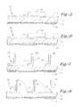
- a subassembly generally designated 10 is illustrated with the subassembly including a rigid metallic aluminum substrate base plate 11 having a dielectric surface 12 bonded to one major surface thereof.
- Circuit foil 13 is bonded or otherwise secured to the surface of dielectric 12 to complete the basic configuration of the support for a heat generated semiconductor device (not shown).
- a thin aluminum metallic sheet 15 is superimposed upon major surface 16 of rigid substrate plate 11, with the thin metallic sheet 15, while in superimposed relationship to surface 16, together with the substrate 11 creating a preform.
- Dielectric 12 is a plastic resinous material which is electrically insulative such as for example epoxy or polyester-based materials which may be filled and/or reinforced, these materials being well known in the art and used as substrate components.
- the preform is placed in working relationship with the energy delivery horn of an ultrasonic generating system, with the horn being illustrated partially in phantom in Figure 2, as at 18.
- Ultrasonic generating systems adapted for ultrasonic welding of metals such as aluminum are, of course, commercially available, with one such system being identified under the trade designation "Ultraseam-20", and offered commercially by American Technology, Inc. of Shelton, CT.
- a stable anvil support 19 which is designed to be sufficiently durable and rigid to provide a work support for the preform of subassembly 10.
- the combination of the ultrasonic energy delivery horn 18 and anvil support 19 create a work station for the welding operation. Support anvils for this purpose are, of course, commercially available and known to those of conventional skill.
- the energy delivery horn 18 is placed into contact with the exposed surface of metallic foil 15 in opposed relationship to work receiving anvil 19 to provide the desired area or surface contact between the delivery horn and the metallic sheet/foil at the predetermined contact point or site.
- a force sufficient to create a working welding pressure at the sheet/plate interface is established and maintained, with this working force and ranges being known to those of skill.
- the ultrasonic vibratory energy dispatched by horn 18 to the site provides the energy and force to create the heat necessary to form the uniform welded zone between the surface of aluminum substrate plate 11 and thin aluminum sheet 15.
- plate 11 will have a thickness dimension ranging from between about 40 and 200 mils, with metallic sheet 15 having a thickness ranging from between about 10 and 20 mils.
- a range of between about 60 and 120 mils for plate 11 and between about 12 and 15 mils for sheet 15 is highly useful.
- continuous relative motion is provided by drawing and/or moving the preform through the work station in order to create the narrow elongated welded band across the entire width of the substrate 11 within the preform and/or assembly 10.
- Welded bands having a width of about one-eighth inch, with bands spaced about one-inch on center have been found to be highly useful for a host of applications. Bands spaced from between one-half inch and one-inch on center have been found useful.
- semiconductor devices may be treated and/or populated onto the insulative surface as at 13 of preform and/or assembly 10.
- operations that may be conducted prior to the folding and/or sheet severing operations are circuit line definition and/or delineation, mounting of semiconductor devices, as well as surface mounting of other components which may be utilized in the overall finished device contemplated.
- fins 28-28 are neither deployed and/or erected until the final stages of the overall operation, thereby rendering the substrate plate more readily usable in conventional production operations.
- the individual steps are undertaken prior to mounting and/or populating the active surface of the assembly.
- the semiconductor devices and other components are not subjected to the conditions which may be employed in fastening, securing, or bonding heat dissipating fins to the surface of a substrate.
Landscapes
- Engineering & Computer Science (AREA)
- Mechanical Engineering (AREA)
- Physics & Mathematics (AREA)
- Thermal Sciences (AREA)
- General Engineering & Computer Science (AREA)
- Cooling Or The Like Of Semiconductors Or Solid State Devices (AREA)
- Lining Or Joining Of Plastics Or The Like (AREA)
- Cooling Or The Like Of Electrical Apparatus (AREA)
- Crystals, And After-Treatments Of Crystals (AREA)
Abstract
Description
Claims (1)
- The method of enhancing the heat dissipating properties of a rigid substrate plate through creation of an array of erect spaced apart parallelly disposed metallic fins projecting from the heat dissipating surface of the rigid substrate plate, with the plate having first and second opposed major surfaces, the first major surface supporting a heat generating semiconductor device, and with said second major surface having said projecting metallic fins weldably attached thereto, said method comprising the steps of:(a) placing a sheet of metallic foil in superimposed relationship to the heat dissipating surface of said substrate plate to create a preform;(b) placing the energy delivery horn of an ultrasonic generating system in closely spaced opposed relationship to the work-receiving surface of a stable anvil to create an ultrasonic welding station;(c) placing said preform within said work station with the semiconductor supporting surface of said preform positioned against said work-receiving surface;(d) bringing said energy delivery horn into contact with the metallic foil surface of said preform in opposed relationship to said work-receiving anvil surface to provide relatively short line contact between said delivery horn and said metallic foil surface at a predetermined contact site;(e) applying a force sufficient for creating a working welding pressure at the foil/plate interface of said preform;(f) coupling an ultrasonic energy generator to said delivery horn for application of vibratory energy at ultrasonic frequencies to said metallic foil at said selected site until said foil/plate interface forms a welded strip bond with laterally spaced apart first and second edges;(g) providing continuous relative motion between said preform and said work station to create a relatively narrow elongated welded band across the width of said substrate;(h) severing said foil along each of said first lateral edge surfaces to form a plurality of mutually adjacent welded foil platelets; and(i) folding each of said foil platelets along said second lateral edge surface to form a family of parallelly disposed spaced-apart heat dissipating metallic foil fins.
Applications Claiming Priority (2)
| Application Number | Priority Date | Filing Date | Title |
|---|---|---|---|
| US172877 | 2002-06-17 | ||
| US10/172,877 US6650215B1 (en) | 2002-06-17 | 2002-06-17 | Finned heat sinks |
Publications (3)
| Publication Number | Publication Date |
|---|---|
| EP1376677A2 true EP1376677A2 (en) | 2004-01-02 |
| EP1376677A3 EP1376677A3 (en) | 2006-03-01 |
| EP1376677B1 EP1376677B1 (en) | 2007-08-01 |
Family
ID=29419908
Family Applications (1)
| Application Number | Title | Priority Date | Filing Date |
|---|---|---|---|
| EP03253821A Expired - Lifetime EP1376677B1 (en) | 2002-06-17 | 2003-06-17 | Finned heat sinks |
Country Status (7)
| Country | Link |
|---|---|
| US (1) | US6650215B1 (en) |
| EP (1) | EP1376677B1 (en) |
| JP (1) | JP4128490B2 (en) |
| AT (1) | ATE368938T1 (en) |
| CA (1) | CA2431520A1 (en) |
| DE (1) | DE60315223T2 (en) |
| TW (1) | TWI250590B (en) |
Families Citing this family (8)
| Publication number | Priority date | Publication date | Assignee | Title |
|---|---|---|---|---|
| US7147041B2 (en) * | 2004-05-03 | 2006-12-12 | Parker-Hannifin Corporation | Lightweight heat sink |
| JP4952070B2 (en) * | 2006-06-02 | 2012-06-13 | ソニー株式会社 | Planar light source device and liquid crystal display device assembly |
| KR101424136B1 (en) * | 2007-09-06 | 2014-08-04 | 삼성전자주식회사 | Heat exchanger for electronic parts having heat-generating fin |
| CN101549435B (en) * | 2008-04-03 | 2012-06-13 | 富准精密工业(深圳)有限公司 | Method for manufacturing heat sink |
| US10919106B2 (en) * | 2017-06-09 | 2021-02-16 | General Electric Company | Ultrasonic welding of annular components |
| JP2019096702A (en) * | 2017-11-21 | 2019-06-20 | トヨタ自動車株式会社 | Cooler |
| US11305373B2 (en) * | 2019-10-30 | 2022-04-19 | Raytheon Company | Ultrasonic additively manufactured coldplates on heat spreaders |
| CN115394657B (en) * | 2022-05-31 | 2024-10-01 | 浙江禾芯集成电路有限公司 | A packaging method for a packaging structure of a planar power device |
Family Cites Families (6)
| Publication number | Priority date | Publication date | Assignee | Title |
|---|---|---|---|---|
| US5533257A (en) * | 1994-05-24 | 1996-07-09 | Motorola, Inc. | Method for forming a heat dissipation apparatus |
| US5791406A (en) * | 1994-08-02 | 1998-08-11 | Hoogovens Aluminium Profiltechnik, Gmbh | Cooling device for electrical or electronic components having a base plate and cooling elements and method for manufacturing the same |
| JPH08130274A (en) * | 1994-10-29 | 1996-05-21 | Shinko Metal Prod Kk | Heat sink |
| US5653280A (en) * | 1995-11-06 | 1997-08-05 | Ncr Corporation | Heat sink assembly and method of affixing the same to electronic devices |
| TW349193B (en) * | 1997-11-14 | 1999-01-01 | Hon Hai Prec Ind Co Ltd | Method of assembling heat sink fins and product thereof |
| JP4355412B2 (en) * | 1999-11-26 | 2009-11-04 | 昭和電工株式会社 | Heat sink and manufacturing method thereof |
-
2002
- 2002-06-17 US US10/172,877 patent/US6650215B1/en not_active Expired - Lifetime
-
2003
- 2003-06-09 CA CA002431520A patent/CA2431520A1/en not_active Abandoned
- 2003-06-13 TW TW092116126A patent/TWI250590B/en not_active IP Right Cessation
- 2003-06-16 JP JP2003170538A patent/JP4128490B2/en not_active Expired - Fee Related
- 2003-06-17 DE DE60315223T patent/DE60315223T2/en not_active Expired - Lifetime
- 2003-06-17 AT AT03253821T patent/ATE368938T1/en not_active IP Right Cessation
- 2003-06-17 EP EP03253821A patent/EP1376677B1/en not_active Expired - Lifetime
Also Published As
| Publication number | Publication date |
|---|---|
| EP1376677A3 (en) | 2006-03-01 |
| ATE368938T1 (en) | 2007-08-15 |
| TWI250590B (en) | 2006-03-01 |
| TW200405483A (en) | 2004-04-01 |
| JP2004023105A (en) | 2004-01-22 |
| EP1376677B1 (en) | 2007-08-01 |
| CA2431520A1 (en) | 2003-12-17 |
| US6650215B1 (en) | 2003-11-18 |
| DE60315223D1 (en) | 2007-09-13 |
| DE60315223T2 (en) | 2007-11-15 |
| JP4128490B2 (en) | 2008-07-30 |
Similar Documents
| Publication | Publication Date | Title |
|---|---|---|
| CN109661723B (en) | Semiconductor package with double-sided heat dissipation structure | |
| US6900077B2 (en) | Methods of forming board-on-chip packages | |
| US20070226996A1 (en) | Hybrid integrated circuit device and method of manufacturing the same | |
| US6650215B1 (en) | Finned heat sinks | |
| WO2016199621A1 (en) | Manufacturing method for power semiconductor device, and power semiconductor device | |
| US7961102B2 (en) | RFID tags for pallets and cartons and system for attaching same | |
| CN100390821C (en) | Method of manufacturing a transponder | |
| US7037753B2 (en) | Non-planar surface for semiconductor chips | |
| US20040014270A1 (en) | Hybrid integrated circuit device | |
| CN100414678C (en) | RFID tag and manufacturing method thereof | |
| CN101334854B (en) | Encapsulation method of electronic label chip | |
| JP3875393B2 (en) | Radiation fin and method of manufacturing the same | |
| US5029747A (en) | Apparatus for replacing defective electronic components | |
| US7468554B2 (en) | Heat sink board and manufacturing method thereof | |
| JPS62217646A (en) | Manufacture of lsi cooling fin | |
| JP2001127201A (en) | Package with radiator and method of forming the same | |
| JP5040269B2 (en) | Laser welding method | |
| JP2004311691A (en) | Metal plate for circuit and ceramic circuit board | |
| JP7587735B2 (en) | Heat sink | |
| WO2025100064A1 (en) | Circuit board and manufacturing method therefor | |
| KR101898479B1 (en) | Method of manufacturing printed circuit board using multi carrier substrates | |
| JP2005123606A (en) | Hybrid integrated circuit device and manufacturing method thereof | |
| JP2000299417A (en) | Heat dissipating metal plate for semiconductor device and method of manufacturing the same | |
| JP2000323637A (en) | Manufacturing method of lead frame with heat sink | |
| TW200419475A (en) | Traffic light with two metal substrates |
Legal Events
| Date | Code | Title | Description |
|---|---|---|---|
| PUAI | Public reference made under article 153(3) epc to a published international application that has entered the european phase |
Free format text: ORIGINAL CODE: 0009012 |
|
| AK | Designated contracting states |
Kind code of ref document: A2 Designated state(s): AT BE BG CH CY CZ DE DK EE ES FI FR GB GR HU IE IT LI LU MC NL PT RO SE SI SK TR |
|
| AX | Request for extension of the european patent |
Extension state: AL LT LV MK |
|
| PUAL | Search report despatched |
Free format text: ORIGINAL CODE: 0009013 |
|
| AK | Designated contracting states |
Kind code of ref document: A3 Designated state(s): AT BE BG CH CY CZ DE DK EE ES FI FR GB GR HU IE IT LI LU MC NL PT RO SE SI SK TR |
|
| AX | Request for extension of the european patent |
Extension state: AL LT LV MK |
|
| 17P | Request for examination filed |
Effective date: 20060901 |
|
| AKX | Designation fees paid |
Designated state(s): AT BE BG CH CY CZ DE DK EE ES FI FR GB GR HU IE IT LI LU MC NL PT RO SE SI SK TR |
|
| GRAP | Despatch of communication of intention to grant a patent |
Free format text: ORIGINAL CODE: EPIDOSNIGR1 |
|
| GRAS | Grant fee paid |
Free format text: ORIGINAL CODE: EPIDOSNIGR3 |
|
| GRAA | (expected) grant |
Free format text: ORIGINAL CODE: 0009210 |
|
| AK | Designated contracting states |
Kind code of ref document: B1 Designated state(s): AT BE BG CH CY CZ DE DK EE ES FI FR GB GR HU IE IT LI LU MC NL PT RO SE SI SK TR |
|
| REG | Reference to a national code |
Ref country code: GB Ref legal event code: FG4D |
|
| REG | Reference to a national code |
Ref country code: CH Ref legal event code: EP |
|
| REG | Reference to a national code |
Ref country code: IE Ref legal event code: FG4D |
|
| REF | Corresponds to: |
Ref document number: 60315223 Country of ref document: DE Date of ref document: 20070913 Kind code of ref document: P |
|
| ET | Fr: translation filed | ||
| PG25 | Lapsed in a contracting state [announced via postgrant information from national office to epo] |
Ref country code: NL Free format text: LAPSE BECAUSE OF FAILURE TO SUBMIT A TRANSLATION OF THE DESCRIPTION OR TO PAY THE FEE WITHIN THE PRESCRIBED TIME-LIMIT Effective date: 20070801 Ref country code: ES Free format text: LAPSE BECAUSE OF FAILURE TO SUBMIT A TRANSLATION OF THE DESCRIPTION OR TO PAY THE FEE WITHIN THE PRESCRIBED TIME-LIMIT Effective date: 20071112 Ref country code: FI Free format text: LAPSE BECAUSE OF FAILURE TO SUBMIT A TRANSLATION OF THE DESCRIPTION OR TO PAY THE FEE WITHIN THE PRESCRIBED TIME-LIMIT Effective date: 20070801 Ref country code: BG Free format text: LAPSE BECAUSE OF FAILURE TO SUBMIT A TRANSLATION OF THE DESCRIPTION OR TO PAY THE FEE WITHIN THE PRESCRIBED TIME-LIMIT Effective date: 20071101 |
|
| NLV1 | Nl: lapsed or annulled due to failure to fulfill the requirements of art. 29p and 29m of the patents act | ||
| REG | Reference to a national code |
Ref country code: CH Ref legal event code: PL |
|
| PG25 | Lapsed in a contracting state [announced via postgrant information from national office to epo] |
Ref country code: CH Free format text: LAPSE BECAUSE OF FAILURE TO SUBMIT A TRANSLATION OF THE DESCRIPTION OR TO PAY THE FEE WITHIN THE PRESCRIBED TIME-LIMIT Effective date: 20070801 Ref country code: AT Free format text: LAPSE BECAUSE OF FAILURE TO SUBMIT A TRANSLATION OF THE DESCRIPTION OR TO PAY THE FEE WITHIN THE PRESCRIBED TIME-LIMIT Effective date: 20070801 Ref country code: LI Free format text: LAPSE BECAUSE OF FAILURE TO SUBMIT A TRANSLATION OF THE DESCRIPTION OR TO PAY THE FEE WITHIN THE PRESCRIBED TIME-LIMIT Effective date: 20070801 |
|
| PG25 | Lapsed in a contracting state [announced via postgrant information from national office to epo] |
Ref country code: BE Free format text: LAPSE BECAUSE OF FAILURE TO SUBMIT A TRANSLATION OF THE DESCRIPTION OR TO PAY THE FEE WITHIN THE PRESCRIBED TIME-LIMIT Effective date: 20070801 |
|
| PG25 | Lapsed in a contracting state [announced via postgrant information from national office to epo] |
Ref country code: GR Free format text: LAPSE BECAUSE OF FAILURE TO SUBMIT A TRANSLATION OF THE DESCRIPTION OR TO PAY THE FEE WITHIN THE PRESCRIBED TIME-LIMIT Effective date: 20071102 Ref country code: DK Free format text: LAPSE BECAUSE OF FAILURE TO SUBMIT A TRANSLATION OF THE DESCRIPTION OR TO PAY THE FEE WITHIN THE PRESCRIBED TIME-LIMIT Effective date: 20070801 |
|
| PG25 | Lapsed in a contracting state [announced via postgrant information from national office to epo] |
Ref country code: PT Free format text: LAPSE BECAUSE OF FAILURE TO SUBMIT A TRANSLATION OF THE DESCRIPTION OR TO PAY THE FEE WITHIN THE PRESCRIBED TIME-LIMIT Effective date: 20080102 Ref country code: SK Free format text: LAPSE BECAUSE OF FAILURE TO SUBMIT A TRANSLATION OF THE DESCRIPTION OR TO PAY THE FEE WITHIN THE PRESCRIBED TIME-LIMIT Effective date: 20070801 Ref country code: CZ Free format text: LAPSE BECAUSE OF FAILURE TO SUBMIT A TRANSLATION OF THE DESCRIPTION OR TO PAY THE FEE WITHIN THE PRESCRIBED TIME-LIMIT Effective date: 20070801 |
|
| PLBE | No opposition filed within time limit |
Free format text: ORIGINAL CODE: 0009261 |
|
| STAA | Information on the status of an ep patent application or granted ep patent |
Free format text: STATUS: NO OPPOSITION FILED WITHIN TIME LIMIT |
|
| PG25 | Lapsed in a contracting state [announced via postgrant information from national office to epo] |
Ref country code: SE Free format text: LAPSE BECAUSE OF FAILURE TO SUBMIT A TRANSLATION OF THE DESCRIPTION OR TO PAY THE FEE WITHIN THE PRESCRIBED TIME-LIMIT Effective date: 20071101 Ref country code: RO Free format text: LAPSE BECAUSE OF FAILURE TO SUBMIT A TRANSLATION OF THE DESCRIPTION OR TO PAY THE FEE WITHIN THE PRESCRIBED TIME-LIMIT Effective date: 20070801 |
|
| 26N | No opposition filed |
Effective date: 20080506 |
|
| PG25 | Lapsed in a contracting state [announced via postgrant information from national office to epo] |
Ref country code: MC Free format text: LAPSE BECAUSE OF NON-PAYMENT OF DUE FEES Effective date: 20080630 |
|
| PG25 | Lapsed in a contracting state [announced via postgrant information from national office to epo] |
Ref country code: IE Free format text: LAPSE BECAUSE OF NON-PAYMENT OF DUE FEES Effective date: 20080617 Ref country code: EE Free format text: LAPSE BECAUSE OF FAILURE TO SUBMIT A TRANSLATION OF THE DESCRIPTION OR TO PAY THE FEE WITHIN THE PRESCRIBED TIME-LIMIT Effective date: 20070801 |
|
| PG25 | Lapsed in a contracting state [announced via postgrant information from national office to epo] |
Ref country code: SI Free format text: LAPSE BECAUSE OF FAILURE TO SUBMIT A TRANSLATION OF THE DESCRIPTION OR TO PAY THE FEE WITHIN THE PRESCRIBED TIME-LIMIT Effective date: 20070801 |
|
| PG25 | Lapsed in a contracting state [announced via postgrant information from national office to epo] |
Ref country code: CY Free format text: LAPSE BECAUSE OF FAILURE TO SUBMIT A TRANSLATION OF THE DESCRIPTION OR TO PAY THE FEE WITHIN THE PRESCRIBED TIME-LIMIT Effective date: 20070801 |
|
| PG25 | Lapsed in a contracting state [announced via postgrant information from national office to epo] |
Ref country code: HU Free format text: LAPSE BECAUSE OF FAILURE TO SUBMIT A TRANSLATION OF THE DESCRIPTION OR TO PAY THE FEE WITHIN THE PRESCRIBED TIME-LIMIT Effective date: 20080202 Ref country code: LU Free format text: LAPSE BECAUSE OF NON-PAYMENT OF DUE FEES Effective date: 20080617 |
|
| PG25 | Lapsed in a contracting state [announced via postgrant information from national office to epo] |
Ref country code: TR Free format text: LAPSE BECAUSE OF FAILURE TO SUBMIT A TRANSLATION OF THE DESCRIPTION OR TO PAY THE FEE WITHIN THE PRESCRIBED TIME-LIMIT Effective date: 20070801 |
|
| PGFP | Annual fee paid to national office [announced via postgrant information from national office to epo] |
Ref country code: DE Payment date: 20120613 Year of fee payment: 10 |
|
| PGFP | Annual fee paid to national office [announced via postgrant information from national office to epo] |
Ref country code: GB Payment date: 20120613 Year of fee payment: 10 Ref country code: FR Payment date: 20120619 Year of fee payment: 10 |
|
| PGFP | Annual fee paid to national office [announced via postgrant information from national office to epo] |
Ref country code: IT Payment date: 20120621 Year of fee payment: 10 |
|
| GBPC | Gb: european patent ceased through non-payment of renewal fee |
Effective date: 20130617 |
|
| REG | Reference to a national code |
Ref country code: FR Ref legal event code: ST Effective date: 20140228 |
|
| REG | Reference to a national code |
Ref country code: DE Ref legal event code: R119 Ref document number: 60315223 Country of ref document: DE Effective date: 20140101 |
|
| PG25 | Lapsed in a contracting state [announced via postgrant information from national office to epo] |
Ref country code: DE Free format text: LAPSE BECAUSE OF NON-PAYMENT OF DUE FEES Effective date: 20140101 Ref country code: GB Free format text: LAPSE BECAUSE OF NON-PAYMENT OF DUE FEES Effective date: 20130617 |
|
| PG25 | Lapsed in a contracting state [announced via postgrant information from national office to epo] |
Ref country code: IT Free format text: LAPSE BECAUSE OF NON-PAYMENT OF DUE FEES Effective date: 20130617 Ref country code: FR Free format text: LAPSE BECAUSE OF NON-PAYMENT OF DUE FEES Effective date: 20130701 |