CROSS REFERENCE TO RELATED APPLICATIONS
This application is a continuation-in-part of, and claims benefit of and
priority from, Application No. 10/100,757, Filed March 19, 2002, titled
"Synchronous Controlled, Self-Timed Local SRAM Block", the complete
subject matter of which is incorporated herein by reference in its entirety.
BACKGROUND OF THE INVENTION
One embodiment of the present invention relates to memory devices.
In particular, one embodiment of the present invention relates to a
synchronously controlled global controller for memory devices.
Memory structures or devices have become integral parts of modern
VLSI systems, including digital line processing systems. Although typically it is
desirable to incorporate as many memory cells as possible into a given area
of a memory structure, memory cell density is usually constrained by other
design factors such as layout efficiency, performance, power requirements,
and noise sensitivity.
In view of the trends toward compact, high-performance, high-bandwidth
integrated computer networks, portable computing, and mobile
communications, the aforementioned constraints may impose severe
limitations upon memory structure designs, which traditional memory
structures and subcomponent implementations may fail to obviate.
A certain amount of time is needed to complete a read or write
operation in such memory structures. After the read or write operation is
complete, additional time is needed to recharge the signals. The minimum
cycle time is achieved if pre-charging starts right after completion of the read
or write operation. However, there is no signal indicating the completion of the
read or write operation. As a result, pre-chargers are generally fired at the
falling edge of a clock pulse, so that the write or read operations must be
completed in the first half of the cycle when the clock pulse is high. In other
words the clock pulse must remain high long enough for the read and write
operations to finish. In the second half of the cycle, when clock is low, the pre-chargers
precharge
Further limitations and disadvantages of conventional and traditional
approaches will become apparent to one of skill in the art, through
comparison of such systems with the present invention as set forth in the
remainder of the present application with reference to the drawings.
SUMMARY OF THE INVENTION
One embodiment of the present invention relates to a global controller
adapted to generate different clock pulses during read and write operations..
In one embodiment, at least one of the clock pulses is extended. In another
embodiment at least one pre-charge signal is skewed for at least a read
operation.
In another embodiment, the present invention relates to a memory
device including at least one local memory block and a global controller (a
synchronously controlled global controller for example) coupled to the local
block. In this embodiment, the global controller is adapted to manage the
timing of a read and write operations (by extending a high portion of a clock
pulse for example).
Still another embodiment relates to a memory structure comprising a
synchronously controlled global element and a self-timed local element. In
this embodiment, the global element comprises at least one synchronously
controlled global controller adapted to extend a portion of at least one clock
pulse. The self-timed local element comprises at least one local memory
block, wherein the local memory block is adapted to communicate with the
global.
Another embodiment of the present invention relates to a method for
processing read and write operations in a memory architecture having at least
a synchronously controlled global controller. The method includes generating
control signals and managing timing during the read and write operations,
including skewing at least one clock pulse so that the read and write
operations are completed in a single cycle.
Yet another embodiment of the present invention includes a method for
processing read and write operations in memory architecture. This method
comprises skewing a clock pulse using a global controller, wherein skewing
the clock pulse includes extending a high portion of the clock pulse using at
least one word line interfacing with the global controller.
Other aspects, advantages and novel features of the present invention,
as well as details of an illustrated embodiment thereof, will be more fully
understood from the following description and drawing, wherein like numerals
refer to like parts.
BRIEF DESCRIPTION OF SEVERAL VIEWS OF THE DRAWINGS
Fig. 1 illustrates a block diagram of an exemplary SRAM module;
Fig. 2 illustrates a block diagram of a SRAM memory core divided into
banks;
Figs. 3A and 3B illustrate SRAM modules including a block structure or
subsystem in accordance with one embodiment of the present invention;
Fig. 4 illustrates a dimensional block array or subsystem used in a
SRAM module in accordance with one embodiment of the present invention;
Fig. 5 illustrates a cell array comprising a plurality of memory cells in
accordance with one embodiment of the present invention;
Fig. 6A illustrates a memory cell used in accordance with one
embodiment of the present invention;
Fig. 6B illustrates back-to-back inventors representing the memory cell
of Fig. 6A in accordance with one embodiment of the present invention;
Fig. 7 illustrates a SRAM module similar to that illustrated Figs. 3A and
3B in accordance with one embodiment of the present invention;
Fig. 8 illustrates a local decoder in accordance with one embodiment of
the present invention;
Fig. 9 illustrates a circuit diagram of a local decoder similar to that
illustrated in Fig. 8 in accordance with one embodiment of the present
invention;
Fig. 10 illustrates a block diagram of the local sense amps and 4:1
muxing in accordance with one embodiment of the present invention;
Fig. 11 illustrates a block diagram of the local sense amps and global
sense amps in accordance with one embodiment of the present invention;
Fig. 12A illustrates a schematic representation of the local sense amps
and global sense amps in accordance with one embodiment of the present
invention;
Fig. 12B illustrates a circuit diagram of an embodiment of a local sense
amp (similar to the local sense amp of Fig. 12A) in accordance with one
embodiment of the present invention;
Fig. 12C illustrates a schematic representation of the amplifier core
similar to the amplifier core illustrated in Fig. 12B;
Fig. 13 illustrates a block diagram of another embodiment of the local
sense amps and global sense amps in accordance with one embodiment of
the present invention;
Fig. 14 illustrates a circuit diagram including a transmission gate of the
4:1 mux similar to that illustrated in Fig. 10 and 12 in accordance with one
embodiment of the present invention;
Fig. 15 illustrates transmission gates of the 2:1 mux coupled to the
inverters of a local sense amp in accordance with one embodiment of the
present invention;
Fig. 16 illustrates the precharge and equalizing portions and
transmission gates of the 2:1 mux coupled to the inverters of a local sense
amp in accordance with one embodiment of the present invention;
Fig. 17 illustrates a circuit diagram of the local sense amp in
accordance with one embodiment of the present invention;
Fig. 18 illustrates a block diagram of a local controller in accordance
with one embodiment of the present invention;
Fig. 19 illustrates a circuit diagram of the local controller in accordance
one embodiment of the present invention;
Fig. 20 illustrates the timing for a READ cycle using a SRAM memory
module in accordance with one embodiment of the present invention;
Fig. 21 illustrates the timing for a WRITE cycle using a SRAM memory
module in accordance with one embodiment of the present invention;
Fig. 22A illustrates a block diagram of local sense amp having 4:1 local
muxing and precharging incorporated therein in accordance with one
embodiment of the present invention;
Fig. 22B illustrates one example of 16:1 muxing (including 4:1 global
muxing and 4:1 local muxing) in accordance with one embodiment of the
present invention;
Fig. 22C illustrates one example of 32:1 muxing (including 8:1 global
muxing and 4:1 local muxing) in accordance with one embodiment of the
present invention;
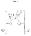
Fig. 23 illustrates a local sense amp used with a cluster circuit in
accordance with one embodiment of the present invention;
Fig. 24 illustrates a block diagram of a memory device having a
synchronously controlled global controller in accordance with one
embodiment of the present invention;
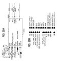
Fig. 25 illustrates a plurality of interconnections for the synchronously
controlled global controller in accordance with one embodiment of the present
invention;
Fig. 26 illustrates a general timing diagram for a write cycle in
accordance with one embodiment of the present invention;
Fig. 27 illustrates a timing diagram for a read cycle in accordance with
one embodiment of the present invention;
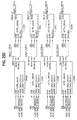
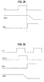
Fig. 28 illustrates a timing diagram for a write cycle having an extended
clock pulse in accordance with one embodiment of the present invention; and
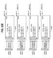
Fig. 29 illustrates a timing diagram for a read cycle having an extended
clock pulse in accordance with one embodiment of the present invention.
DETAILED DESCRIPTION OF THE INVENTION
As will be understood by one skilled in the art, most VLSI systems,
including communications systems and DSP devices, contain VLSI memory
subsystems. Modern applications of VLSI memory subsystems almost
invariably demand high efficiency, high performance implementations that
magnify the design tradeoffs between layout efficiency, speed, power
consumption, scalability, design tolerances, and the like. The present
invention ameliorates these tradeoffs using a novel synchronous, self-timed
hierarchical architecture. The memory module of the present invention also
may employ one or more novel components, which further add to the memory
module's efficiency and robustness.
It should be appreciated that it is useful to describe the various aspects
and embodiments of the invention herein in the context of an SRAM memory
structure, using CMOS SRAM memory cells. However, it should be further
appreciated by those skilled in the art the present invention is not limited to
CMOS-based processes and that these aspects and embodiments may be
used in memory products other than a SRAM memory structure, including
without limitation, DRAM, ROM, PLA, and the like, whether embedded within
a VLSI system, or stand alone memory devices.
EXEMPLARY SRAM MODULE
Fig. 1 illustrates a functional block diagram of one example of a SRAM
memory structure 100 providing the basic features of SRAM subsystems.
Module 100 includes memory core 102, word line controller 104, and memory
address inputs 114. In this exemplary embodiment, memory core 102 is
composed of a two-dimensional array of K-bits of memory cells 103, arranged
to have C columns and R rows of bit storage locations, where K = [C x R]. The
most common configuration of memory core 102 uses single word lines 106 to
connect cells 103 onto paired differential bitlines 118. In general, core 102 is
arranged as an array of 2P entries based on a set of P memory address in.
Thus, the p-bit address is decoded by row address decoder 110 and column
address decoder 122. Access to a given memory cell 103 within such a
single-core memory 102 is accomplished by activating the column 105 by
selecting bitline in the column corresponding to cell 103.
The particular row to be accessed is chosen by selective activation of
row address or wordline decoder 110, which usually corresponds uniquely
with a given row, or word line, spanning all cells 103 in that particular row.
Also, word line driver 108 can drive a selected word line 106 such that
selected memory cell 103 can be written into or read out on a particular pair of
bitlines 118, according to the bit address supplied to memory address inputs
114.
Bitline controller 116 may include precharge cells (not shown), column
multiplexers or decoders 122, sense amplifiers 124, and input/output buffers
(not shown). Because different READ/WRITE schemes are typically used for
memory cells, it is desirable that bitlines be placed in a well-defined state
before being accessed. Precharge cells may be used to set up the state of
bitlines 118, through a PRECHARGE cycle according to a predefined
precharging scheme. In a static precharging scheme, precharge cells may be
left continuously on except when accessing a particular block.
In addition to establishing a defined state on bitlines 118, precharging
cells can also be used to effect equalization of differential voltages on bitlines
118 prior to a READ operation. Sense amplifiers 124 enable the size of
memory cell 103 to be reduced by sensing the differential voltage on bitlines
118, which is indicative of its state, translating that differential voltage into a
logic-lever signal.
In the exemplary embodiment, a READ operation is performed by
enabling row decoder 110, which selects a particular row. The charge on one
of the bitlines 118 from each pair of bitlines on each column will discharge
through the enabled memory cell 103, representing the state of the active
cells 103 on that column 105. Column decoder 122 enables only one of the
columns, connecting bitlines 118 to an output. Sense amplifiers 124 provide
the driving capability to source current to the output including input/output
buffers. When sense amplifier 124 is enabled, the unbalanced bitlines 118 will
cause the balanced sense amplifier to trip toward the state of the bitlines, and
data will be output.
In general, a WRITE operation is performed by applying data to an
input including I/O buffers (not shown). Prior to the WRITE operation, bitlines
118 may be precharged to a predetermined value by precharge cells. The
application of input data to the inputs tend to discharge the precharge voltage
on one of the bitlines 118, leaving one bitline logic HIGH and one bitline logic
LOW. Column decoder 122 selects a particular column 105, connecting
bitlines 118 to the input, thereby discharging one of the bitlines 118. The row
decoder 110 selects a particular row, and the information on bitlines 118 will
be written into cell 103 at the intersection of column 105 and row 106.
At the beginning of a typical internal timing cycle, precharging is
disabled. The precharging is not enabled again until the entire operation is
completed. Column decoder 122 and row decoder 110 are then activated,
followed by the activation of sense amplifier 124. At the conclusion of a READ
or a WRITE operation, sense amplifier 124 is deactivated. This is followed by
disabling decoders 110, 122, at which time precharge cells 120 become
active again during a subsequent PRECHARGE cycle.
POWER REDUCTION AND SPEED IMPROVEMENT
In reference to Fig. 1, the content of memory cell 103 of memory block
100 is detected in sense amplifier 124, using a differential line between the
paired bitlines 118. It should be appreciated that this architecture is not
scalable. Also, increasing the memory block 100 may exceed the practical
limitations of the sense amplifiers 124 to receive an adequate signal in a
timely fashion at the bitlines 118. Increasing the length of bitlines 118
increases the associated bitline capacitance and, thus, increases the time
needed for a voltage to develop thereon. More power must be supplied to
lines 104, 106 to overcome the additional capacitance.
In addition, it takes longer to precharge long bitlines under the
architectures of the existing art, thereby reducing the effective device speed.
Similarly, writing to longer bitlines 118, as found in the existing art, requires
more extensive current. This increases the power demands of the circuit, as
well as reducing the effective device speed.
In general, reduced power consumption in memory devices such as
structure 100 in Fig. 1 can be accomplished by, for example, reducing total
switched capacitance, and minimizing voltage swings. The advantages of the
power reduction aspects of certain embodiments of the present invention can
further be appreciated with the context of switched capacitance reduction and
voltage swing limitation.
SWITCHED CAPACITANCE REDUCTION
As the bit density of memory structures increases, it has been
observed that single-core memory structures may have unacceptably large
switching capacitances associated with each memory access. Access to any
bit location within such a single-core memory necessitates enabling the entire
row, or word line 106, in which the datum is stored, and switching all bitlines
118 in the structure. Therefore, it is desirable to design high-performance
memory structures to reduce the total switched capacitance during any given
access.
Two well-known approaches for reducing total switched capacitance
during a memory structure access include dividing a single-core memory
structure into a banked memory structure, and employing divided word line
structures. In the former approach, it is necessary to activate only the
particular memory bank associated with the memory cell of interest. In the
latter approach, localizing word line activation to the greatest practicable
extent reduces total switched capacitance.
DIVIDED OR BANKED MEMORY CORE
One approach to reducing switching capacitances is to divide the
memory core into separately switchable banks of memory cells. One example
of a memory core 200 divided into banks is illustrated in Fig. 2. In the
illustrated embodiment, the memory core includes two banks of memory cells,
bank #0 and bank #1, generally designated 202 and 204 respectively. The
memory core 200 includes two local decoders 206 that are communicatively
coupled to each other and a global decoder 208 via world line High 210. Each
local decoder 206 includes a local word line High 210 that communicatively
couples the decoder 206 to its associated bank. Additionally, two bank lines
214 are shown communicatively coupled or interfaced to the local decoders
206. It should be appreciated that, in one embodiment, one bank line 214 is
associated with each bank.
Typically, the total switched capacitance during a given memory
access for banked memory cores is inversely proportional to the number of
banks employed. By judiciously selecting the number and placement of the
bank units within a given memory core design, as well as the type of decoding
used, the total switching capacitance, and thus the overall power consumed
by the memory core, can be greatly reduced. Banked design may also realize
a higher product yield. The memory banks can be arranged such that a
defective bank is rendered inoperable and inaccessible, while the remaining
operational banks of the memory core 200 can be packed into a lower-capacity
product.
However, banked designs may not be appropriate for certain
applications. Divided memory cores demand additional decoding circuitry to
permit selective access to individual banks. In other words, such divided
memory cores may demand an additional local decoder 206, local bank line
214 and local word line High 210 for example. Delay may occur as a result.
Also, many banked designs employ memory segments that are merely
scaled-down versions of traditional monolithic core memory designs, with
each segment having dedicated control, precharging, decoding, sensing, and
driving circuitry. These circuits tend to consume much more power in both
standby and operational modes than their associated memory cells. Such
banked structures may be simple to design, but the additional complexity and
power consumption can reduce overall memory component performance.
By their very nature, banked designs are not suitable for scaling-up to
accommodate large design requirements. Also, traditional banked designs
may not be readily adaptable to applications requiring a memory core
configuration that is substantially different from the underlying bank
architecture (e.g., a memory structure needing relatively few rows of long
word lengths). Traditional bank designs are generally not readily adaptable to
a memory structure needing relatively few rows of very long word lengths.
Rather than resort to a top-down division of the basic memory structure
using banked memory designs, one or more embodiments of the present
invention provide a hierarchical memory structure that is synthesized using a
bottom-up approach. Hierarchically coupling basic memory modules with
localized decision-making features that synergistically cooperate to
dramatically reduce the overall power needs, and improve the operating
speed, of the structure. At a minimum, such a basic hierarchical module can
include localized bitline sensing.
DIVIDED WORD LINE
Often, the bit-width of a memory component is sized to accommodate a
particular word length. As the word length for a particular design increases, so
do the associated word line delays, switched capacitance, power
consumption, and the like. To accommodate very long word lines, it may be
desirable to divide core-spanning global word lines into local word lines, each
consisting of smaller groups of adjacent, word-oriented memory cells. Each
local group employs local decoding and driving components to produce the
local word lines when the global word line, to which it is coupled, is activated.
In long word length applications, the additional overhead incurred by divided
word lines can be offset by reduced word line delays.
Rather than resorting to the traditional top-down division of word lines,
certain embodiments of the invention herein include providing a local word
line to the aforementioned basic memory module, which further enhances the
local decision making features of the module. As before, by using a bottom-up
approach to hierarchically couple basic memory modules as previously
described with the added localized decision-making features of local word
lines according to the present invention, additional synergies maybe realized,
which further reduce overall power consumption and signal propagation times.
MULTIPLEXING
One alternative to a banked memory core design is to multiplex or mux
the memory cells. In other words, bits from different words are not stored
sequentially. For example, in 2:1 muxing, bits from two words are stored in an
alternating pattern. For example, if the number 1 represents bits from a first
word, while the number 2 represent bits from a second word. During a READ
or WRITE operation the mux selects which column it is looking at (i.e., the left
or right bit). It should be appreciated that muxing may save space. Banked
designs without muxing require one sense amplifier for every two lines. In 2:1
muxing for example, one sense amplifier is used for every four lines (i.e., one
sense amplifier ties two sets of bitlines together). Muxing enables sense
amps to be shared between muxed cells, which may increase the layout pitch
and area efficiency.
In general, muxing consumes more power than the banked memory
core design. For example, to read a stored word, the mux accesses or
enables an entire row in the cell array, reading all the data stored therein, only
sensing the data needed and disregarding the remainder.
Using a bottom-up approach to hierarchically couple basic memory
modules with muxing according to an embodiment of the present invention,
additional synergies are realized, reducing power consumption and signal
propagation times.
VOLTAGE-SWING REDUCTION TECHNIQUES
Power reduction may also be achieved by reducing the voltage swings
experienced throughout the structure. By limiting voltage swings, it is possible
to reduce the amount of power dissipated as the voltage at a node or on a line
decays during a particular event or operation, as well as to reduce the amount
of power required to return the various decayed voltages to the desired state
after the particular event or operation, or prior to the next access. Two
techniques to this end include using pulsed word lines and sense amplifier
voltage swing reduction.
PULSED WORD LINES
By providing a word line just long enough to correctly detect the
differential voltage across a selected memory cell, it is possible to reduce the
bitline voltage discharge corresponding to a READ operation of the selected
cell. In some designs, by applying a pulsed signal to the associated word line
over a chosen interval, a sense amplifier is activated only during that interval,
thereby reducing the duration of the bitline voltage decay. These designs
typically use some from of pulse generator that produces a fixed-duration
pulse. If the duration of the pulse is targeted to satisfy worst-case timing
scenarios, the additional margin will result in unnecessary bitline current draw
during nominal operations.
Therefore, it may be desirable to employ a self-timed, self-limiting word
line device that is responsive to the actual duration of a given READ operation
on a selected cell, and that substantially limits word line activation during that
duration. Furthermore, where a sense amplifier successfully completes a
READ operation in less than a memory system clock cycle, it may also be
desirable to have asynchronous pulse width activation, relative to the memory
system clock. Certain aspects of the present invention may provide a pulsed
word line signal, for example, using a cooperative interaction between local
decoder and local controller.
SENSE AMPLIFIER VOLTAGE SWING REDUCTION
In order to make large memory arrays, it is most desirable to keep the
size of an individual memory cell to a minimum. As a result, individual memory
cells generally are incapable of supplying a driving current to associated
input/output bitlines. Sense amplifiers typically are used to detect the value of
the data stored in a particular memory cell and to provide the current needed
to drive the I/O lines.
In a sense amplifier design, there typically is a trade-off between power
and speed, with faster response times usually dictating greater power
requirements. Faster sense amplifiers can also tend to be physically larger,
relative to low speed, low power devices. Furthermore, the analog nature of
sense amplifiers can result in their consuming an appreciable fraction of the
total power. Although one way to improve the responsiveness of a sense
amplifier is to use a more sensitive sense amplifier, any gained benefits are
offset by the concomitant circuit complexity which nevertheless suffers from
increased noise sensitivity. It is desirable, then, to limit bitline voltage swings
and to reduce the power consumed by the sense amplifier.
In one typical design, the sense amplifier detects the small differential
signals across a memory cell, which is in an unbalanced state representative
of data value stored in the cell, and amplifies the resulting signal to logic level.
Prior to a READ operation, the bitlines associated with a particular memory
column are precharged to a chosen value. When a specific memory cell is
enabled, a particular row in which the memory cell is located and a sense
amplifier associated with the particular column are selected. The charge on
one of those bitlines associated with the memory cell is discharged through
the enabled memory cell, in a manner corresponding to the value of the data
stored in the memory cell. This produces an imbalance between the signals
on the paired bitlines, causing a bitline voltage swing.
When enabled, the sense amplifier detects the unbalanced signal and,
in response, the usually balanced sense amplifier state changes to a state
representative of the value of the data. This state detection and response
occurs within a finite period, during which a specific amount of power is
dissipated. In one embodiment, latch-type sense amps only dissipate power
during activation, until the sense amp resolves the data. Power is dissipated
as voltage develops on the bitlines. The greater the voltage decay on the
precharged bitlines, the more power dissipated during the READ operation.
It is contemplated that using sense amplifiers that automatically shut off
once a sense operation is completed may reduce power. A self-latching sense
amplifier for example turns off as soon as the sense amplifier indicates the
sensed data state. Latch type sense amps require an activation signal which,
in one embodiment is generated by a dummy column timing circuit. The
sense amp drives a limited swing signal out of the global bitlines to save
power.
REDUNDANCY
Memory designers typically balance power and device area concerns
against speed. High-performance memory components place a severe strain
on the power and area budgets of associated systems, particularly where
such components are embedded within a VLSI system such as a digital signal
processing system. Therefore, it is highly desirable to provide memory
subsystems that are fast, yet power- and area-efficient.
Highly integrated, high performance components require complex
fabrication and manufacturing processes. These processes may experience
unavoidable parameter variations which can impose unwanted physical
defects upon the units being produced, or can exploit design vulnerabilities to
the extent of rendering the affected units unusable or substandard.
In a memory structure, redundancy can be important, because a
fabrication flaw, or operational failure, of even a single bit cell, for example,
may result in the failure of the system relying upon that memory. Likewise,
process invariant features may be needed to insure that the internal
operations of the structure conform to precise timing and parametric
specifications. Lacking redundancy and process invariant features, the actual
manufacturing yield for a particular memory are particularly unacceptable
when embedded within more complex systems, which inheritently have more
fabrication and manufacturing vulnerabilities. A higher manufacturing yield
translates into lower per-unit costs, while a robust design translates into
reliable products having lower operational costs. Thus, it is highly desirable to
design components having redundancy and process invariant features
wherever possible.
Redundancy devices and techniques constitute other certain preferred
aspects of the invention herein that, alone or together, enhance the
functionality of the hierarchical memory structure. The previously discussed
redundancy aspects of the present invention can render the hierarchical
memory structure less susceptible to incapacitation by defects during
fabrication or operation, advantageously providing a memory product that is at
once more manufacturable and cost-efficient, and operationally more robust.
Redundancy within a hierarchical memory module can be realized by
adding one or more redundant rows, columns, or both, to the basic module
structure. Moreover, a memory structure composed of hierarchical memory
modules can employ one or more redundant modules for mapping to failed
memory circuits. A redundant module may provide a one-for-one replacement
of a failed module, or it can provide one or more memory cell circuits to one or
more primary memory modules.
MEMORY MODULE WITH HIERARCHICAL FUNCTIONALITY
The modular, hierarchical memory architecture according to one
embodiment of the present invention provides a compact, robust, power-efficient,
high-performance memory system having, advantageously, a flexible
and extensively scalable architecture. The hierarchical memory structure is
composed of fundamental memory modules or blocks which can be
cooperatively coupled, and arranged in multiple hierarchical tiers, to devise a
composite memory product having arbitrary column depth or row length. This
bottom-up modular approach localizes timing considerations, decision-making,
and power consumption to the particular unit(s) in which the desired
data is stored.
Within a defined design hierarchy, the fundamental memory
subsystems or blocks may be grouped to form a larger memory structure, that
itself can be coupled with similar memory structures to form still larger
memory structures. In turn, these larger structures can be arranged to create
a complex structure, including a SRAM module, at the highest tier of the
hierarchy. In hierarchical sensing, it is desired to provide two or more tiers of
bit sensing, thereby decreasing the READ and WRITE time of the device, i.e.,
increasing effective device speed, while reducing overall device power
requirements. In a hierarchical design, switching and memory cell power
consumption during a READ/WRITE operation are localized to the immediate
vicinity of the memory cells being evaluated or written, i.e., those memory
cells in selected memory subsystems or blocks, with the exception of a limited
number of global word line selectors, sense amplifiers, and support circuitry.
The majority of subsystems or blocks that do not contain the memory cells
being evaluated or written generally remain inactive.
Alternate embodiments of the present invention provide a hierarchical
memory module using local bitline sensing, local word line decoding, or both,
which intrinsically reduces overall power consumption and signal propagation,
and increases overall speed, as well as increasing design flexibility and
scalability. Aspects of the present invention contemplate apparatus and
methods which further limit the overall power dissipation of the hierarchical
memory structure, while minimizing the impact of a multi-tier hierarchy.
Certain aspects of the present invention are directed to mitigate functional
vulnerabilities that may develop from variations in operational parameters, or
that related to the fabrication process.
HIERARCHICAL MEMORY MODULES
In prior art memory designs, such as the aforementioned banked
designs, large logical memory blocks are divided into smaller, physical
modules, each having the attendant overhead of an entire block of memory
including predecoders, sense amplifiers, multiplexers, and the like. In the
aggregate, such memory blocks would behave as an individual memory block.
However, using the present invention, SRAM memory modules of
comparable, or much larger, size can be provided by coupling hierarchical
functional subsystems or blocks into larger physical memory modules of
arbitrary number of words and word length. For example, existing designs that
aggregate smaller memory modules into a single logical modules usually
require the replication of the predecoders, sense amplifiers, and other
overhead circuitry that would be associated with a single memory module.
According to the present invention, this replication is unnecessary, and
undesirable. One embodiment of the present invention comprehends local
bitline sensing, in which a limited number of memory cells are coupled with a
single local sense amplifier, thereby forming a basic memory module. Similar
memory modules are grouped and arranged to form blocks that, along with
the appropriate circuitry, output the local sense amplifier signal to the global
sense amplifier. Thus, the bitlines associated with the memory cells in the
block are not directly coupled with a global sense amplifier, mitigating the
signal propagation delay and power consumption typically associated with
global bitline sensing. In this approach, the local bitline sense amplifier quickly
and economically sense the state of a selected memory cell in a block and
reports the state to the global sense amplifier.
In another embodiment of the invention herein, providing a memory
block, a limited number of memory cells, among other units. Using local word
line decoding mitigates the delays and power consumption of global word line
decoding. Similar to the local bitline sensing approach, a single global word
line decoder can be coupled with the respective local word line decoders of
multiple blocks. When the global decoder is activated with an address, only
the local word line decoder associated with the desired memory cell of a
desired block responds, activating the memory cell. This aspect, too, is
particularly power-conservative and fast, because the loading on the global
line is limited to the associated local word line decoders, and the global word
line signal need be present only as long as required to trigger the relevant
local word line. In yet another embodiment of the present invention, a
hierarchical memory block employing both local bitline sensing and local word
line decoding is provided, which realizes the advantages of both approaches.
Each of the above embodiments among others, is discussed below.
SYNCRHONOUS CONTROLLED SELF-TIMED SRAM
One embodiment of a 0.13µm SRAM module, generally designated
300, is illustrated in Figs. 3A and 3B. It should be appreciated that, while a
0.13µm SRAM module is illustrated, other sized SRAM modules are
contemplated. The illustrated SRAM embodiment comprises a hierarchical
memory that breaks up a large memory into a two-dimensional array of
blocks. In this embodiment, a row of blocks is designated a row block while a
column of blocks is designated a column block. A pair of adjacent row blocks
302 and column blocks 304 is illustrated.
It should be appreciated that the terms row blocks and block columns
are arbitrary designations that are assigned to distinguish the blocks
extending in one direction from the blocks extending perpendicular thereto,
and that these terms are independent of the orientation of the SRAM 300. It
should also be appreciated that, while four blocks are depicted, any number of
column and row blocks are contemplated. The number of blocks in a row
block may generally range anywhere from 1 to 16, while the number of blocks
in a column block may generally range anywhere from 1 to 16, although larger
row and column blocks are contemplated.
In one embodiment, a block 306 comprises at least four entities: (1)
one or more cell arrays 308; (2) one or more local decoders 310 (alternatively
referred to as "LxDEC 710"); (3) one or more local sense amps 312
(alternatively referred to as "LSA 712"); and (4) one or more local controllers
314 (alternatively referred to as "LxCTRL 714"). In an alternative
embodiment, the block 306 may include clusters as described below.
SRAM 300 illustrated in Figs. 3A and 3B includes two local
predecoders 316 (alternatively referred to as "LxPRED"), three global
decoders 318 (alternatively referred to as "GxDEC"), a global predecoder 320
(alternatively referred to as "GxPRED"), two global controllers 322
(alternatively referred to as "GxCTR"), and two global sense amps 324
(alternatively referred to as "GSA 724") in addition to the illustrated block 306
comprising eight cell arrays 308, six local decoders 310, eight local sense
amps 312, and two local controllers 314. It should be appreciated that one
embodiment comprise one local sense amp (and in one embodiment one 4:1
mux) for every four columns of memory cell, each illustrated global controller
comprises a plurality of global controllers, one global controller for each local
controller, and each illustrated local controller comprises a plurality of local
controllers, one for each row of memory cells.
An alternative embodiment of block 306 comprising only four cell
arrays 308, two local decoders 310, two local sense amps 312, and one local
controller 314 is illustrated in Fig. 4. Typically, the blocks range in size from
about 2 Kbits to about 150 Kbits.
In one embodiment, the blocks 306 may be broken down further into
smaller entities. One embodiment includes an array of sense amps arranged
in the middle of the cell arrays 308, dividing the cell arrays into top and bottom
sub-blocks as discussed below.
It is contemplated that, in one embodiment, the external signals that
control each block 300 are all synchronous. That is, the pulse duration of the
control signals are equal to the clock high period of the SRAM module.
Further, the internal timing of each block 300 is self-timed. In other words the
pulse duration of the signals are dependent on a bit-line decay time and are
independent of the clock period. This scheme is globally robust to RC effects,
locally fast and power-efficient as provided below
MEMORY CELL
In one embodiment the cell arrays 308 of the SRAM 300 comprises a
plurality of memory cells as illustrated in Fig. 5, where the size of the array
(measured in cell units) is determined by rows x cols. For example, a megabit
memory cell array comprises a 1024x1024 memory cells. One embodiment of
a memory cell used in the SRAM cell array comprises a six-transistor CMOS
cell 600A (alternatively referred to as "6T cell") is illustrated in Fig. 6A. In the
illustrated embodiment, 6T cell 600 includes transistors 601a, 601b, 601c and
601d.
Each 6T cell 600 interfaces to a local wordline 626 (alternatively
referred to as lwlH), shared with all other 6T cells in the same row in a cell
array. A pair of local bitlines, designated bit and bit_n and numbered 628 and
630 respectively, are shared with all other 6T cells 600 in the same column in
the cell array. In one embodiment, the local wordline signal enters each 6T
cell 600 directly on a poly line that forms the gate of cell access transistors
632 and 634 as illustrated. A jumper metal line also carries the same local
wordline signal. The jumper metal line is shorted to the poly in strap cells that
are inserted periodically between every 16 or 32 columns of 6T cells 600.
The poly in the strap cells is highly resistive and, in one embodiment of the
present invention, is shunted by a metal jumper to reduce resistance.
In general, the 6T cell 600 exists in one of three possible states: (1) the
STABLE state in which the 6T cell 600 holds a signal value corresponding to
a logic "1" or logic "0"; (2) a READ operation state; or (3) a WRITE operation
state. In the STABLE state, 6T cell 600 is effectively disconnected from the
memory core (e.g., core 102 in Fig. 1). In one example, the bit lines, i.e., bit
and bit_n lines 628, 630 respectively, are precharged HIGH (logic "1") before
any READ or WRITE operation takes place. Row select transistors 632, 634
are turned off during precharge. Local sense amplifier block (not shown but
similar to LSA 712) is interfaced to bit line 628 and bit_n line 630, similar to
LSA 712 in Figs. 3A, 3B and 4, supply precharge power.
A READ operation is initiated by performing a PRECHARGE cycle,
precharging bit line 628 and bit_n line 630 to logic HIGH, and activating LwLH
626 using row select transistors 632, 634. One of the bitlines discharges
through 6T cell 600, and a differential voltage is setup between bit line 628
and bit_n line 630. This voltage is sensed and amplified to logic levels.
A WRITE operation to 6T cell 600 is carried out after another
PRECHARGE cycle, by driving bitlines 628, 630 to the required state,
corresponding to write data and activating IwlH 626. CMOS is a desirable
technology because the supply current drawn by such an SRAM cell typically
is limited to the leakage current of transistors 601a-d while in the STABLE
state.
Fig. 6B illustrates an alternative representation of the 6T cell illustrated
in Fig. 6A. In this embodiment, transistors 601a, 601b, 601c and 601d are
represented as back-to- back inventors 636 and 638 respectively as illustrated.
LOCAL DECODER
A block diagram of one embodiment of a SRAM module 700, similar to
the SRAM module 300 of Figs. 3A, 3B and 4, is illustrated in Fig. 7. This
embodiment includes a one-dimensional array of local x-decoders or LxDEC
710 similar to the LxDEC 310. The LxDEC 710 array is physically arranged as
a vertical array of local x-decoders located proximate the cell array 708. The
LxDEC 710 interfaces with or is communicatively coupled to a global decoder
or GxDEC 718.
In one embodiment, the LxDEC 710 is located to the left of the cell
array 708. It should be appreciated that the terms "left," or "right," "up," or
"down," "above," or "below" are arbitrary designations that are assigned to
distinguish the units extending in one direction from the units extending in
another direction and that these terms are independent of the orientation of
the SRAM 700. In this embodiment, LxDEC 710 is in a one-to-one
correspondence with a row of the cell array 708. The LxDEC 710 activates a
corresponding local wordline or lwlH 726 not shown of a block. The LXDEC
710 is controlled by, for example, WIH, bnkL and BitR 742 signals on their
respective lines.
Another embodiment of LxDEC 710 is illustrated in Fig. 8. In this
embodiment, each LxDEC 710 in a block interfaces to a unique global
wordline 750 (alternatively referred to as "WIH") corresponding to the memory
row. The global WIH 750 is shared with other corresponding LxDEC's 710 in
the same row block using lwlH 750. LxDEC 710 only activates the local
wordline 726, if the corresponding global wordline 750 is activated. It should
be appreciated that a plurality of cells 754 similar to the 6T cells discussed
previously, are communicatively coupled to the lwlH 726 as illustrated.
In the embodiment illustrated in Fig. 8., every LxDEC 710 in the top or
bottom of a sub-block shares the same bank line (alternatively referred to as
"bnk Sol H"). It should be appreciated that there are separate bnkL_bot 756
and bnkL_top 758 lines for the bottom and top sub-blocks, respectively.
LxDEC 710 will only activate lwlH 726 if this line is active. The bank lines are
used to selectively activate different blocks within the same row block and
synchronize the proper access timing. For example, during a READ operation,
the bank line will activate as early as possible to begin the read operation.
During a WRITE operation for example, bnkL is synchronized to the
availability of the data on the local bitlines.
Every LxDEC 710 in the embodiment illustrated in Fig. 8 shares the
same bitR line 760. This line is precharged to VDD in the memory idle state.
When bitR 760 approaches VDD/2 (i.e., one half of VDD), it signals the end of
a memory access and causes the LXDEC 710 to de-activate lwlH 726. The
bitR signal line 760 is constructed as a replica to the bitlines (i.e, in this
embodiment bit line 728 and bit_n line 730 are similar to bit line 628 and bit_n
line 630 discussed previously) in the cell array, so the capacitive loading of
the bitR 760 line is the same per unit length as in the cell array. In one
embodiment, a replica local decoder, controlled by bnkL, fires the lwlRH. In
this embodiment, the lwlRH is a synchronization signal that controls the local
controller. The lwlRH may fire every time an associated subblock
(corresponding to a wlRH) is accessed.
In one embodiment, a global controller initiates or transmits a READ or
WRITE signal. The associated local controller 714 initiates or transmits an
appropriate signal based on the signal transmitted by the global controller (not
shown). The local controller pulls down bitR line 760 from LxDEC 710 when
the proper cell is READ from or WRITTEN to, saving power. When the
difference between bit line 728 and bit_n line 730 is high enough to trigger the
sense amp portion, the lwlH 726 is turned off to save power. A circuit diagram
of one embodiment of a local x-decoder similar to LxDEC 710 is illustrated in
Fig. 9.
LOCAL SENSE-AMPS
One embodiment of the SRAM module includes a one-dimensional
array of local sense-amps or LSA's 712 illustrated in Figs. 10 and 11, where
the outputs of the LSA 712 are coupled to the GSA 724 via line 762. In one
embodiment, the outputs of the LSA's are coupled to the GSA via at least a
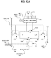
pair of gbit and gbit_n lines. Fig. 12A illustrates one embodiment of LSA 712
comprising a central differential cross-coupled amplifier core 764, comprising
two inverters 764A and 764B. The senseH lines 766, and clusterL 798, are
coupled to the amplifier core through transistor 771.
The LSA's 764 are coupled to one or more 4:1 mux's 772 and eight
pairs of muxL lines 768A, four muxLs 768A located above and four 768B
(best viewed in Fig. 7) located below the amplifier core 764. In the illustrated
embodiment, each of the bitline multiplexers 772 connects a corresponding
bitline pair and the amplifier core 764. T he gbit and gbit_n are connected to
the amplifier core through a PMOS transistors (transistors 770 for example).
When a bitline pair is disconnected from the amplifier core 764, the bitline
multiplexer 772 actively equalizes and precharges the bitline pair to VDD.
Fig. 12B illustrates a circuit diagram of an amplifier core 764 having
two inverters 764A and 764B, where each inverter 764A and 764B is coupled
to a SenseH line 766 and cluster line 798 through a transistor NMOS 771.
Only one sense H cluster lines are illustrated. In the illustrated embodiment,
each of the inverters 764A and 764B are represented as coupled PMOS and
NMOS transistor as is well known in the art. Fig. 12C illustrates a schematic
representation of the amplifier core of Fig. 12B (similar to the amplifier core of
Fig. 12A).
In one embodiment illustrated in Fig. 13, the sense-amp array
comprises a horizontal array of sense-amps 713 located in the middle of the
cell array 708, splitting the cell array into top 708A and bottom 708B sub-blocks
as provided previously. In this embodiment, the width of a single LSA
712 is four times the width of the cell array, while the number of LSA 712
instances in the array is equal to the number of cols/4. That is, each LSA 712
(and in one embodiment one 4:1 mux) is in a one-to-one correspondence with
four columns of the cell array and interfaces with the corresponding local
bitline-pairs of the cell array 708 in the top and bottom sub-blocks 708A,
708B. This arrangement is designated 4:1 local multiplexing (alternatively
referred to as "4:1 local muxing"). It should be appreciated that the bitline-pairs
of the bottom sub-block 708B are split from the top sub-block 708A,
thereby reducing the capacitive load of each bitline 729 by a factor of two,
increasing the speed of the bitline by the same factor and decreasing power.
One embodiment of the 4:1 mux plus precharge is illustrated in Figs. 10 and
12 and discussed in greater detail below.
It is currently known to intersperse power rails 774 (shown in phantom)
between pairs of bitlines to shield the bitline pairs from nearby pairs. This
prevents signals on one pair of bitlines from affecting the neighboring bitline
pairs. In this embodiment, when a pair of bitlines 729 (bit and bit_n, 728, 730)
is accessed, all the neighboring bitlines are precharged to VDD by the 4:1
mux as illustrated in Fig. 12. Precharging the neighboring bitlines, eliminates
the need for shields to isolate those bitlines. This means that it is not
necessary to isolate pairs of bitlines from each other using with interspersed
power rails 774. This allows for a larger bitline pitch in the same total width,
and therefore less capacitance, less power, and higher speed.
The LSA 712 interfaces with a pair of global bitlines, designated gbit
776 and gbit_n 778 via a PMOS transistors 770 as illustrated in Fig. 12A. Two
PMOS transistors are illustrated, but any number is contemplated. In one
embodiment, the global bitlines run vertically in parallel with the local bitlines.
The global bitlines are shared with the corresponding local sense-amps 712 in
other blocks in the same column block. In one embodiment, the local bitlines
and global bitlines are routed on different metal layers. Because there are four
times fewer global bitlines than local bitlines, the global bitlines are physically
wider and placed on a larger pitch. This significantly reduces the resistance
and capacitance of the long global bitlines, increasing the speed and reliability
of the SRAM module. The PMOS transistors 770 isolate global bitlines 776,
778 from the sense amp.
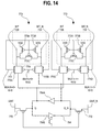
One embodiment of the bitline multiplexer or 4:1 mux 772 is illustrated
in Fig. 14. In this embodiment, the 4:1 mux 772 comprises a precharge and
equalizing portion or device 773 and two transmission gates per bit/bit_n pair.
More specifically, 4:1 muxing may comprise 8 transmission gates and 4
precharge and equalizers, although only 4 transmission gates and 2
precharge and equalizers are illustrated.
In the illustrated embodiment, each precharge and equalizing portion
773 of the 4:1 mux comprises three PFet transistors 773A, 773B and 773C. In
this embodiment, the precharge portion comprises PFet transistors 773A and
773B. The equalizing portion comprises PFet transistor 773D.
In the illustrated embodiment, each transmission gate comprises one
NFet 777A and one PFet 777B transistor. While a specific number and
arrangement of PMOS and NMOS transistors are discussed, different
numbers and arrangements are contemplated. The precharge and equalizing
portion 773 is adapted to precharge and equalize the bitlines 728, 739 as
provided previously. The transmission gate 775 is adapted to pass both logic
"1"'s and "0"'s as is well understood in the art. The NFet transistors, 777A and
777B for example, may pass signals during a WRITE operation, while the
PFet transistors 779A and 779B may pass signals during a READ operation.
Fig. 15 and 16 illustrate embodiments of the 2:1 mux 772 coupled to
the amplifier core 764 of the LSA. Fig. 15 also illustrates an alternate
representation of the transmission gate. Here, four transmission gates 775A,
775B, 775C and 775D are illustrated coupled to the inverters 764A and 764B
of the inverter core. In one embodiment of the present invention, eight
transmission gates are contemplated for each LSA, two for each bitline pair.
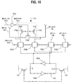
Fig. 16 illustrates the precharge and equalizing portion 773 of the 2:1
coupled to the transmission gates 775A and 775B of mux 772, which in turn is
coupled to the amplifier core. While only one precharge and equalizing portion
773 is illustrated, it is contemplated that a second precharge and equalizing
portion 773 is coupled to the transmission gates 775C and 775D.
In one embodiment illustrated in Fig. 7, the LSA 712 is controlled by
the following set of lines, or signals on those lines, that are shared across the
entire LSA 712 array: (1) muxL_bot 768B; (2) muxL_top 768A; (3) senseH
766; (4) genL 780; and (5) lwlRH 782. In one embodiment of the SRAM
module, the LSA 712 selects which of the local bitlines to use to initiate or
access the cell array 708. The local bitlines comprise 8 pairs of lines, 4 pairs
of mux lines 768B that interface to the bottom sub-block 708B (alternatively
referred to as "muxL_bot 765B<0:3>") and 4 pairs of mux lines 768A that
interface to the top sub-block 708A (alternatively referred to as "muxL_top
765A<0:3>"). The LSA 712 selects which of the 8 pairs of local bitlines to use
for the current access. The LSA 712 maintains any local bitline not selected
for access in a precharged and equalized state. In one embodiment, the LSA
712 keeps the non-selected bitlines precharged to VDD.
The LSA 712 also activates the amplifier portion of the sense-amp 713
using a sense enable line 766 or signal on the line (alternatively referred to as
"senseH 766") connected to transistor 773. This activation signal is distributed
into four separate signals, each signal tapping one out of every four local
sense-amps. In one embodiment, the local controller 714 may activate all the
senseH lines 766 simultaneously (designated "1:1 global multiplexing" or "1:1
global mux") because every sense-amp 713 is activated by senseH lines 766
for each access. Alternately, the local controller may activate the senseH lines
766 in pairs (designated "2:1 global multiplexing" or "2:1 global mux") because
every other sense-amp 713 is activated by senseH 766 for each access.
Additionaly, the LSA 712 may activate the senseH 766 lines 766 individually
(designated "4:1 global multiplexing" or "4:1 global mux"), because every
fourth sense-amp is activated for each access. It should be appreciated that
connecting or interfacing the senseH 766 to every fourth enabled transistor in
4:1 global multiplexing provides for more configurable arrangements for
different memory sizes.
The LSA 712, in one embodiment, exposes the sense-amps 713 to the
global bitlines. The LSA 712 activates or initiates the genL line 780, thus
exposing the sense amps 713 to the gbit and gbit_n.
In one embodiment, the LSA 712 replicates the poly local wordline
running through each row of each block. This replicated line is referred to as a
dummy poly line 782 (alternatively referred to as "lwlRH 782"). In this
embodiment, the lwlRH line 782 forms the gate of dummy transistors that
terminate each column of the cell array 708. Each dummy transistor replicates
the access transistor of the 6T SRAM cell. The capacitive load of this line is
used to replicate the timing characteristics of an actual local wordline.
It is contemplated that, in one embodiment, the replica lwlRH line 782
also extends to the metal jumper line (not shown). The replica jumper line has
the same width and neighbor metal spacing as any local wordline jumper in
the cell array. This line is used strictly as a capacitive load by the local
controller 714 and does not impact the function of the LSA 712 in any way.
More specifically, the replica jump line is adapted to reduce the resistance of
the lwlRH poly line similar to the metal shunt line as provided earlier. A circuit
diagram of one embodiment of an LSA 712 is illustrated in Fig. 17.
LOCAL CONTROLLER
In one embodiment, each block has a single local controller or LxCTRL
714 as illustrated in Figs. 7 and 18 that coordinates the activities of the local
x-decoders 710 and sense-amps 713. In this embodiment, the LxCTRL 714
coordinates such activities by exercising certain lines including: (1) the bitR
760; (2) the bnkL_bot 756; (3) the bnkL_top 758; (4) the muxL_bot 765B; (5)
the muxL_top 765A; (6) the senseH 766; (7) the genL 780; and (8) the lwlRH
782 control lines as illustrated in Fig. 7. Each of these lines is activated by a
driver and control logic circuit in the LxCTRL circuit 714. In one embodiment,
all these lines are normally inactivate when the SRAM module is in the idle
state except for the genL line 780. The genL line 780 is active in the idle state.
The LxCTRL 714 circuit is in turn activated by external Vertical and Horizontal
signals. Vertical signals include: (1) lmuxL 784; (2) gmuxL 786; (3) rbankL
788; (4) gbitR 760; and (5) wbankL 792 signals. Horizontal signals include: (1)
wlRH 794; (2) blkSelH_bot 756; and (3) blkSelH_top 758.
In one embodiment, all LxCTRL 714 circuits in the same column block
share the Vertical signals. In this embodiment, the LxCTRL 714 in each block
interfaces with four local mux lines 784 (alternatively referred to as
"lmuxL<0:3>" or "Imuxl"). Only one of the four ImuxL lines 768 is active at any
time. The LxCTRL 714 initiates or activates one lmuxL lines 768 to access a
cell array 708, selecting one of the four cell array columns interfaced to each
LSA 712 for access.
In one embodiment, similar to that discussed previously, the LSA 712
may activate the senseH 766 signals individually (i.e., 4:1 global multiplexing).
In this embodiment, the LxCTRL 714 in each block interfaces with four global
mux lines 786 (alternatively referred to as "gmuxL<0:3>" or "gmuxl"). It should
be appreciated that only one of these four gmuxL lines 768 is active at any
time, selecting or activating one out of every four global bitlines for access. In
one embodiment the LSA 712 activates the senseH lines 766 in pairs (i.e., 2:1
global multiplexing). In this embodiment only two of the four gmuxL lines 768
are active at any time, selecting one out of every two global bitlines for
access. For 1:1 global muxing, all four gmuxL lines 786 are always active,
selecting all the global bitlines for access.
All LxCTRL circuits 714 in the same column block share the same read
bank lines 788 or signals on the lines (alternatively designated "rbankL"). The
rbankL line 788 is activated when a READ operation is requested (i.e., data is
read from the block). At the end of the READ operation, the global bitlines
selected by the gmuxL line 768s 786 contain limited swing differential signals.
This limited swing differential signals represent the stored values in the cells
selected by the lwlH line 726 and the lmuxL lines 784.
In one embodiment, a global bit replica line 790 or signal on the line is
shared with all the LxCTRL circuits 714 in the same column block
(alternatively designated "gbitR"). The gbitR line 760 is maintained externally
at VDD when the SRAM memory is idle. The gbitR line 760 is made floating
when a READ access is initiated. The LxCTRL 714 discharges this signal to
VSS when a READ access request is concluded synchronous with the
availability of READ data on gbit/gbit_n.
During a WRITE operation, the LxCTRL 714 activates write bank lines
792 or signals on the line (alternatively referred to as "wbnkL"). Limited swing
differential signals are present on the global bitlines when the wbnkL line 792
is activated. The limited swing differential signals represent the data to be
written.
It should be further appreciated that, in one embodiment, all the
LxCTRL circuits 714 in the same row block column share the Horizontal
signals. In one embodiment, all the LxCTRL 714 circuits share a replica of the
global wordline wlH line 794 (alternatively referred to as "wlRH") that runs
through each row of the memory. The physical layout of the wlRH line 794
replicates the global wordline in each row with respect to metal layer, width,
and spacing. Thus the capacitive loading of the wlRH 794 and the global wlH
signal are the same. On every memory access, the wlRH line 794 is activated
simultaneously with a single global wlH for one row in the block.
The LxCTRL 714 indicates to the block whether the bottom or top sub-block
706B, 706A is being accessed using either the blkSelH_bot 756 or
blkSelH_top 758 line or signals on the lines. Either one of these lines is active
upon every memory access to the block, indicating whether the bottom sub-block
706B or top sub-block 706A transmission gates in the LSA 712 should
be opened. A circuit diagram for one embodiment of the local controller is
illustrated in Fig. 19.
Synchronous Control of the Self-Timed Local Block
One embodiment of the present invention includes one or more global
elements or devices that are synchronously controlled while one or more local
elements are asynchronously controlled (alternatively referred to as "self-timed").
It should be appreciated that the term synchronous control means
that these devices are controlled or synchronous with a clock pulse provided
by a clock or some other outside timing device. One advantage to having a
synchronous control of elements or devices on the global level is those
elements, which are affected by resistance, may be adjusted.
For example, slowing or changing the clock pulse, slows or changes
the synchronous signal. Slowing or changing the synchronous signal slows or
changes those devices or elements controlled by the synchronous signals,
providing more time for such devices to act, enabling them to complete their
designated function. In one embodiment, the global controller is synchronous.
In another embodiment, the global controller, the global decoder and the
global sense amps are synchronous.
Alternatively, the local devices or elements are asynchronous
controlled or self-timed. The self-timed devices are those devices where
there is little RC effects. Asynchronous controlled devices are generally faster,
consume less power. In one embodiment, the local block, generally including
the local controller, local decoder, local sense amps, the sense enable high
and the cell arrays, are asynchronously controlled.
READ CYCLE TIMING
Cycle timing for a read operation in accordance with one embodiment
of the present invention includes the global controller transmitting or providing
a high signal and causing LwlH line to fire and one or more memory cells is
selected. Upon receiving a signal on the LwlH line, one or more of the bit/bit_n
line pairs are exposed and decay (alternatively referred to as the "integration
time"). At or about the same time as the bit/bit_n begin to decay, bitR begins
to decay (i.e. upon receiving a high signal on the lwlRH line). However, the
bitR decays approximately 5 to 6 times faster than the bit/bit_n, stopping
integration before the bit/bit-n decays completely (i.e., sensing a swing line
voltage) and initiates amplifying the voltage.
BitR triggers one or more of the SenseH lines. Depending on the
muxing, all four SenseH lines fire (1:1 muxing), two SenseH lines fire (2:1
muxing) or one SenseH line fires (4:1 muxing).
After the SenseH line signal fires, the sense amp resolves the data, the
global enable Low or genL line is activated (i.e., a low signal is transmitted on
genL). Activating the genL line exposes the local sense amp to the global bit
and bit_n. The genL signal also starts the decay of the signal on the gbitR
line. Again, the gbitR signal decays about 5 to 6 times faster than gbit signal,
which turns off the pull down of the gbit. In one embodiment gbitR signal
decays about 5 to 6 times faster than gbit signal so that signal on the gbit line
only decays to about 10% of VDD before it is turned off.
The signal on gbitR shuts off the signal on the SenseH line and triggers
the global sense amp. In other words the signal on the gbitR shuts off the
local sense amp, stopping the pull down on the gbit and gbit_n lines. In one
embodiment, the SenseH signal is totally asynchronous.
The cycle timing for a READ operation using one embodiment of the
present invention (similar to that of Fig. 7) is illustrated in Fig. 20. During the
READ operation, one of the four lmuxL<0:3> lines 784 are activated, selecting
one of the four cell array columns supported by each LSA 712. One, two, or
four gmuxL<0:3> lines 786 are activated to select every fourth, every second,
or every global bitline for access, depending on the global multiplexing option
(i.e., 4:1, 2:1 or 1:1 muxing
Either the blkSelH_bot 756 or blkSelH_top 758 is activated to indicate
to the block that the bottom or top sub-block 706B, 706A respectively is being
accessed. The rbankL line 788 line is activated to request a read operation
from the block. The wlH line is activated for the memory row that is being
accessed, while the wlRH line 794 is activated simultaneously for all the
blocks in the row block containing the memory row.
The LxCTRL 714 deactivates the genL line 780 to isolate the local
sense-amps from the global bitlines. The LxCTRL 714 activates the bnkL line
to signal the LxDEC 710 to activate a local wordline. The LxCTRL 714
activates one of the four muxL<0:3> line corresponding to the activated muxL
signal. This causes the LSA 712 to connect one of the four cell columns to the
sense-amp amplifier core 762. The LxDEC 710 corresponding to the activated
global wordline activates the local wordline. Simultaneously, the LxCTRL 714
activates the lwlRH line 794 782. All the cells in the row corresponding to the
activated local wordline begin to discharge one bitline in each bitline pair
corresponding to the stored value of the 6Tcell.
After a predetermined period of time a sufficient differential voltage is
developed across each bitline pair. In one example, a differential voltage of
about 100mV is sufficient. It should be appreciated that this predetermined
period of time is dependant on process corner, junction temperature, power
supply, and the height of the cell array.
Simultaneously, the IwlRH 782 signal causes the LxCTRL 714 to
discharge the bitR line 760 with an NMOS transistor that draws a certain
current at a fixed multiple of the cell current. The bitR 760 line therefore
discharges at a rate that is proportional to the bitline discharge rate. It should
be appreciated that the constant of proportionality is invariant (to a first order)
with regards to process corner, junction temperature, power supply, and the
height of the cell array 708.
When the bitR signal 760 crosses a predetermined threshold, the
LxDEC 710 deactivates the local wordline and the 6T cells stop discharging
through the bitlines. In this manner, a limited swing differential voltage is
generated across the bitlines independent (to a first order) of the process
corner, junction temperature, power supply, and the height of the cell array. In
one example, a differential voltage of about 100mV is sufficient.
Simultaneously, the LxCTRL 714 deactivates the muxL line 768 so that the
corresponding bitlines are disconnected from the amplifier core 762 and are
equalized and precharged.
At the same time that the LxCTRL 714 deactivates the muxL line 768,
the LxCTRL 714 activates the senseH lines 766 and, depending on the global
multiplexing, the amplifier core 762 rapidly amplifies the differential signal
across the sensing nodes. As soon as the amplifier core 762 has started to
sense the differential signal, the LxCTRL 714 activates the genL line 780 so
that the local sense-amps are connected to the global bitlines. The amplifier
core 762, depending on the global multiplexing, continues to amplify the
differential signals onto the global bitlines. The LxCTRL 714 discharges the
gbitR 760 signal to signal the end of the READ operation. When the gbitR 760
signal crosses a predetermined threshold, the LxCTRL 714 deactivates the
senseH 766 signals and the amplifier core 762 of the LSA array stop
amplifying. This results in a limited-swing differential signal on the global
bitlines representative of the data read from the cells.
When the wlRH line 794 is deactivated, the LxCTRL 714 precharges
the bitR line 760 to prepare for the next access. When the rbankL line 788 is
deactivated, the LxCTRL 714 deactivates the bnkL line to prepare for the next
access.
WRITE CYCLE TIMING
Cycle timing for a write operation in accordance with one embodiment
of the present invention includes the global controller and global sense amp
receiving data or a signal transmitted on wbnkL, transmitting or providing a
high signal on an LwlH line and selecting one or more memory cells. The write
operation is complete when the local word line is high.
Data to be written into a memory cell is put onto the gbit line
synchronously with wbnkL. In this embodiment, the wbnkL acts as the gbitR
line in the write operation. In this embodiment, the wbnkL pulls down at the
same time as gbit but about 5 to 6 times faster.
The low signal on the wbnkL line triggers a signal on the SenseH and a
local sense amp. In other words, genL goes high, isolating the local sense
amp. A signal on the wbnkL also triggers bnkL, so that lwlH goes high when
wlH arrives. After the signal on the SenseH is transmitted, the Imux switch
opens, so that data from the local sense amplifier onto the local bitlines. BitR
is pulled down. In one embodiment, bitR is pulled down at the same rate as
bit. In other words bitR and bit are pull down at the same rate storing a full
BDT. LwlL goes high and overlaps the data on the bitlines. BitR turns off LwlH
and closes the Imux switch and SenseH.
The cycle timing for a WRITE operation using one embodiment of the
present invention is illustrated in Fig. 21. One of four lmuxL<0:3> lines 784 is
activated to select one of the four cell array columns supported by each LSA
712. One, two, or four gmuxL<0:3> lines 786 are activated to select every
fourth, every second, or every global bitline for access (i.e., 4:1, 2:1 or 1:1
muxing) depending on the global multiplexing option. The blkSelH_bot 756 or
blkSelH_top 758 line is activated to indicate to the block whether the bottom
706B or top sub-block 706A is being accessed. The global word line is
activated for a particular memory row being accessed.
The wlRH line 794 is activated simultaneously for all the blocks in the
row block containing the memory row. The GSA 724 presents limited swing or
full swing differential data on the global bit lines. The wbnkL line 792 is
activated to request a WRITE operation to the block. The LxCTRL 714
immediately activates the senseH lines 766 depending on the global
multiplexing, and the amplifier core 762 rapidly amplifies the differential signal
across the sensing nodes. Only the data from global bitlines selected by the
global multiplexing are amplified.
The LxCTRL 714 activates the bnkL line to signal the LXDEC 710 to
activate a local wordline. The LxCTRL 714 activates one of the four
muxL<0:3> lines 768 corresponding to the activated lmuxL line 784. This
causes the LSA 712 to connect one of the four cell columns to the sense-amp
amplifier core 762. The amplifier core 762 discharges one bitline in every
select pair to VSS depending on the original data on the global wordlines. The
LXDEC 710 corresponding to the activated global wordline activates the local
wordline. The data from the local bitlines are written into the cells.
Simultaneously with writing the data from the local bitlines into the
cells, the LxCTRL 714 activates the lwlRH line 794. This signal causes the
LxCTRL 714 to rapidly discharge the bitR line 760. When the signal on the
bitR line 760 crosses a predetermined threshold, the LXDEC 710 deactivates
the local wordline. The data is now fully written to the cells. Simultaneously,
the LxCTRL 714 deactivates the senseH 766 and muxL lines 768 and
reactivates the genL line 780. When the wlRH line 794 is deactivated, the
LxCTRL 714 precharges the bitR line 760 to prepare for the next access.
When the rbankL line 788 is deactivated, the LxCTRL 714 deactivates the
bnkL line to prepare for the next access. In one embodiment, bnkL provides
local bank signals to the local decoder. It is contemplated that the bnkL may
comprise bnkL-top and bnkL- bot as provided previously.
BURN-IN MODE
Returning to Fig. 7, one embodiment of the present invention includes
a burn-in processor mode for the local blocks activated by a burn in line 796
(alternatively referred to as "BIL"). This process or mode stresses the SRAM
module or block to detect defects. This is enabled by simultaneously
activating all the lmuxL<0:3> 784, blkSelH_bot 756, blkSelH_top 758, and
rbankL lines 788, but not the wlRH line 794 (i.e., the wlRH line 794 remains
inactive). In that case, BIL 796 will be asserted, allowing the local word lines
to fire in the LxDEC 710 array. Also, all the LSA muxes will open, allowing all
the bitlines to decay simultaneously. Finally, since wlRH 794 is not activated,
bitR 760 will not decay and the cycle will continue indefinitely until the high
clock period finishes.
LOCAL CLUSTER
In one embodiment, a block may be divided into several clusters.
Dividing the block into clusters increases the multiplexing depth of the SRAM
module and thus the memory. Although the common local wordlines runs
through all clusters in a single block, only sense amps in one cluster are
activated. In one embodiment, the local cluster block is a thin, low-overhead
block, with an output that sinks the tail current of all the local sense-amps 712
in the same cluster. In this embodiment, the block includes global clusterL 799
and local clusterL 798 interfaces or lines (best viewed in Fig. 7).
Prior to a READ or WRITE operation, a global clusterL line 799
(alternatively referred to as "gclusterL") is activated by the external interface
for all clusters that are involved in the READ/WRITE operation. The local
cluster includes a gclusterL line 799 or signal on the line that is buffered and
driven to clusterL 798. The clusterL line 798 connects directly to the tail
current of all the local sense-amps 712 in the cluster. If the cluster is active,
the sense-amps will fire, but if the cluster is inactive the sense-amps will not
fire. Since the cluster driver is actually sinking the sense-amp tail current, the
NMOS pull down must be very large. The number of tail currents that the
cluster can support is limited by the size of the NMOS pull down and the width
of the common line attached to the local sense-amp tail current.
It should be appreciated that the muxing architecture described above
can be used on its own without the amplifier portion of the LSA 712 as
illustrated in Fig. 2. In this embodiment, the local bitline transmission gates
are used to directly connect the local bitlines to the global bitlines. The GSA's
724 performs all the functions of the local sense-amp. The area of the LSA
712 and LxCTRL 714 decrease as less functionality is required of these
blocks. For small and medium scale memories, the access time may also
decrease because one communication stage has been eliminated. That is the
bitlines now communicate directly with the GSA 724 instead of the LSA 712.
The reduced interface and timing includes the LxDEC 710 as provided
previously but different LSA 712 and LxCTRL 714.
In this embodiment, the local bit lines are hierarchically portioned
without the LSA. Since gbit has a lower capacitance than Ibit (due to being
spread apart and no diffusion load for example) such hierarchical memories
are generally faster and lower power performance in comparison to simple flat
memories.
In one embodiment, the cluster includes a one-dimensional array of
LSA's 712 composed of four pairs of bitline multiplexers. Each bitline
multiplexer may connect a corresponding bitline pair to the global bitline
through a full transmission gate. When a bitline pair is disconnected from the
global bitline, the bitline multiplexer actively equalizes and precharges the
bitline pair to VDD. Because there are four times fewer global bitlines than
local bitlines, the global bitlines are physically wider and placed on a larger
pitch. Again, this significantly reduces the resistance and capacitance of the
long global bitlines, increasing the speed and reliability of the memory.
The LSA 712 is controlled by the muxL and lwlH signals shared across
the entire LSA 712 array. The muxL<0:3> line 768 selects which of the four
pairs of local bitlines to use on the current access. Any local bitline not
selected for access is always maintained in a precharged and equalized state
by the LSA 712. In one example, the local bitlines are precharged to VDD.
The lwlRH line 794 line represents a dummy poly line that replicates
the poly local wordline that runs through each row of the block. The lwlRH line
794 forms the gate of dummy transistors that terminate each column of the
cell array. Each dummy transistor replicates the access transistor of the 6T
SRAM cell.
In a global cluster mode, each block has a single local controller that
coordinates the activities of the local x-decoders and multiplexers by
exercising the bitR 760, bnkL, muxL 768, and lwlRH 782 control signals. Each
of these signals is activated by a driver and control logic circuit in the LxCTRL
circuit 714. All these signals are normally inactive when the memory is in the
idle state. The LxCTRL circuit 714 is in turn activated by Vertical and
Horizontal signals.
The Vertical signals are these signals shared by all LxCTRL 714
circuits in the same column block, including the lmuxL 784, rbnkL 788, rgbitR
760, gbitR 760 and wbnkL 792 lines or signals on the line. Only one of the
four signals lmuxL <0:3> lines 784 is active at any time. The active line
selects one of four cell array columns interfaced to each LSA 712 for access.
The rbnkL line 788 is activated when a READ operation is requested from the
block. At the end of the READ operation, all global bitlines that are not actively
precharged by the GSA 724 containing limited swing differential signals
representing the stored values in the cells selected by the wlH line and the
lmuxL signals.
The rgbitR line 760 is externally maintained at VDD when the memory
is idle and is made floating when a read access is initiated. The LxCTRL 714
block connects this line to bitR 760 and discharges this signal line to VSS
when a READ access in concluded.
The wgbitR line 760 is externally maintained at VDD when the memory
is idle and is discharged during a write access. The LxCTRL 714 block
connects this line to bitR 760, and relies on the signal arriving at VSS to
process a WRITE operation.
The wbnkL line 792 is activated when a WRITE operation is requested
from the block. Full swing differential signals representing the data to be
written are present on the global bitlines when this line is activated.
All LxCTRL 714 circuits in the same row block share Horizontal signals.
The wlRH line 794 is a replica of the global wordline wlH that runs through
each row of the memory. The physical layout of the line with respect to metal
layer, width, and spacing, replicates the global wordline in each row, so as to
make the capacitive loading the same. This line is activated simultaneously
with a single global wordline for one row in the block on every memory
access. The blkSelH line is active on every memory access to the block and
indicates that the transmission gate should be opened.
Figs. 22A, 22B and 22C illustrate different global and muxing
arrangements. Fig. 22A illustrates one embodiment of a local sense amp
including 4:1 muxing and precharge and equalizing. The LSA is represented
here as a single device having four bit/bit_n pairs; one SenseH line, one GenL
line, one clusterL line and one gbit/gbit_n pair coupled thereto. Fig. 22
illustrates one example of 4:1 muxing (alternatively referred to as 4:1 local
muxing) built into the LSA. In one embodiment, each LSA is coupled to 4
bit/bit_n pairs. During a READ/WRITE operation, one bitline pair of the four
possible bitline pairs coupled to each LSA is selected. However,
embodiments are contemplated in which the clusters are used without
dropping the LSA's (i.e., the clusters are used with the LSA's).
Fig. 22B illustrates one embodiment of the present invention including
16:1 muxing. Again, each LSA is coupled to 4 bitline pairs (the 4:1 local
muxing provided previously). Here, four SenseH lines <0:3> are illustrated
coupled to the LSA's where one SenseH line is coupled to one LSA. This is
referred to as 16:1 muxing comprising 4:1 global muxing due to the SenseH
lines and 4:1 local muxing. When one of the SenseH line fires, one of the four
LSA's is activated, enabling one of the four bitline pairs coupled to the
activated LSA to be selected. In other words, this combination enables at
least one bitline pair to be selected from the 16 total bitline pairs available.
Fig. 22C illustrates one embodiment of the present invention including
32:1 muxing. Again, each LSA is coupled to 4 bitline pairs (the 4:1 local
muxing provided previously). Here, four SenseH lines <0:3> are illustrated
coupled to the LSA's where one SenseH line is coupled to two LSA. For
example, one SenseH line is coupled to LSA 0 and 4, one SenseH line is
coupled to LSA 1 and 4, etc. This embodiment includes two local cluster
devices, where the first local cluster device is coupled to LSA's 1-3 via a first
ClusterL line while the second local cluster device is coupled to LSA's 4-7 via
a second ClusterL line. When ClusterL is low, the associated LSA's fire.
The cluster devices are also illustrated coupled to the SenseH lines
<0:3> and the GCTRL. GCTRL activates one or more local cluster devices,
which in turn fires the associated ClusterL line. If the associated SenseH line
fires, then the LSA is active and one bitline pair is selected. For example, if
the GCTRL activates the first cluster device, then the first ClusterL line fires
(i.e., ClusterL is Low). If SenseH <0> also fires, then LSA 0 is active and one
of the four bitline pairs coupled to LSA 0 is selected. In other words, this
combination enables at least one bitline pair to be selected from the 32 total
bitline pairs available.
While only 4:1, 16:1 and 32:1 muxing are illustrated, any muxing
arrangement is contemplated (i.e., 8:1, 64:1, 128:1, etc.) Further, while only
two cluster devices and two ClusterL lines are illustrated, any number or
arrangement is contemplated. For example, the number of cluster devices
and cluster lines may vary depending on the number of local blocks in the
memory architecture or the muxing requirements. Flexible, partially and more
choices for a given memory request.
SYNCHRONOUS GLOBAL CONTOLLER WITH ENHANCED PIPELINING
Memory architectures process a plurality of read and write operations.
In one embodiment of the present invention, such read and write operations
should be completed in a single internal cycle the internal cycle of the memory
architecture for example In one embodiment of a memory system or structure,
having DSPM dual port memories for example, the single internal cycle may
be faster than the external clock (i.e., the internal clock pulse or cycle is made
faster using pulse generation circuits or DLL circuits). The global controller
generally provides control signals as well as managing the timing of the read
or write processes.
Fig. 24 illustrates one embodiment of a memory storage device
comprising at least a synchronously controlled global controller 2400 coupled
to a local block 2402 similar to the local blocks provided previously. In the
illustrated embodiment, global controller 2400 uses one or more lines to
communicate or interface with the local memory block 2402 (comprising one
or more local decoders 2404, local controllers 2406, memory cores 2408 and
local sense amps 2410), a global predecoder 2412 and a GSA 2425. While
four local decoders, two local controllers, four memory cores and two local
sense amps are illustrated, different combinations and arrangements are
contemplated. A global decoder 2414 is illustrated coupled to at least one
local decoder 2404 of the local memory block 2402 (alternatively referred to
as the "local block").
A plurality of lines is illustrated coupled to the global controller 2400
(alternatively referred to as "GCTRL") as provided previously. In the illustrated
embodiment, a plurality of address lines 2417, a write enable bar (alternatively
referred to as a "web") line 2418, a clock line 2420 and a word line high
replica (alternatively referred to as "wlHR") line 2422 are illustrated coupling
global predecoder 2416 to the GCTRL 2400, such that the global predecoder
and the GCTRL may communicate.
When the signal on web 2418 is low at an edge of a clock pulse, a
write cycle is initiated. That is GCTRL 2400 generates the control signals and
manages the timing for a write operation. Alternatively, when the signal on
web line 2418 is high, a read cycle is initiated. That is, in one embodiment, the
GCTRL 2400 generates the control signals and manages the timing for a read
operation. In one embodiment of the present invention, the GCTRL 2400
further includes a phi_n signal, which is the inverted system clock input for
One Port memories or two times the clock pulse for double-pumped Two Port
Memories.
Fig. 24 further illustrates a number of lines coupling the GCTRL 2400
to the GSA 2425 including a precharge high ("preH") line 2424, a rselH line
2426, a wselH line 2428 and a plurality of gmux lines 2430. Pluralities of gbit
lines 2423 are illustrated interfacing with the GSA 2425, enabling the GSA
2425 to communicate with the local block 2402. In one embodiment of the
present invention, when the signal on the rselH line 2426 is high, the global
sense amp 2424 fires.
The GCTRL 2400 also includes a plurality of lines coupled to or
interfacing with local block 2402 as illustrated. Such lines include a rbnkL line
2432, a wbnkL line 2434, a global bit replica ("gbitR") line 2436, a plurality of
local mux ("Imux <0:3>") lines 2438 and a plurality of global mux ("gmux
<0:3>") lines 2440. In one embodiment of the present invention, the GCTRL
2400 takes at least one address and generates at least one signal on at least
one of the local MUX lines 2438 synchronous with the clock pulse.
Fig. 25 illustrates the various interconnections to or interfaces with the
synchronously controlled controllers 2500A - 2500R (similar to the global
controllers provided previously) in accordance with one embodiment of the
present invention. GCTRL_rbankl 2500A illustrates the interconnections
between the global controller and at least the rbankL line, while
GCTRL_addr_bnk 2500B illustrates the various interconnections between the
global controller and the plurality of addr_bnk_lines. GCTRL_wbankl 2500C
illustrates the various interconnections between the global controller and the
wbankL line, and GCTRL_rselL 2500D illustrates the interconnections
between the global controller and the rselL line. Likewise GTRL_wselH 2500E
illustrates the interconnections between the global controller and the wselH
line and GCTRL_preH 2500F illustrates the interconnections between the
global controller and the preH line.
GCTRL 2500G1 illustrate the interconnections between the global
controller and the addr_lmux and addr_gmux lines. Similarly, GCTRL_gmuxH
2500G2, 2500l, 2500K, 2500M and GCTRL_gmuxL 2500H, 2500J, 2500L,
and 2500N illustrate the interconnections between the global controller and
the muxH, muxL and muxselL lines. GCTRL lmuxL 25000, 2500P, 2500Q
and 2500R illustrate the interconnections between the global controller and
the plurality of lmuxL lines.
One embodiment of a timing cycle for a read operation is illustrated in
Fig. 26. The rbnkL signal fires low as soon as possible after clock signal is
received. The rbnkL signal is transmitted to the local controller in order to
start the read cycle. This signal turns off the pre-chargers for gbitR and the
gbit lines where gbitR is a replica of the gbit lines as provided previously.
The local sense amps decay the gbit lines, in one embodiment, after
data is sensed locally. When the local sense-amps start decaying the gbit
lines, the local controller starts decaying gbitR at the same time but at a much
rate. In one embodiment gbitR decays five times faster than gbit for example.
When gbitR decays to a predetermined value, about Vdd/2 for example, gbit
has decayed a sufficient amount and the associated local sense-amps turn
off. When the sense amps turn off, the global sense-amps turn on. A signal
is generated on rselL (which is an inverted version of rselH) by buffering
gbitR, turning on the global sense-amp. The data is ready to be read by the
I/O pieces. Pre-chargers are turned on, pre-charging gbitR and gbit lines for
the next cycle.
One embodiment of a timing cycle for a write operation is illustrated in
Fig. 27. In this embodiment, the wselH signal fires as soon as possible after
the clock pulse is received by the GCTRL. The wselH signal fires the global
sense-amp, enabling the GSA to decay the gbits lines. GCTRL starts
decaying the wbnkL line at the same time as GSA starts decaying the gbits
line, but faster. In one embodiment, the wbnkL decays five times faster for
example. When the signal on the wbnkL line reaches a predetermined value,
Vdd/2 for example, the gbits signal base has decayed sufficiently. The signal
on the wselH line is turned off. The local blocks start reading data from the
gbit lines. After a sufficient amount of time, the pre-chargers start precharging,
enabling the local blocks to write data to the memory cells.
In one embodiment, it is contemplated that if all the signals are to be
pre-charged properly at the falling edge of the clock pulse, a certain amount of
time is needed to complete a read or write operation. After the read or write
operation is complete, additional time is needed to recharge the signals. The
minimum cycle time may be achieved if pre-charging starts right after
completion of the read or write operation. However, signals are used to
indicate the completion of the read or write operation. Subsequently, in
known systems, the pre-chargers fire at the falling edge of a clock pulse, so
that the write or read operations are completed in the first half of the cycle
when the clock pulse is high. In other words the clock pulse remains high
long enough for the read and write operations to be completed. In the second
half of the cycle (i.e., when clock pulse is low,) the pre-chargers pre-charge.
In one embodiment of the present invention, the clock is skewed to
achieve the best ratio of operation time to pre-charge time. In other words,
the high portion of the clock is extended. The GCTRL uses the gwlRH signal
to extend the high portion of the clock pulse. The gwlRH signal is a replica of
gwlH signal used to activate a specific local block 2402. In one embodiment,
gwlH mimics the time a local block takes to become activated by replicating
the associated predecoded and global decoder delays. It should be apparent
that there is no point for GCTRL to extend the clock further than the falling
edge of gwlH.
GCTRL generates two different clocks pulses for read and write
operations. In each cycle, depending on the web signal (indicating a read or
write mode), one of these two clocks fires with the rising edge of the clock
pulse (i.e., falling edge of phi_n pulse) and a bank is selected. After the
reference clock (i.e., phi_n) falls or goes away, the gwlRH keeps or maintains
the value of the read/write clocks. In one embodiment, the local clock at
GCTRL is a combination of phi_n and gwlRH (or combining the two via a logic
or).
In one embodiment of the present invention, GCTRL extends the clock
pulse. However, there generally is not sufficient time, in very fast memory
structures, to accomplish pre-charging. More specifically there is not enough
time to accomplish pre-charging for signals, gbit and gbit R lines for example,
which are used in read operations. However, the precharges are used until
the very end of the read operation. That is when the specific local block is
already reading the data from the memory cells and is ready to put that data
onto the global lines. By skewing the pre-charge signals for a read operation,
GCTRL takes advantage of continuing the pre-charge while the local block is
busy reading data from the cells. GCTRL turns on the read pre-chargers with
the falling edge of the read clock pulse. However, GCTRL does not turn the
prechargers off until after a certain delay following the rising edge of a read
clock pulse
The pre-charge signal reaches gbit lines after an RC delay. As the
gbitR line is a replica for the gbit lines, but shares timing with WIH line, the
GCTRL provides an inverter chain delaying a pre-charging signal on the gbitR
line.
In a write operation in accordance with one embodiment of the present
invention, the gbit lines are used in the beginning of the cycle (i.e., while the
global sense-amps are putting the data onto the gbit lines). At the same time
GCTRL pulls down the wbnkL line, letting the local block know that the data is
ready on the gbit lines. Since local sense-amps read data from the gbit lines,
such sense amps are not used until the end of the write cycle. GCTRL uses
the delayed version of the wbnkL signal to turn on the pre-chargers sooner
than the falling edge of the write clock pulse. This pre-charging scheme
improves cycle time for the write operation.
In one embodiment, the pre-decoder block only provides mux
addresses during the high portion of reference clock (i.e., phi pulse).
However, since GCTRL extends the operation time, these addresses need to
latch with the extended clock pulse as well. If the mux signals are not latched
with the extended clock pulse, the mux signals might change when the phi
signal falls or goes away. In other words, the mux signals may charge in the
middle of a read or write operation, and might corrupt data.
In order to enable the burn-in mode, a few transistors are added in
GCTRL block. In one embodiment of the present invention a dynamic bank
decoder circuit in GCTRL provides the bnkH signal. The bnkH signal
activates the selected bank in bank selectable memories. By adding one or
more transistor in that circuit so that all banks are activated in a bum-in mode,
GCTRL provides the local mux signals for the local block adding one or more
transistors (up to four transistors are contemplated) added there to fire all
local mux signals at the same time during burn in mode.
Many modifications and variations of the present invention are possible
in light of the above teachings. Thus, it is to be understood that, within the
scope of the appended claims, the invention may be practiced otherwise than
as described hereinabove.