EP1372198A2 - Photovoltaic device - Google Patents
Photovoltaic device Download PDFInfo
- Publication number
- EP1372198A2 EP1372198A2 EP03012797A EP03012797A EP1372198A2 EP 1372198 A2 EP1372198 A2 EP 1372198A2 EP 03012797 A EP03012797 A EP 03012797A EP 03012797 A EP03012797 A EP 03012797A EP 1372198 A2 EP1372198 A2 EP 1372198A2
- Authority
- EP
- European Patent Office
- Prior art keywords
- peak
- concentration
- interface
- photovoltaic device
- layer
- Prior art date
- Legal status (The legal status is an assumption and is not a legal conclusion. Google has not performed a legal analysis and makes no representation as to the accuracy of the status listed.)
- Withdrawn
Links
Images



Classifications
-
- H—ELECTRICITY
- H10—SEMICONDUCTOR DEVICES; ELECTRIC SOLID-STATE DEVICES NOT OTHERWISE PROVIDED FOR
- H10F—INORGANIC SEMICONDUCTOR DEVICES SENSITIVE TO INFRARED RADIATION, LIGHT, ELECTROMAGNETIC RADIATION OF SHORTER WAVELENGTH OR CORPUSCULAR RADIATION
- H10F10/00—Individual photovoltaic cells, e.g. solar cells
- H10F10/10—Individual photovoltaic cells, e.g. solar cells having potential barriers
- H10F10/17—Photovoltaic cells having only PIN junction potential barriers
- H10F10/172—Photovoltaic cells having only PIN junction potential barriers comprising multiple PIN junctions, e.g. tandem cells
-
- H—ELECTRICITY
- H10—SEMICONDUCTOR DEVICES; ELECTRIC SOLID-STATE DEVICES NOT OTHERWISE PROVIDED FOR
- H10F—INORGANIC SEMICONDUCTOR DEVICES SENSITIVE TO INFRARED RADIATION, LIGHT, ELECTROMAGNETIC RADIATION OF SHORTER WAVELENGTH OR CORPUSCULAR RADIATION
- H10F77/00—Constructional details of devices covered by this subclass
- H10F77/10—Semiconductor bodies
- H10F77/12—Active materials
- H10F77/122—Active materials comprising only Group IV materials
-
- Y—GENERAL TAGGING OF NEW TECHNOLOGICAL DEVELOPMENTS; GENERAL TAGGING OF CROSS-SECTIONAL TECHNOLOGIES SPANNING OVER SEVERAL SECTIONS OF THE IPC; TECHNICAL SUBJECTS COVERED BY FORMER USPC CROSS-REFERENCE ART COLLECTIONS [XRACs] AND DIGESTS
- Y02—TECHNOLOGIES OR APPLICATIONS FOR MITIGATION OR ADAPTATION AGAINST CLIMATE CHANGE
- Y02E—REDUCTION OF GREENHOUSE GAS [GHG] EMISSIONS, RELATED TO ENERGY GENERATION, TRANSMISSION OR DISTRIBUTION
- Y02E10/00—Energy generation through renewable energy sources
- Y02E10/50—Photovoltaic [PV] energy
- Y02E10/547—Monocrystalline silicon PV cells
-
- Y—GENERAL TAGGING OF NEW TECHNOLOGICAL DEVELOPMENTS; GENERAL TAGGING OF CROSS-SECTIONAL TECHNOLOGIES SPANNING OVER SEVERAL SECTIONS OF THE IPC; TECHNICAL SUBJECTS COVERED BY FORMER USPC CROSS-REFERENCE ART COLLECTIONS [XRACs] AND DIGESTS
- Y02—TECHNOLOGIES OR APPLICATIONS FOR MITIGATION OR ADAPTATION AGAINST CLIMATE CHANGE
- Y02E—REDUCTION OF GREENHOUSE GAS [GHG] EMISSIONS, RELATED TO ENERGY GENERATION, TRANSMISSION OR DISTRIBUTION
- Y02E10/00—Energy generation through renewable energy sources
- Y02E10/50—Photovoltaic [PV] energy
- Y02E10/548—Amorphous silicon PV cells
Definitions
- the present invention relates to a photovoltaic device comprising a silicon-based non-single-crystal semiconductor material.
- a photovoltaic device is a semiconductor device for converting optical energy such as solar light into electrical energy.
- a semiconductor material for such device an amorphous material represented by amorphous silicon (a-Si:H) is attracting attention and is actively investigated since it is inexpensive, enables a large area formation and a thin film formation, and has a large freedom in the composition, thereby allowing to control electrical and optical characteristics over a wide range.
- a-Si:H amorphous silicon
- a photovoltaic device comprising the above-mentioned amorphous material, particularly an amorphous solar cell, an improvement in a photoelectric conversion efficiency is an important object.
- U.S. Patent No. 2,949,498 discloses the use of so-called tandem cell, formed by stacking a plurality of solar cells each having a unit device structure.
- tandem cell is to improve the conversion efficiency by stacking devices of different band gaps and thereby efficiently absorbing different portions of the spectrum of solar light, and is so designed that, in comparison with a band gap of a device positioned at a light entrance side, namely so-called top layer among the stacked devices, so-called bottom layer positioned under such top layer has a narrower band gap.
- triple cell a three-layer tandem cell having a middle layer between the top layer and the bottom layer.
- a p-type layer is positioned at a side of a transparent electrode, namely at a light entering side, thereby increasing an overall light collecting efficiency, and a substantially intrinsic semiconductor (hereinafter referred to as "i-type layer”) is provided between a p-type layer and an n-type layer.
- Jsc short-circuit current
- a microcrystalline silicon in the p-type layer at the light entrance side utilizing the properties of the microcrystalline silicon having a high conductivity and a small absorption coefficient in a short wavelength region.
- the microcrystalline silicon, having a wider band gap than in the amorphous silicon shows a higher efficiency for an impurity doping and provides a larger internal electric field in the photovoltaic device.
- an open-circuit voltage (Voc) and in the photoelectric conversion efficiency (“Enhancement of open circuit voltage in high efficiency amorphous silicon alloy solar cells", S. Guha, J. Yang, P. Nath and M. hack: Appl. Phys. Lett., 49 (1986) 218).
- an object of the present invention is to provide a photovoltaic device capable of stabilizing a structure of a p/n interface and improving interfacial characteristics and a film adhesion, thereby achieving a high photoelectric conversion efficiency.
- the present invention provides a photovoltaic device comprising a plurality of unit devices stacked, each unit device comprising a silicon-based non-single-crystal semiconductor material and having a pn or pin structure, in which an oxygen atom concentration has a maximum peak in a vicinity of a p/n interface between the plurality of unit devices.
- the concentration at such peak of the oxygen atom concentration is preferably 1 x 10 18 atoms/cm 3 or higher and 1 x 10 22 atoms/cm 3 or lower.
- the present invention provides a photovoltaic device comprising a plurality of unit devices stacked, each unit device comprising a silicon-based non-single-crystal semiconductor material and having a pn or pin structure, in which a carbon atom concentration has a maximum peak in a vicinity of a p/n interface between the plurality of unit devices.
- the concentration at such peak of the carbon atom concentration is preferably 1 x 10 16 atoms/cm 3 or higher and 1 x 10 20 atoms/cm 3 or lower.
- the present invention provides a photovoltaic device comprising a plurality of unit devices stacked, each unit device comprising a silicon-based non-single-crystal semiconductor material and having a pn or pin structure, in which an oxygen atom concentration and a carbon atom concentration have a maximum peak in a vicinity of a p/n interface between the plurality of unit devices.
- the concentration at such peak of the oxygen atom concentration is preferably 1 x 10 18 atoms/cm 3 or higher and 1 x 10 22 atoms/cm 3 or lower
- the concentration at such peak of the carbon atom concentration is preferably 1 x 10 16 atoms/cm 3 or higher and 1 x 10 20 atoms/cm 3 or lower.
- a p-type layer at the aforementioned p/n interface is preferably formed from hydrogenated microcrystalline silicon, and a p-type layer in the aforementioned unit device is preferably positioned at the light entrance side.
- the "p/n interface" in the photovoltaic device formed by stacking a plurality of unit devices each comprising a silicon-based non-single-crystal semiconductor material and having a pn or pin structure means a stacking interface between the stacked unit devices, in other words, between the p-type semiconductor layer of one unit device and the n-type semiconductor layer of another unit device adjacent to the one unit device.
- the term "p/n interface” in the present specification means the above-described interface between the unit devices, and it does not mean a p/n interface in an ordinary p/n junction semiconductor device.
- Fig. 1 schematically shows a pin-type amorphous solar cell to which the photovoltaic device of the present invention can be advantageously applied.
- Fig. 1 shows a solar cell having a structure in which a light enters from the upper side of the solar cell.
- a main body 100 of the solar cell a bottom layer 114, a middle layer 115, a top layer 116, a substrate 101, a lower electrode 102, n-type semiconductor layers 103, 106, 109, i-type semiconductor layers 104, 107, 110, p-type semiconductor layers 105, 108, 111, an upper electrode 112, and a current-collecting electrode 113 are shown.
- the bottom layer 114, the middle layer 115 and the top layer 116 respectively constitute the aforementioned unit devices.
- a substrate 101 suitable for deposition of semiconductor layers, may be formed by a single crystalline material or a non-single crystalline material, or may be electrically conductive or insulating. Also it may be translucent or opaque, but preferably has little deformation or strain and has a strength a desirable level.
- the material include a thin plate of a metal such as Fe, Ni, Cr, Al, Mo, Au, Nb, Ta, V, Ti, Pt or Pb or an alloy thereof such as brass or stainless steel or a composite thereof; a film or a sheet of heat-resistant synthetic resin such as polyester, polyethylene, polycarbonate, cellulose acetate, polypropylene, polyvinyl chloride, polyvinylidene chloride, polystyrene, polyamide, polyimide or epoxy, or a composite thereof with glass fibers, carbon fibers, boron fibers, metal fibers or the like; the above metal thin plate or resinous sheet subjected to a surface coating of a thin film of a different metal and/or an insulating thin film such as of SiO 2 , Si 3 N 4 , Al 2 O 3 or AlN by sputtering, evaporation or plating; glass and ceramics.
- a metal such as Fe, Ni, Cr, Al, Mo, Au, Nb, Ta, V, Ti,
- the substrate is formed by an electrically conductive material such as a metal, it may be used directly as a current collecting electrode.
- an electrically insulating material such as a synthetic resin
- a single metal or an alloy such as Al, Ag, Pt, Au, Ni, Ti, Mo, W, Fe, V, Cr, Cu, stainless steel, brass, nichrome, SnO 2 , In 2 O 3 , ZnO or ITO, or a transparent conductive oxide (TCO) by plating, evaporation or sputtering.
- the substrate is electrically conductive such as a metal
- a different metal layer or the like may be provided on a side of the substrate on which the deposited film is to be formed, for example for increasing a reflectivity for a light of a longer wavelength on the substrate surface, or for preventing mutual diffusion of elements constituting the substrate and the deposited film.
- a surface of the substrate may be so-called smooth surface or a surface having small irregularities.
- such irregularities may be formed as spherical, conical or polygonal pyramidal with a maximum height (Rmax) preferably within a range from 50 to 500 nm, whereby the reflection of light on such surface becomes random reflection, with an increase in the optical path length of the light reflected on such surface.
- Rmax maximum height
- a thickness of the substrate is suitably selected so as to obtain a desired photovoltaic device, but is usually made 10 ⁇ m or larger in consideration of a mechanical strength of the substrate in the manufacture and the handling.
- suitable electrodes are selected according to the configuration of the device.
- Such electrodes generally include a lower electrode, an upper electrode (transparent electrode) and a current collecting electrode (the upper electrode indicating one provided at a light entrance side, while the lower electrode indicating one provided opposite to the upper electrode across a semiconductor layer). These electrodes will be detailedly explained in the following.
- a lower electrode 102 employed in the present invention is provided between the substrate 101 and an n-type semiconductor layer 103.
- the substrate 101 is conductive, it can also serve as the lower electrode.
- the electrode 102 may be provided as a low-resistance electrode for current colleting, or for increasing the reflectance on the substrate surface thereby achieving efficient utilization of the incident light.
- the electrode can be formed by a metal such as Ag, Au, Pt, Ni, Cr, Cu, Al, Ti, Zn, Mo or W or an alloy thereof, and a thin film of such metal is formed by vacuum evaporation, electron beam evaporation or sputtering. It is preferred that the formed metal film does not constitute a resistance component to an output of the photovoltaic device.
- a transparent conductive layer such as of conductive zinc oxide may be provided between the lower electrode 102 and the n-type semiconductor layer 103.
- the transparent conductive layer can be considered a diffusion preventing layer.
- Such diffusion preventing layer not only prevents a diffusion of a metal element, constituting the lower electrode 102, into the n-type semiconductor layer, but is given a certain resistance to prevent shortcircuiting between the lower electrode 102 and the upper electrode 112 resulting from a defect such as a pinhole in a semiconductor layer therebetween, and serves to generate a multiple interference by a thin film thereby enclosing the incident light within the photovoltaic device.
- the transparent electrode 112 to be employed in the present invention preferably has a light transmittance of 85 % or higher in order that the solar light or the light from a white fluorescent lamp can be efficiently absorbed in the semiconductor layer, and electrically has a sheet resistance preferably of 300 ⁇ / ⁇ or less in order not to constitute a resistance component to the output of the photovoltaic device.
- a material having such properties includes an extremely thin semi-transparent film of a metal oxide such as SnO 2 , In 2 O 3, ZnO, CdO, CdSnO 4 , ITO (In 2 O 3 + Sn 2 ) , a metal such as Au, Al, Cu, etc.
- the transparent electrode 112 is deposited on the p-type semiconductor layer 111 in Fig. 1, there are preferably selected materials with satisfactory mutual adhesion. These may be prepared by resistance-heated evaporation, electron beam-heated evaporation, sputtering, spraying etc. which may be suitably selected according to the purpose.
- a current-collecting electrode to be employed in the present invention is provided on the transparent electrode 112 for the purpose of reducing the surface resistance of the transparent electrode 112.
- a material for the electrode can be a thin film of a metal such as Ag, Cr, Ni, Al, Au, Ti, Pt, Cu, Mo or W or an alloy thereof.
- a stack of these thin films may also be used in a laminate. Also a shape and an area of the film are suitably selected so as to secure a sufficient incident light amount into the semiconductor layer.
- the collecting electrode preferably has a shape uniformly spread in a light-receiving surface of the photovoltaic device, and its area preferably is 15 % or less of a light-receiving area, more preferably 10 % or less. Also it has a sheet resistance preferably of 50 ⁇ / ⁇ or less, more preferably 10 ⁇ / ⁇ or less.
- Semiconductor layers 103, 104, 105, 106, 107, 108, 109, 110 and 111 are prepared by an ordinary thin film preparing process, and can be prepared by employing a known method such as evaporation, sputtering, high frequency plasma CVD, microwave plasma CVD, ECR, thermal CVD or LPCVD as desired.
- a plasma CVD in which a raw material gas is decomposed by plasma and deposited on the substrate.
- reaction apparatus there can be employed a batch-type apparatus or a continuous film-forming apparatus as desired.
- a semiconductor with valence electron control can also be prepared by simultaneously decomposing PH 3 or B 2 H 6 gas containing phosphor or boron as a constituent atom.
- group IV alloy-based semiconductor material such as a-SiGe:H, a-SiGe:F or A-SiGe:H:F for producing an i-type layer of amorphous silicon germanium.
- group IV and group VI alloy-based semiconductor materials such as a-Si:H, a-Si:F, a-Si:H:F, a-SiC:H, a-SiC:F, a-SiC:H:F, poly-Si:H, poly-Si:F, or poly-Si:H:F; and so-called compound semiconductor material such as of groups III-V and II-VI.
- a raw material gas employed in CVD as a silicon-containing compound can be a linear or cyclic silane, specifically a gaseous compound or an easily gasifiable compound such as SiH 4 , SiF 4 , (SiF 2 ) 5 , (SiF 2 ) 6 , (SiF 2 ) 4 , Si 2 F 6 , Si 3 F 8 , SiHF 3 , SiH 2 F 2 , Si 2 H 2 F 4 , Si 2 H 3 F 3 , SiCl 4 , (SiCl 2 ) 5 , SiBr 4 , (SiBr 2 ) 5 , SiCl 6 , SiHCl 3 , SiHBr 2 , SiH 2 Cl 2 , or SiCl 3 F 3 .
- a germanium-containing compound can be a linear germane, a halogenated germanium, a cyclic germane, or an organic germanium compound having a halogenated german, a linear or cyclic germanium compound and an alkyl group etc., more specifically GeH 4 , Ge 2 H 6 , Ge 3 H 8 , n-Ge 4 H 10 , t-Ge 4 H 10 , Ge 5 H 10 , GeH 3 Cl, GeH 2 F 2 , Ge(CH 3 ) 4 , Ge(C 2 H 5 ) 4 , Ge(C 6 H 5 ) 4 , Ge(CH 3 ) 2 F 2 , GeF 2 , or GeF 4 .
- a semiconductor material for constituting the p-type semiconductor layer or the n-type semiconductor layer advantageously employed in the present photovoltaic device can be obtained by doping an aforementioned semiconductor material for constituting the i-type semiconductor layer with a valence electron controlling agent.
- a method similar to the aforementioned method for forming the i-type semiconductor layer there can be advantageously employed a method similar to the aforementioned method for forming the i-type semiconductor layer.
- a compound containing an element of the group III of the periodic table is employed as a valence electron controlling agent.
- Such element of the group III can be B, and specific examples of the compound containing B include BF 3 , B 2 H 6 , B 4 H 10 , B 5 H 9 , B 5 H 11 , B 6 H 10 , B(CH 3 ) 3 , B(C 2 H 5 ) 3 , and B 6 H 12 .
- a compound containing an element of the group V of the periodic table is employed as a valence electron controlling agent.
- element of the group V can be P or N
- specific examples of the compound containing such element include N 2 , NH 3 , N 2 H 5 N 3 , N 2 H 4 , NH 4 N 3 , PH 3 , P(OCH 3 ) 3 , P(OC 2 H 5 ) 3 , P(C 3 H 7 ) 3 , P(OC 4 H 9 ) 3 , P(CH 3 ) 3 , P(C 2 H 5 ) 3 , P(C 3 H 7 ) 3 , P(C 4 H 9 ) 3 , P(SCN) 3 and P 2 H 4 .
- a delicate change or a structural strain in a matching or an impurity amount in the interface may cause an increase in the serial resistance and thereby a deterioration in the I-V characteristics, thus significantly affecting the performance of the photovoltaic device.
- p/n interface may be seriously damaged by plasma at an initial discharge of film formation, thereby leading to a deterioration in the interfacial characteristics.
- the present inventor as a result of intensive investigations, have found that an addition of a small amount of oxygen and/or carbon in the vicinity of the interface of the n-type layer and the p-type layer facilitates control of the interface, thus leading to an improvement in the characteristics, and have thus accomplished the present invention.
- an oxygen atom concentration and/or a carbon atom concentration is so controlled as to have a maximum peak in the vicinity of the p/n interface between the unit devices.
- the oxygen atom concentration can be controlled so as to have a peak in the vicinity of the p/n interface, by controlling an introduction amount of a gas containing oxygen as a constituting element.
- the peak oxygen concentration is preferably controlled within a range from 1 x 10 18 to 1 x 10 22 atoms/cm 3 .
- the carbon atom concentration can be controlled so as to have a peak in the vicinity of the p/n interface, by controlling an introduction amount of a gas containing carbon as a constituting element.
- the peak carbon concentration is preferably controlled within a range from 1 x 10 16 to 1 x 10 20 atoms/cm 3 .
- oxygen and carbon may be added in any other method, and the present invention is not restricted by such method of addition.
- the "vicinity of the p/n interface” means a region within ⁇ 100 nm from the p/n interface between the unit devices to the p-type layer side and the n-type layer side (namely a region having a thickness of 200 nm in total).
- a peak concentration present within a range of ⁇ 10 nm is more preferred as the effect of the present invention of improving the interfacial characteristics is more enhanced.
- a distribution of the concentration can be a symmetrical distribution, having a peak at the position of the p/n interface ( ⁇ 0) and symmetrical to both sides, or a distribution having a peak in the p-type layer or in the n-type layer.
- a distribution having a peak of the concentration at a light entrance side of the interface is considered effective in improving the optical characteristics, while a distribution having a peak in an opposite side to the light entrance side is considered effective for preventing diffusion of the impurity element, preventing a damage by plasma and improving a film adhesion.
- a particularly large effect can be obtained by having a peak oxygen concentration in the vicinity of the p/n interface and controlling such peak oxygen concentration within a range from 1 x 10 18 to 1 x 10 22 atoms/cm 3 . Also a particularly large effect can be obtained by having a peak carbon concentration in the vicinity of the p/n interface and controlling such peak carbon concentration within a range from 1 x 10 16 to 1 x 10 20 atoms/cm 3 .
- the oxygen concentration and/or the carbon concentration under such conditions, it is possible to effectively prevent diffusion of conductive type determining impurities in the p-type semiconductor and the n-type semiconductor and to improve the interfacial characteristics.
- the p-or n-conductive type determining impurity if present in an excessively large amount, deteriorates the photoconductivity thereby increasing the serial resistance, but an addition of oxygen and/or carbon is considered to widen a control latitude for the amount of such impurity and also to improve the optical characteristics.
- oxygen and/or carbon allows to form a highly resistant interface, less susceptible to a damage by plasma. It also relaxes a structural strain in the interface, thus improving the matching at the interface, and the adhesion and stability of the films.
- the effects of the present invention may not be exhibited sufficiently.
- the peak oxygen concentration exceeds 1 x 10 22 atoms/cm 3 and/or in case the peak carbon concentration exceeds 1 x 10 20 atoms/cm 3 , the interfacial structure may become unstable, and there may result detrimental effects on the electrical and optical characteristics.
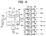
- a solar cell of the present invention having triple cells as three unit devices was produced using a CVD film forming apparatus shown in Fig. 6.
- Fig. 6 there are shown a reaction chamber 600, a substrate 101, an anode 602, a cathode 603, a substrate heater 604, a grounding terminal 605, a matching box 606, a RF power source 607, an exhaust pipe 608, a vacuum pump 609, a film-forming-gas introduction pipe 610, valves 620, 630, 640, 650, 660, 670, 680, 622, 632, 642, 652, 662, 672 and 682, and mass flow controllers 621, 631, 641, 651, 661, 671 and 681.
- a stainless steel (SUS 304) substrate 101 of a size of 5 ⁇ cm with a surface mirror-polished to 0.05 ⁇ m Rmax was charged in an unrepresented sputtering apparatus. After the interior of the apparatus was evacuated to 10 -5 Pa or less, Ar gas was introduced and set to an internal pressure of 0.6 Pa, and a sputtering was executed with an Ag target by generating a DC plasma discharge with a power of 200 W, thereby depositing Ag in a thickness of about 500 nm.
- a sputtering was conducted by changing the target to ZnO but employing the same internal pressure and electric power, thereby depositing ZnO in a thickness of about 500 nm.
- the substrate 101 was taken out and was mounted on the cathode 603 in the reaction chamber 600, and the interior thereof was sufficiently evacuated by the vacuum pump 609 to a vacuum level of 10 -4 Pa measured with an unrepresented ion gauge.
- the substrate 101 was heated to 300°C by the substrate heater 604.
- the valves 620 and 622 were opened and the mass flow controller 621 was so regulated as to introduce SiH 4 gas at a flow rate of 30 sccm, from an unrepresented SiH 4 container into the reaction chamber 600 through the gas introduction pipe 610.
- valves 640 and 642 were opened and the mass flow controller 641 was so regulated as to introduce H 2 gas at a flow rate of 300 sccm
- valves 650 and 652 were opened and the mass flow controller 651 was so regulated as to introduce PH 3 gas diluted to 5 % with H 2 gas at a flow rate of 10 sccm.
- an electric power of 10 W was supplied from the RF power source 607 through the matching box 606, thereby generating a plasma discharge and depositing an n-type amorphous silicon layer 103 in a thickness of 40 nm.
- the interior of the reaction chamber 600 was again evacuated to a vacuum level of 10 -4 Pa or lower, and the valves 620, 622, 630, 632, 640 and 642 were opened to introduce SiH 4 gas at a flow rate of 30 sccm, H 2 gas at a flow rate of 300 sccm and GeH 4 gas at a flow rate of 5.0 sccm into the reaction chamber 600. Then an electric power of 20 W was supplied from the RF power source 607, thereby generating a plasma discharge and depositing an i-type amorphous silicon germanium layer 104 in a thickness of about 180 nm.
- the RF power was turned off to 0 W to terminate the plasma discharge after the termination of the gas supply
- the interior of the reaction chamber 600 was evacuated to a vacuum level of 10 -4 or less, and the valves 620, 622, 640, 642, 660 and 662 were opened to introduce SiH 4 gas at a flow rate of 1 sccm, H 2 gas at a flow rate of 300 sccm and BF 3 gas diluted to 5 % with H 2 gas at a flow rate of 10 sccm into the reaction chamber 600.
- This p-type layer was confirmed to be constituted by microcrystals of a grain size of 2 to 10 nm, by a sample prepared on a glass substrate under the same conditions in a cross-sectional observation under a transmission electron microscope (TEM).
- TEM transmission electron microscope
- an n-type layer 106 was deposited in the same manner as in the formation of the aforementioned n-type 103, and an i-type layer 107 was deposited with a thickness of 100 nm, in the same manner as in the formation of the aforementioned i-type layer 104 except that the flow rate of GeH 4 gas was changed to 2.5 sccm.
- a p-type layer 108 was deposited in the same manner as in the formation of the aforementioned p-type layer 105, but, in the course of film deposition, the valves 670 and 672 were opened and O 2 gas was introduced under such control of the mass flow controller 671 that the oxygen concentration gradually increased toward an interface with an n-type layer 109 to be formed next, thereby completing a middle layer 115.
- O 2 gas was introduced by opening the valves 670 and 672 and regulating the mass flow controller 671.
- the flow rate of O 2 gas was so controlled that the oxygen concentration became continuous with that in the middle p-type layer 108, also had a peak in the vicinity of the interface and gradually decreased thereafter.
- SiH 4 gas at a flow rate of 30 sccm and H 2 gas at a flow rate of 300 sccm were introduced, and an electric power of 20 W was applied to deposit an i-type amorphous silicon layer 110 in a thickness of 70 nm, and a p-type layer 111 was deposited to complete a top layer 116.
- the substrate bearing the formed semiconductor layers was taken out from the reaction chamber 600 and placed in an unrepresented resistance-heated evaporation apparatus.
- the interior of the apparatus was evacuated to 10 -5 Pa or less, oxygen gas was introduced and set to an internal pressure of 50 Pa, and an In-Sn alloy was evaporated by resistance heating, thereby depositing a transparent conductive film (ITO film (indium tin oxide film)) serving as an upper electrode 112 and also having an antireflective function.
- ITO film indium tin oxide film
- the substrate was taken out, then separated into sub cells of a size of 1 cm x 1 cm in an unrepresented dry etching apparatus, and in another evaporation apparatus, an aluminum collecting electrode 113 was formed thereon by electron beam evaporation.
- a solar cell thus obtained is indicated as Sample No. 1-1.
- Samples Nos. 1-2, 1-3, 1-4 and 1-5 were produced in the same manner as explained in the foregoing, except that the O 2 gas flow rate was changed in the middle p-type layer 108 and in the top n-type layer 109.
- Fig. 2 shows a distribution of oxygen concentration in the film thickness direction of these samples, particularly in the vicinity of the interface between the top n-type layer and the middle p-type layer.
- a SIMS measurement was used for determining the oxygen concentration, and confirmed that the oxygen atom concentration had a peak value at a side of the top n-type layer in the vicinity of the n/p interface.
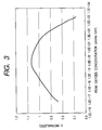
- each sample was irradiated in a solar simulator with a light of solar spectrum of AM-1.5, with an intensity of 100 mW/cm 2 , to obtain a voltage-current curve thereby determining an initial conversion efficiency of the solar cell. Obtained results are shown in Fig. 3.
- Fig. 3 shows an initial conversion efficiency ⁇ as a function of a peak oxygen concentration in the top n-type layer in each sample, in the abscissa.
- the initial conversion efficiency ⁇ is represented in a normalized value, taking the initial conversion efficiency of the sample 1-2 as 1.
- a lower limit of the initial conversion efficiency, preferred for the practical performance and the reliability of the solar cell, is defined as 0.95 in the above-described normalized value. It will be seen that an initial conversion efficiency equal to or higher than such lower limit can be obtained under the condition that a peak oxygen concentration in the vicinity of the p/n interface is within a range from 1 x 10 18 to 1 x 10 22 atoms/cm 3 .
- the film-forming apparatus shown in Fig. 6 was used to produce a triple cell in the same manner as in Example 1, except that O 2 gas used for forming the middle p-type layer and the top n-type layer was changed to CH 4 gas. More specifically, CH 4 gas was supplied by opening the valves 680 and 682 and regulating the mass flow controller 681, and Samples Nos. 2-1, 2-2, 2-3, 2-4 and 2-5 were produced by varying the flow rate.
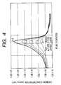
- Fig. 4 shows a distribution of carbon concentration in the film thickness direction of these samples, particularly in the vicinity of the interface between the top n-type layer and the middle p-type layer.
- a SIMS measurement was used for determining the carbon concentration, and confirmed that the carbon atom concentration had a peak value at a side of the middle p-type layer in the vicinity of the p/n interface.
- Fig. 5 shows an initial conversion efficiency ⁇ as a function of a peak carbon concentration in the middle p-type layer in each sample, in the abscissa.
- the initial conversion efficiency ⁇ is represented in a normalized value, taking the initial conversion efficiency of Sample No. 2-2 as 1.
- a lower limit of the initial conversion efficiency is defined as 0.95 in the above-described normalized value. It will be seen that an initial conversion efficiency equal to or higher than such lower limit can be obtained under the condition that a peak carbon concentration in the vicinity of the p/n interface is within a range from 1 x 10 16 to 1 x 10 20 atoms/cm 3 .
- the film-forming apparatus shown in Fig. 6 was used to produce a triple cell in the same manner as in Example 1.
- O 2 gas and CH 4 gas were simultaneously supplied for the middle p-type layer and the top n-type layer. More specifically, O 2 gas and CH 4 gas were supplied by opening the valves 670, 672, 680 and 682 and regulating the mass flow controllers 671 and 681, and samples were produced by varying the flow rate.
- the samples were produced in such a manner that the peak oxygen concentration and the peak carbon concentration were present at the side of the middle p-type layer in the vicinity of the p/n interface, and there was investigated the relationship between the peak oxygen concentration, the peak carbon concentration and the initial conversion efficiency as in Examples 1 and 2. As a result, there were obtained results similar to those in Examples 1 and 2, and it was confirmed that optimum values for the peak oxygen concentration and the peak carbon concentration in the vicinity of the p/n interface were the same as those in Examples 1 and 2.
- the film-forming apparatus shown in Fig. 6 was used to produce a triple cell in the same manner as in Example 1.
- samples were produced in such a manner that the peak oxygen concentration was present at the side of the middle p-type layer in the vicinity of the interface between the middle p-type layer and the top n-type layer, and there was investigated the relationship between the peak oxygen concentration and the initial conversion efficiency with changing the oxygen concentration as in Example 1.
- an optimum value for the peak oxygen concentration in the vicinity of the p/n interface was similar to that in Example 1.
- Production of a photovoltaic device under the aforementioned conditions allows to effectively prevent diffusion of conductive type determining impurities in the p-type semiconductor and/or the n-type semiconductor and to improve the interfacial characteristics. Also, even if the p- or n-conductive type determining impurity is present in an excessive amount, though it deteriorates the photoconductive rate thereby increasing the serial resistance, an addition of oxygen and/or carbon allow to widen a control latitude for the amount of such impurity and also to improve the optical characteristics.
- oxygen and/or carbon allows to form a highly resistant interface, less susceptible to a damage by plasma. It also relaxes a structural strain in the interface, thus improving the matching at the interface, and the adhesion and stability of the films.
- Such improvement in the interfacial characteristics provides a photovoltaic device of a high photoelectric conversion efficiency, and further a photovoltaic device showing an excellent interfacial matching and a high structural stability (film adhesion).
- the present invention provides a photovoltaic device including a plurality of unit devices stacked, each unit device consisting of a silicon-based non-single-crystal semiconductor material and having a pn or pin structure, in which an oxygen atom concentration and/or a carbon atom concentration have maximum peaks in the vicinity of a p/n interface between the plurality of unit devices, thereby stabilizing the p/n interface and improving the interfacial characteristics and the film adhesion to attain a high photoelectric conversion efficiency of the photovoltaic device.
Landscapes
- Photovoltaic Devices (AREA)
Abstract
Description
Claims (6)
- A photovoltaic device comprising a plurality of unit devices stacked, each unit device comprising a silicon-based non-single-crystal semiconductor material and having a pn or pin structure, wherein an oxygen atom concentration has a maximum peak in a vicinity of a p/n interface between the plurality of unit devices.
- A photovoltaic device according to claim 1, wherein a concentration at the peak of the oxygen atom concentration (peak oxygen concentration) is within a range from 1 x 10¹⁸ atoms/cm3 to 1 x 10²² atoms/cm3.
- A photovoltaic device comprising a plurality of unit devices stacked, each unit device comprising a silicon-based non-single-crystal semiconductor material and having a pn or pin structure, wherein a carbon atom concentration has a maximum peak in a vicinity of a p/n interface between the plurality of unit devices.
- A photovoltaic device according to claim 3, wherein a concentration at the peak of the carbon atom concentration (peak carbon concentration) is within a range from 1 x 10¹⁶ atoms/cm3 to 1 x 10²⁰ atoms/cm3.
- A photovoltaic device comprising a plurality of unit devices stacked, each unit device comprising a silicon-based non-single-crystal semiconductor material and having a pn or pin structure, wherein an oxygen atom concentration and a carbon atom concentration have maximum peaks in a vicinity of a p/n interface between the plurality of unit devices.
- A photovoltaic device according to claim 5, wherein a concentration at the peak of the oxygen atom concentration (peak oxygen concentration) is within a range from 1 x 10¹⁸ atoms/cm3 to 1 x 10²² atoms/cm3, and a concentration at the peak of the carbon atom concentration (peak carbon concentration) is within a range from 1 x 10¹⁶ atoms/cm3 to 1 x 10²⁰ atoms/cm3.
Applications Claiming Priority (2)
| Application Number | Priority Date | Filing Date | Title |
|---|---|---|---|
| JP2002166429A JP2004014812A (en) | 2002-06-07 | 2002-06-07 | Photovoltaic element |
| JP2002166429 | 2002-06-07 |
Publications (2)
| Publication Number | Publication Date |
|---|---|
| EP1372198A2 true EP1372198A2 (en) | 2003-12-17 |
| EP1372198A3 EP1372198A3 (en) | 2009-03-04 |
Family
ID=29561712
Family Applications (1)
| Application Number | Title | Priority Date | Filing Date |
|---|---|---|---|
| EP03012797A Withdrawn EP1372198A3 (en) | 2002-06-07 | 2003-06-05 | Photovoltaic device |
Country Status (4)
| Country | Link |
|---|---|
| US (1) | US6911594B2 (en) |
| EP (1) | EP1372198A3 (en) |
| JP (1) | JP2004014812A (en) |
| CN (1) | CN1223013C (en) |
Families Citing this family (25)
| Publication number | Priority date | Publication date | Assignee | Title |
|---|---|---|---|---|
| EP1870944B1 (en) * | 2005-03-24 | 2016-06-01 | Kyocera Corporation | Optoelectric conversion element and its manufacturing method, and optoelectric conversion module using same |
| US20070137699A1 (en) * | 2005-12-16 | 2007-06-21 | General Electric Company | Solar cell and method for fabricating solar cell |
| KR20090042943A (en) * | 2007-02-16 | 2009-05-04 | 미츠비시 쥬고교 가부시키가이샤 | Photoelectric conversion device and manufacturing method thereof |
| US20110017298A1 (en) * | 2007-11-14 | 2011-01-27 | Stion Corporation | Multi-junction solar cell devices |
| KR100876613B1 (en) | 2008-05-27 | 2008-12-31 | 한국철강 주식회사 | Tandem Thin Film Silicon Solar Cell and Manufacturing Method Thereof |
| US20090301562A1 (en) * | 2008-06-05 | 2009-12-10 | Stion Corporation | High efficiency photovoltaic cell and manufacturing method |
| US20110017257A1 (en) * | 2008-08-27 | 2011-01-27 | Stion Corporation | Multi-junction solar module and method for current matching between a plurality of first photovoltaic devices and second photovoltaic devices |
| US20100051090A1 (en) * | 2008-08-28 | 2010-03-04 | Stion Corporation | Four terminal multi-junction thin film photovoltaic device and method |
| US8569613B1 (en) | 2008-09-29 | 2013-10-29 | Stion Corporation | Multi-terminal photovoltaic module including independent cells and related system |
| US8232134B2 (en) | 2008-09-30 | 2012-07-31 | Stion Corporation | Rapid thermal method and device for thin film tandem cell |
| US20100078059A1 (en) * | 2008-09-30 | 2010-04-01 | Stion Corporation | Method and structure for thin film tandem photovoltaic cell |
| JP5180781B2 (en) * | 2008-11-05 | 2013-04-10 | 三菱重工業株式会社 | Method for manufacturing photoelectric conversion device and photoelectric conversion device |
| US8563850B2 (en) * | 2009-03-16 | 2013-10-22 | Stion Corporation | Tandem photovoltaic cell and method using three glass substrate configuration |
| CN102097540A (en) * | 2009-12-11 | 2011-06-15 | 英属开曼群岛商精曜有限公司 | Stack-type solar thin-film cell and manufacture method thereof |
| US20110220177A1 (en) * | 2010-03-10 | 2011-09-15 | United Solar Ovonic Llc | Tandem photovoltaic device with dual function semiconductor layer |
| TWI491066B (en) * | 2010-06-07 | 2015-07-01 | Hon Hai Prec Ind Co Ltd | Light-emitting diode and manufacturing method thereof |
| CN102280551B (en) * | 2010-06-08 | 2015-08-05 | 鸿富锦精密工业(深圳)有限公司 | Light-emitting diode and manufacture method thereof |
| JP2012023342A (en) * | 2010-06-18 | 2012-02-02 | Semiconductor Energy Lab Co Ltd | Photoelectric conversion device and method of producing the same |
| CN102206799B (en) * | 2011-04-20 | 2012-12-19 | 北京大学 | Surface passivation method for germanium-based MOS (Metal Oxide Semiconductor) device substrate |
| JP5824681B2 (en) * | 2011-06-30 | 2015-11-25 | パナソニックIpマネジメント株式会社 | Photovoltaic device |
| JP5919559B2 (en) | 2011-06-30 | 2016-05-18 | パナソニックIpマネジメント株式会社 | Photovoltaic device |
| CN102270691A (en) * | 2011-08-11 | 2011-12-07 | 北京泰富新能源科技有限公司 | Thin-film solar cell |
| CN103346017B (en) * | 2013-07-17 | 2016-11-16 | 重庆大学 | A kind of dye-sensitized solar cell anode and preparation method thereof |
| EP3113224B1 (en) * | 2015-06-12 | 2020-07-08 | Canon Kabushiki Kaisha | Imaging apparatus, method of manufacturing the same, and camera |
| JP6785427B2 (en) | 2016-02-01 | 2020-11-18 | パナソニックIpマネジメント株式会社 | Solar cell elements and solar cell modules |
Family Cites Families (13)
| Publication number | Priority date | Publication date | Assignee | Title |
|---|---|---|---|---|
| US2949498A (en) | 1955-10-31 | 1960-08-16 | Texas Instruments Inc | Solar energy converter |
| US2948498A (en) * | 1956-10-04 | 1960-08-09 | Trane Co | Roll-out mechanism |
| US4776894A (en) * | 1986-08-18 | 1988-10-11 | Sanyo Electric Co., Ltd. | Photovoltaic device |
| US4891330A (en) * | 1987-07-27 | 1990-01-02 | Energy Conversion Devices, Inc. | Method of fabricating n-type and p-type microcrystalline semiconductor alloy material including band gap widening elements |
| DE69326878T2 (en) | 1992-12-14 | 2000-04-27 | Canon K.K., Tokio/Tokyo | Photosensitive element with a multilayered layer with increased hydrogen and / or halogen atom concentration in the interface region of adjacent layers |
| JP2984537B2 (en) * | 1994-03-25 | 1999-11-29 | キヤノン株式会社 | Photovoltaic element |
| JP2733471B2 (en) | 1996-02-05 | 1998-03-30 | 株式会社半導体エネルギー研究所 | Semiconductor device |
| JP3294097B2 (en) | 1996-02-14 | 2002-06-17 | 三菱重工業株式会社 | Amorphous semiconductor solar cell |
| JP2000138384A (en) | 1998-10-30 | 2000-05-16 | Sanyo Electric Co Ltd | Amorphous semiconductor device and its manufacture |
| JP3589581B2 (en) | 1999-02-26 | 2004-11-17 | 株式会社カネカ | Manufacturing method of tandem type thin film photoelectric conversion device |
| EP1056139A3 (en) * | 1999-05-28 | 2007-09-19 | Sharp Kabushiki Kaisha | Method for manufacturing photoelectric conversion device |
| US6614506B2 (en) * | 2000-05-31 | 2003-09-02 | Canon Kabushiki Kaisha | Image forming apparatus and registration correcting method of the image forming apparatus |
| JP4560245B2 (en) | 2001-06-29 | 2010-10-13 | キヤノン株式会社 | Photovoltaic element |
-
2002
- 2002-06-07 JP JP2002166429A patent/JP2004014812A/en active Pending
-
2003
- 2003-06-02 US US10/449,104 patent/US6911594B2/en not_active Expired - Fee Related
- 2003-06-05 EP EP03012797A patent/EP1372198A3/en not_active Withdrawn
- 2003-06-06 CN CNB031412149A patent/CN1223013C/en not_active Expired - Fee Related
Also Published As
| Publication number | Publication date |
|---|---|
| US6911594B2 (en) | 2005-06-28 |
| US20030227017A1 (en) | 2003-12-11 |
| CN1223013C (en) | 2005-10-12 |
| CN1469494A (en) | 2004-01-21 |
| JP2004014812A (en) | 2004-01-15 |
| EP1372198A3 (en) | 2009-03-04 |
Similar Documents
| Publication | Publication Date | Title |
|---|---|---|
| US6911594B2 (en) | Photovoltaic device | |
| US6700057B2 (en) | Photovoltaic device | |
| KR100251070B1 (en) | Photovoltaic device | |
| US5279679A (en) | Multi-layered photovoltaic element having at least three unit cells | |
| AU734676B2 (en) | Photovoltaic element and method of producing same | |
| US5913986A (en) | Photovoltaic element having a specific doped layer | |
| JP4208281B2 (en) | Multilayer photovoltaic device | |
| JP2951146B2 (en) | Photovoltaic devices | |
| JP2719230B2 (en) | Photovoltaic element | |
| US20070023081A1 (en) | Compositionally-graded photovoltaic device and fabrication method, and related articles | |
| JP2918345B2 (en) | Photovoltaic element | |
| JP2845383B2 (en) | Photovoltaic element | |
| JP2007189266A (en) | Stacked photovoltaic device | |
| JP2710246B2 (en) | Photovoltaic element | |
| JPH09191119A (en) | Method for manufacturing photovoltaic element | |
| JP2013012593A (en) | Thin film photoelectric conversion device |
Legal Events
| Date | Code | Title | Description |
|---|---|---|---|
| PUAI | Public reference made under article 153(3) epc to a published international application that has entered the european phase |
Free format text: ORIGINAL CODE: 0009012 |
|
| AK | Designated contracting states |
Kind code of ref document: A2 Designated state(s): AT BE BG CH CY CZ DE DK EE ES FI FR GB GR HU IE IT LI LU MC NL PT RO SE SI SK TR |
|
| AX | Request for extension of the european patent |
Extension state: AL LT LV MK |
|
| PUAL | Search report despatched |
Free format text: ORIGINAL CODE: 0009013 |
|
| AK | Designated contracting states |
Kind code of ref document: A3 Designated state(s): AT BE BG CH CY CZ DE DK EE ES FI FR GB GR HU IE IT LI LU MC NL PT RO SE SI SK TR |
|
| AX | Request for extension of the european patent |
Extension state: AL LT LV MK |
|
| 17Q | First examination report despatched |
Effective date: 20090924 |
|
| 17P | Request for examination filed |
Effective date: 20090904 |
|
| AKX | Designation fees paid |
Designated state(s): AT BE BG CH CY CZ DE DK EE ES FI FR GB GR HU IE IT LI LU MC NL PT RO SE SI SK TR |
|
| 18W | Application withdrawn |
Effective date: 20100128 |
|
| STAA | Information on the status of an ep patent application or granted ep patent |
Free format text: STATUS: THE APPLICATION HAS BEEN WITHDRAWN |
|
| R18W | Application withdrawn (corrected) |
Effective date: 20100128 |