EP1372156A2 - Data output driver and data output method for minimizing data output time variations caused by data patterns - Google Patents
Data output driver and data output method for minimizing data output time variations caused by data patterns Download PDFInfo
- Publication number
- EP1372156A2 EP1372156A2 EP03253634A EP03253634A EP1372156A2 EP 1372156 A2 EP1372156 A2 EP 1372156A2 EP 03253634 A EP03253634 A EP 03253634A EP 03253634 A EP03253634 A EP 03253634A EP 1372156 A2 EP1372156 A2 EP 1372156A2
- Authority
- EP
- European Patent Office
- Prior art keywords
- intermediate node
- data
- input
- voltage
- terminal
- Prior art date
- Legal status (The legal status is an assumption and is not a legal conclusion. Google has not performed a legal analysis and makes no representation as to the accuracy of the status listed.)
- Granted
Links
Images


Classifications
-
- G—PHYSICS
- G11—INFORMATION STORAGE
- G11C—STATIC STORES
- G11C11/00—Digital stores characterised by the use of particular electric or magnetic storage elements; Storage elements therefor
- G11C11/21—Digital stores characterised by the use of particular electric or magnetic storage elements; Storage elements therefor using electric elements
- G11C11/34—Digital stores characterised by the use of particular electric or magnetic storage elements; Storage elements therefor using electric elements using semiconductor devices
- G11C11/40—Digital stores characterised by the use of particular electric or magnetic storage elements; Storage elements therefor using electric elements using semiconductor devices using transistors
- G11C11/401—Digital stores characterised by the use of particular electric or magnetic storage elements; Storage elements therefor using electric elements using semiconductor devices using transistors forming cells needing refreshing or charge regeneration, i.e. dynamic cells
- G11C11/4063—Auxiliary circuits, e.g. for addressing, decoding, driving, writing, sensing or timing
- G11C11/407—Auxiliary circuits, e.g. for addressing, decoding, driving, writing, sensing or timing for memory cells of the field-effect type
- G11C11/409—Read-write [R-W] circuits
- G11C11/4096—Input/output [I/O] data management or control circuits, e.g. reading or writing circuits, I/O drivers or bit-line switches
-
- G—PHYSICS
- G11—INFORMATION STORAGE
- G11C—STATIC STORES
- G11C7/00—Arrangements for writing information into, or reading information out from, a digital store
- G11C7/10—Input/output [I/O] data interface arrangements, e.g. I/O data control circuits, I/O data buffers
- G11C7/1051—Data output circuits, e.g. read-out amplifiers, data output buffers, data output registers, data output level conversion circuits
- G11C7/1057—Data output buffers, e.g. comprising level conversion circuits, circuits for adapting load
-
- G—PHYSICS
- G11—INFORMATION STORAGE
- G11C—STATIC STORES
- G11C7/00—Arrangements for writing information into, or reading information out from, a digital store
- G11C7/10—Input/output [I/O] data interface arrangements, e.g. I/O data control circuits, I/O data buffers
- G11C7/1051—Data output circuits, e.g. read-out amplifiers, data output buffers, data output registers, data output level conversion circuits
Definitions
- the present invention relates to a semiconductor memory device, and more particularly, to a data output driver and data output method for minimizing data output time (tQ) variation caused by various data patterns.
- tQ data output time
- SDRAM synchronous dynamic random access memory
- DDR dual data rate
- RAMBUS® DRAM input or output data synchronized both at the rising edge and the falling edge of a system clock.
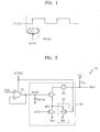
- FIG. 1 is a timing diagram showing variations in data output time (tQ).
- the output time (tQ) of each data item through a plurality of input and/or output pads synchronized to a system clock (CLOCK) is almost constant.
- RAMBUS® DRAMs semiconductor device manufacturers test the data output time (tQ) through input and/or output pads according to predetermined specifications, and RAMBUS® DRAMs that do not satisfy the specifications are treated as poor quality products. As a result, the yield of semiconductor chips may decrease.
- a data output driver adapted to drive data that is input through an input terminal, to an output terminal, comprising: an intermediate node; a first driver connected between the output terminal and the intermediate node, the first driver having a control terminal and being adapted to provide a current path between the intermediate node and the output terminal in response to an enable signal input to the control terminal; a second driver connected between the intermediate node and a lower supply voltage (e.g., ground) and being adapted to drive the data that is input to the input terminal to the output terminal through the intermediate node in a data read operation; and a voltage control circuit connected between the intermediate node and the lower supply voltage, wherein the voltage control circuit has a control terminal and is adapted to cause at least a portion of the current of the intermediate node to flow to the lower supply voltage in response to a control signal input to the control terminal.
- the voltage control circuit is adapted to maintain a voltage swing at the intermediate node at a substantially constant level during the data read operation.
- a data output driver having an input terminal and an output terminal, comprising: a first current path provided between the output terminal and an intermediate node when a data read operation is performed; a driver adapted to drive data that is input through the input terminal, to the output terminal through the intermediate node in the data read operation; and a second current path provided between the intermediate node and a lower supply voltage (e.g., ground) during the data read operation.
- a lower supply voltage e.g., ground
- the second current path causes a portion of a charging current, that flows into the intermediate node through the first current path, to flow into the lower supply voltage.
- a data output driver adapted to drive data that is input through an input terminal, to an output terminal, comprising: an intermediate node; a first transistor connected between the output terminal and the intermediate node, the first transistor including a control terminal to which an enable signal is input; a second transistor connected between the intermediate node and a lower supply voltage (e.g., ground), the second transistor including the input terminal through which the data is input; and a third transistor connected between the intermediate node and the lower supply voltage, the third transistor including a control terminal to which a control signal is input.
- the enable signal is activated when the data output driver performs a data read operation.
- the control signal is activated when the data output driver performs a data read operation.
- the third transistor discharges to the lower supply voltage a portion of a current flowing into the intermediate node, to maintain a voltage swing at the intermediate node at a substantially constant level.
- the first through the third transistors are NMOS transistors.
- a data output driver comprising: an output terminal; an intermediate node; a first transistor connected between the output terminal and the intermediate node, and including a gate to which an enable signal is input; a second transistor connected between the intermediate node and a lower supply voltage (e.g., ground), and including a gate to which data is input; and a third transistor connected between the intermediate node and the lower supply voltage, and comprising a gate to which a control signal is input.
- the third transistor causes a predetermined amount of a current flowing into the intermediate node through the first transistor to flow to the lower supply voltage, maintaining a voltage swing at the intermediate node at a substantially constant level during the data read operation.
- a method of outputting data that is input to an input terminal of a data output driver to an output terminal of the data output driver, the data output driver having an intermediate node comprising: maintaining a voltage swing at the intermediate node at a substantially constant level during a data read operation; and outputting the data which is input through the input terminal, to the output terminal through the intermediate node.
- Maintaining a voltage swing voltage at the intermediate node at a substantially constant level during a data read operation may beneficially comprise providing a current path between the intermediate node and a lower supply voltage (e.g., ground) to maintain a voltage swing voltage at the intermediate node at a substantially constant level during a data read operation.
- a lower supply voltage e.g., ground
- a semiconductor memory device comprising a plurality of data output drivers for outputting data that are input through respective input terminals, to respective output terminals, wherein each of the plurality of data output drivers comprises: an intermediate node; a first transistor connected between one of the output terminals and the intermediate node, and including a gate to which an enable signal is input; a second transistor connected between the intermediate node and a lower supply voltage, and including a gate to which one of the plural data is input; and a third transistor connected between the intermediate node and the lower supply voltage, and comprising a gate to which a control signal is input.
- the third transistor causes a predetermined amount of a current flowing into the intermediate node through the first transistor to flow to the lower supply voltage, maintaining a voltage swing at the intermediate node at a substantially constant level during the data read operation.
- a data output driver having an input terminal and an output terminal, comprising: an intermediate node; a first transistor connected between the output terminal and the intermediate node, the first transistor including a control terminal to which an enable signal is input; a second transistor connected between the intermediate node and a lower supply voltage, the second transistor adapted to discharge to the lower supply voltage a first current quantity according to data that is input to the input terminal; and a third transistor connected between the intermediate node and the lower supply voltage, the second transistor including a control terminal and being adapted to discharge to the lower supply voltage a second current quantity according to a control signal that is input to the control terminal thereof.
- the present invention thus provides a data output driver and data output method that minimizes data output time (tQ) variations caused by data patterns that are input.
- FIG. 2 is a block diagram of a semiconductor device having an open-drain output driver according to a first embodiment.
- the semiconductor device 10 comprises an enable signal generating circuit 20 and an open-drain output driver 30.
- a terminating resistor (Rtt) is connected between a terminating voltage (Vtt) and an output terminal 35.
- the open-drain output driver 30 is an example of a data output driver.
- the semiconductor device 10 includes a capacitor (Cenvg) between the gate of a first NMOS transistor 31 and a lower supply voltage (VSS) (e.g., ground).
- the capacitor (Cenvg) removes coupling voltage or coupling noise that is provided to the gate of a first NMOS transistor 31. Coupling voltage or coupling noise adversely affects the characteristics of an output signal. Therefore, it is beneficial that the capacitance of the capacitor (Cenvg) be substantially large.
- the open-drain output driver 30 Whether the open-drain output driver 30 operates or not, the output resistance of the open-drain output driver 30 is high. Therefore, with its advantage in channel impedance matching and other advantages, the open-drain output driver 30 is essentially used in the RAMBUS® DRAMs, and also is widely used in chip-to-chip connection systems.
- the enable signal generating circuit 20 is implemented by a comparator, whose (+) input terminal receives a predetermined voltage, and whose (-) input terminal is connected to the output terminal of the comparator 20.
- the enable signal generating circuit 20 compares the predetermined voltage (ENV) which is input to the (+) input terminal, with the voltage which is input to the (-) input terminal, and outputs an enable signal (ENVG), the result of the comparison, to the gate of the first NMOS transistor 31.
- the enable signal (ENVG) swings between the lower supply voltage (VSS) (e.g., ground) level and a first voltage level.
- the enable signal generating circuit 20 outputs an enable signal (ENVG) having the lower supply voltage (VSS) (e.g., ground) level to the gate of the first NMOS transistor 31. If the semiconductor device 10 performs a data read operation, the enable signal generating circuit 20 outputs an enable signal (ENVG) having the first voltage level to the gate of the NMOS transistor 31.
- VSS lower supply voltage
- the first NMOS transistor 31 operates in a saturation region in response to the first voltage level. If the first NMOS transistor 31 operates in a saturation region, the output resistance value of the open-drain output driver 30 is kept substantially high.
- the open-drain output driver 30 comprises a first driver (implemented by the first NMOS transistor 31), a second driver implemented by a second NMOS transistor 33, the output terminal 35, and a voltage control circuit 37.
- the second NMOS transistor is connected between an intermediate node (MID) and ground (VSS), and drives data (DATA), which is input to the gate of the second NMOS transistor 33, to the output terminal 35 through the intermediate node (MID).
- the data (DATA) that is input to the gate of the second NMOS transistor 33 has a voltage level that is either near or at lower power supply voltage (VSS) (e.g., ground) (logic "0"), or near or at an upper power supply voltage (logic "1").
- VSS lower power supply voltage
- upper power supply voltage logic "1”
- all power supply levels including for example 3.3V, 2.5V, or 1.8V, can be used.
- the first NMOS transistor 31 is connected between the output terminal 35 and the intermediate node (MID).
- the enable signal (ENVG) is input to the gate of the first NMOS transistor 31.
- the enable signal (ENVG) is constant regardless of changes of coupling voltage (noise), voltage, temperature and process variations.
- the voltage control circuit 37 is implemented by the third NMOS transistor 39, and is connected between the intermediate node (MID) and ground (VSS).
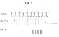
- a control signal (ACTIVE) is input to the gate of the third NMOS transistor 39. That is, in response to the control signal (ACTIVE) being activated (for example, in a logic "high” state) the voltage control circuit 37 maintains the intermediate node (MID) at a constant voltage.
- FIG. 3 is a timing diagram of a data read operation of the semiconductor device 10 shown in FIG. 2. Referring to FIGS. 2 and 3, the operation of the semiconductor device 10 having the open-drain output driver 30 will now be explained in detail.
- the enable signal generating circuit 20 outputs an enable signal (ENVG) having the lower supply voltage (VSS) (e.g., ground) level to the gate of the first NMOS transistor 31.
- VSS lower supply voltage
- the open-drain output driver 30 is off.
- the first NMOS transistor 31 of the semiconductor device 10 may be off or on.
- the enable signal generating circuit 20 outputs the enable signal (ENVG) having the first voltage level to the gate of the first NMOS transistor 31.
- the first NMOS transistor 31 operates in a saturation region and a first current path is formed between the output terminal 35 and the intermediate node (MID).
- the voltage of the output terminal 35 is determined according to the data (DATA) applied to the gate of the second NMOS transistor 33, and in this manner, the open-drain output driver 30 can perform a data read operation.
- the second NMOS transistor 33 is turned on. Accordingly, a current is discharged from the terminating power source (V TT ) to ground (VSS), and the voltage at the output terminal 35 is determined by the ratio of the terminating resistance (R TT ) to the turn-on resistance of transistors 31, 33, and 39.
- the second NMOS transistor 33 is turned off. Accordingly, the first current path from the terminating power source (V TT ) to the intermediate node (MID) is formed and the intermediate node (MID) is charged.
- the voltage that is output from the output terminal 35 has the level of the terminating power source (V TT ).
- the second current path causes some current which is flowing into the intermediate node (MID) through the first NMOS transistor 31 and charges the intermediate node (MID) (hereinafter, referred to as a "charging current") to flow to ground (VSS). Accordingly, the voltage (VMID) of the intermediate node (MID) is kept substantially constant by the presence of the second current path.
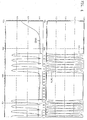
- FIG. 4 is a timing diagram of an input and/or output waveform of the open-drain output driver shown in FIG. 2.
- the output voltage (V OUT ) and data (DATA) swing between1.0V and 1.8V
- the voltage (VMID) of the intermediate node (MID) swings between 0.1V and 0.62V.
- the swing widths of the output voltage (VOUT), data, and the voltage (VMID) of the intermediate node (MID) may vary in a variety of ways according to the design of a semiconductor device.
- a data read operation if initial data is read, or if input data (DATA) having a logic value of "0" is continuously input to the gates of a plurality of the second NMOS transistors 33, the charging current flowing into the intermediate node (MID) through the first NMOS transistor 31 tends to cause the voltage (VMID) of the intermediate node (MID) to slowly rise from a voltage obtained by subtracting a threshold voltage of the first NMOS transistor 31 from the first voltage level.
- the third NMOS transistor 39 of the open-drain output driver 10 causes some of the charging current flowing into the intermediate node (MID) to flow to the lower supply voltage (VSS) (e.g., ground) through the second current path, the voltage (VMID) of the intermediate node (MID) is kept constant.
- VSS lower supply voltage
- the third NMOS transistor 39 discharges the charging current flowing into the intermediate node (MID), to ground (VSS), the voltage (VMID) of the intermediate node (MID) is kept constant.
- the open-drain output driver 30 can maintain the data output time (tQ) of data having a logic value of "1", regardless of input data patterns, for example, 01, 0001, or 00001.
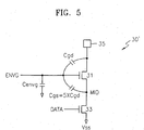
- FIG. 5 is a diagram of an equivalent circuit of an open-drain output driver having no current path. That is, FIG. 5 shows a coupling environment of the open-drain output driver 10 shown in FIG. 2.
- a parasitic capacitor (Cgd) is formed between the gate and drain of the first NMOS transistor 31, and a parasitic capacitor (Cgs) is formed between the gate and source of the first NMOS transistor 31.
- the capacitance of the parasitic capacitor (Cgs) is about five times larger than that of the parasitic capacitor (Cgd).
- the ratio of the capacitance of the parasitic capacitor (Cgs) and the capacitance of the parasitic capacitor (Cgd) may be implemented with a variety of values.
- the structures and functions of the first driver 31 and the second driver 33 of the open-drain output driver 30' are the same as the structures and functions of the first driver 31 and the second driver 33 of the open-drain output driver 30 of FIG. 2.
- the open-drain output driver 30' does not include the NMOS transistor 39 of FIG. 2.
- the swing width of the output voltage (Vout) of the output terminal 35 is about 800mV
- the swing width of the voltage (VMID) of the intermediate node (MID) is about 500mV.
- the variations in the output voltage (Vout) of the output terminal 35 and the voltage (VMID) of the intermediate node (MID) are coupled to the gate of the first NMOS transistor 31 by respective parasitic capacitors (Cgd, and Cgs) of the first NMOS transistor 31.
- dVout denotes variation of the output voltage of the output terminal 35
- dVMID denotes variation of the voltage of the intermediate node (MID).
- dVout is 800mV and dVMID is 500mV.
- the coupling voltage (C_ENVG) is a noise voltage induced to the gate of the first NMOS transistor 31 by the voltage of the output terminal 35 or the voltage (VMID) of the intermediate node (MID) through respective parasitic capacitors (Cgd, and Cgs).
- the coupling voltage (C_ENVG) is proportional to the product of the voltage variations (dVout, dVMID) and the capacitance of the respective parasitic capacitors (Cgd, and Cgs). Since the capacitance of the capacitor (Cgs) is substantially larger than that of the capacitor (Cgd) in general, most of the coupling voltage (C_ENVG) is induced to the gate of the first NMOS transistor 31 by the voltage variation of the intermediate node (MID).
- the coupling voltage (C_ENVG) is, the better the memory device is.
- the coupling voltage (C_ENVG) is maintained at a constant level if it is actually impossible to remove the coupling voltage (C_ENVG) completely.
- the coupling by the capacitor (Cgd) is held constant by the output voltage (Vout) always swinging 800mV, but the coupling by the capacitor (Cgs) can vary according to the voltage (VMID) of the intermediate node (MID).
- the voltage variation (dVMID) of the intermediate node (MID) affects the coupling voltage (C_ENVG)
- the driving capability of the first NMOS transistor 31, which operates in a saturation region in response to an enable signal (ENVG) is affected by the voltage variation (dVMID), and as a result, the data output time (tQ) changes according to the pattern of the data (DATA) which is input to the gate of the second NMOS transistor 33.
- the third NMOS transistor 39 of the open-drain output driver 30 shown in FIG. 2 minimizes the variation of the voltage (VMID) of the intermediate node (MID) caused by the pattern of data (DATA) that is input to the gate of the second NMOS transistor 33 such that the variation of the data output time (tQ) is minimized.
- the open-drain output driver 10 of FIG. 2 minimizes the variation of the data output time (tQ) regardless of the pattern of data (DATA) that is input to the gate of the second NMOS transistor 33.
- FIG. 6 is a timing diagram showing an enable signal of an open-drain output driver and a voltage waveform of an intermediate node according to a first data pattern.
- FIG. 7 is a timing diagram showing an enable signal of an open-drain output driver and a voltage waveform of an intermediate node according to a second data pattern.
- the current driving capability of the first NMOS transistor 31 decreases, and a time increases for discharging the voltage (VMID') of the intermediate node (MID) to the level when data is read having a logic value of "1" (for example, 0.1V).
- the third NMOS transistor 39 of the open-drain output driver 10 discharges some the charging current flowing into the intermediate node (MID) to the lower supply voltage (VSS) (e.g., ground) in the response to the control signal (ACTIVE), the voltage (VMID) of the intermediate node (MID) is maintained at or near a constant level.
- VSS lower supply voltage
- ACTIVE control signal
- FIG. 8 is a timing diagram showing an enable signal of an open-drain output driver and a voltage waveform of an intermediate node according to a third data pattern.
- the third NMOS transistor 39 discharges some the charging current flowing into the intermediate node (MID) to lower supply voltage (VSS) (e.g., ground) in response to the control signal (ACTIVE), the voltage (VMID) of the intermediate node (MID) is maintained at or near a constant level.
- VSS supply voltage
- ACTIVE control signal
- the open-drain output driver 30 as disclosed herein substantially reduces the variation of the output time (tQ) of data "1" in a data read operation even when data patterns that are input to the gate of the second NMOS transistor 33 are 01, 001, 0001, 0001, and 000001, etc., for example,.
- FIG. 9 is a timing diagram of an input and/or output waveform of the open-drain output driver shown in FIG. 5.
- the voltage (VMID') of the intermediate node (MID) of the open-drain output driver 30' of FIG. 5 is different when data is initially read than it is in an interval "AA" where a continuous string of logic "0s" is input.
- the voltage (VMID') of the intermediate node (MID) rises up to about 0.9V.
- the voltage (VMID') of the intermediate node (MID) only rises up to about 0.76V. In other intervals, the voltage (VMID') of the intermediate node (MID) rises up to about 0.68V.
- the coupling voltage (C_ENVG) of the equation 1 coupled to the gate of the first NMOS transistor 31 varies according to the pattern of data input to the gate of the second NMOS transistor 33 and, as a result, the data output time (tQ) varies according to the data patterns.
- the open-drain output driver 30 as disclosed herein maintains a constant voltage variation (dVMID) of the intermediate node regardless of the data patterns input to the gate of the second NMOS transistor 33. Accordingly, the variation of the data output time (tQ) is substantially minimized.
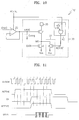
- FIG. 10 is a block diagram of a semiconductor device having an open-drain output driver according to a second embodiment.
- the semiconductor device 10' comprises an enable signal generating circuit 20 and an open-drain output driver 50.
- the open-drain output driver 50 comprises a first driver 31, a second driver 33, an output terminal 35, a voltage control circuit 37, and an enable interval control circuit 40.
- the second driver 33 is implemented by a second NMOS transistor connected between an intermediate node (MID) and ground (VSS), and drives data (DATA) that is input to the gate of the second NMOS transistor 33 to the output terminal 35 through the intermediate node (MID).
- the first driver 31 is implemented by a first NMOS transistor, and is connected between the output terminal 35 and the intermediate terminal (MID).
- An enable signal (ENVG) is input to the gate of the first NMOS transistor 31.
- FIG. 11 is a timing diagram of a data read operation of the semiconductor device shown in FIG. 10.
- the voltage control circuit 37 is implemented by the third NMOS transistor 39, and is connected between the intermediate node (MID) and ground (VSS).
- the first control signal (ACTIVE') is input to the gate of the third NMOS transistor 39.
- the enable interval control circuit 40 comprises a buffer and an AND gate, and controls activated intervals of the first control signal (ACTIVE') by performing an AND operation of the control signal (ACTIVE) and the output signal (D1) of the buffer.
- an activated interval of the first control signal (ACTIVE') is activated at least one cycle before data (DATA) is input, and is inactivated at least one cycle after data (DATA) are all read.
- the third NMOS transistor 39 is turned on in response to the first control signal (ACTIVE') such that when the voltage of the data (DATA) is input to the gate of the NMOS transistor 33, the rise of the voltage (VMID) caused by variations in data patterns, processes, voltage, and temperature, etc. is prevented.
- the third NMOS transistor 39 discharges some of the charging current flowing into the intermediate node (MID) so that the voltage (VMID) of the intermediate node (MID) is maintained at or near a constant level.
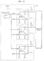
- FIG. 12 is a block diagram of a semiconductor device having an open-drain output driver according to a third embodiment.
- the semiconductor device 100 comprises an enable signal generating circuit 20 and a plurality of data output drivers 10_1 through 10_n. It is preferable that each of the plurality of data output drivers 10_1 through 10_n is an open-driver output driver.
- the structures and functions of the enable signal generating circuit 20 of FIG. 12 are the same as the structures and functions of the enable signal generating circuits 20 of FIG. 2. That is, when the semiconductor device 100 is in a stand-by state, the enable signal generating circuit 20 outputs an enable signal (ENVG) having the lower supply voltage (VSS) (e.g., ground) level to the gate of each transistor 31_1 through 31_n.
- ENVG enable signal
- VSS lower supply voltage
- the enable signal generating circuit 20 When the semiconductor device 100 performs a data read operation, the enable signal generating circuit 20 outputs an enable signal (ENVG) having the first voltage level to the gate of each transistor 31_1 through 31_n. Accordingly, in response to the enable signal (ENVG), each transistor 31_1 through 31_n operates in a saturation region.
- ENVG enable signal
- the structures and functions of the open-drain output drivers 10_1 through 10_n are the same as the structure and function of any of the open-drain output drivers 10 and 10' shown in FIGS. 2 and 10.
- Open-drain output drivers 10_1 through 10_n each drive data (DATA1 through DATAN), which are input through input terminals, to respective output terminals.
- Terminating resistors (RTTs) are connected between the terminating voltage (VTT) and respective output terminals 35_1 through 35_n.
- Transistors 39_1 through 39_n are each connected between respective intermediate nodes (MID_1 through MID_n) and the ground (VSS). Transistors 39_1 through 39_n each discharge some of the charging current flowing into the respective intermediate nodes (MID_1 through MID_n) through respective transistors 31_1 through 31_n, to the lower supply voltage (VSS) (e.g., ground) so that respective intermediate nodes (MID_1 through MID_n) are maintained at a constant voltage level. Accordingly, the coupling voltage (C_ENVG) which is expressed by the equation 1 and is coupled to the gate of each transistor 31_1 through 31_n also decreases.
- VSS lower supply voltage
- each transistor 39_1 through 39_n When the semiconductor device 100 performs a data read operation, the current consumed by each transistor 39_1 through 39_n is quite small, for example, 1/180 of the current consumed in a data read operation. Accordingly, the voltage drop of each output terminal 35_1 through 35_n caused by each transistor 39_1 through 39_n is on the order of millivolts (mV).
- the plurality of open-drain output drivers 10_1 through 10_n minimize variation of respective data output times (tQ) caused by data patterns input to respective input terminals 33_1 through 33_n.
- the open-drain output driver and data output method as discussed herein can minimize the variation of the data output time (tQ) caused by data patterns input to the input terminal. As a result, the open-drain output driver and data output method can transmit data at a high speed.
Landscapes
- Engineering & Computer Science (AREA)
- Databases & Information Systems (AREA)
- Microelectronics & Electronic Packaging (AREA)
- Computer Hardware Design (AREA)
- Logic Circuits (AREA)
- Dram (AREA)
Abstract
Description
Referring to FIGS. 5 and 9, the voltage (VMID') of the intermediate node (MID) of the open-drain output driver 30' of FIG. 5 is different when data is initially read than it is in an interval "AA" where a continuous string of logic "0s" is input. Before data is initially read, the voltage (VMID') of the intermediate node (MID) rises up to about 0.9V. In contrast, in the interval "A," the voltage (VMID') of the intermediate node (MID) only rises up to about 0.76V. In other intervals, the voltage (VMID') of the intermediate node (MID) rises up to about 0.68V.
Claims (18)
- A data output driver adapted to drive data that is input through an input terminal, to an output terminal, comprising:an intermediate node;a first driver connected between the output terminal and the intermediate node, the first driver having a control terminal and being adapted to provide a current path between the intermediate node and the output terminal in response to an enable signal input to the control terminal;a second driver connected between the intermediate node and a lower supply voltage and being adapted to drive the data that is input to the input terminal to the output terminal through the intermediate node in a data read operation; anda voltage control circuit connected between the intermediate node and the lower supply voltage, wherein the voltage control circuit has a control terminal and is adapted to cause at least a portion of the current of the intermediate node to flow to the lower supply voltage in response to a control signal input to the control terminal.
- The data output driver of claim 1, wherein the voltage control circuit is adapted to maintain a voltage swing at the intermediate node at a substantially constant level during the data read operation.
- The data output driver of claim 1 or 2, wherein the current driving capability of the voltage control circuit is less than the current driving capability of the first driver.
- A data output driver having an input terminal and an output terminal, comprising:a first current path provided between the output terminal and an intermediate node when a data read operation is performed;a driver adapted to drive data that is input through the input terminal, to the output terminal through the intermediate node in the data read operation; anda second current path provided between the intermediate node and a lower supply voltage during the data read operation.
- The data output driver of claim 4, wherein the second current path causes a portion of a charging current, that flows into the intermediate node through the first current path, to flow into the lower supply voltage.
- A data output driver adapted to drive data that is input through an input terminal, to an output terminal, comprising:an intermediate node;a first transistor connected between the output terminal and the intermediate node, the first transistor including a control terminal to which an enable signal is input;a second transistor connected between the intermediate node and a lower supply voltage, the second transistor including the input terminal through which the data is input; anda third transistor connected between the intermediate node and the lower supply voltage, the third transistor including a control terminal to which a control signal is input.
- The data output driver of claim 6, wherein the enable signal is activated when the data output driver performs a data read operation.
- The data output driver of claim 6, wherein the control signal is activated when the data output driver performs a data read operation.
- The data output driver of claim 6, wherein when the data output driver performs a data read operation, the third transistor discharges to the lower supply voltage a portion of a current flowing into the intermediate node, to maintain a voltage swing at the intermediate node at a substantially constant level during the data read operation.
- The data output driver of any one of claims 6 to 9, wherein the first through the third transistors are NMOS transistors.
- A data output driver comprising:an output terminal;an intermediate node;a first transistor connected between the output terminal and the intermediate node, and including a gate to which an enable signal is input;a second transistor connected between the intermediate node and a lower supply voltage, and including a gate to which data is input; anda third transistor connected between the intermediate node and the lower supply voltage, and comprising a gate to which a control signal is input.
- The data output driver of claim 11, wherein when the data output driver performs a data read operation, the third transistor causes a predetermined amount of a current flowing into the intermediate node through the first transistor to flow to the lower supply voltage, maintaining a voltage swing at the intermediate node at a substantially constant level during the data read operation.
- A method of outputting data that is input to an input terminal of a data output driver to an output terminal of the data output driver, the data output driver having an intermediate node, the method comprising:maintaining a voltage swing at the intermediate node at a substantially constant level during a data read operation; andoutputting the data which is input through the input terminal, to the output terminal through the intermediate node.
- The method of claim 13, wherein maintaining a voltage swing at the intermediate node at a substantially constant level during a data read operation comprises providing a current path between the intermediate node and a lower supply voltage to maintain a voltage swing voltage at the intermediate node at a substantially constant level during a data read operation.
- The method of claim 14, wherein the current path is provided between the intermediate node and the lower supply voltage in response to a data read signal, said current path causing a portion of a charging current, flowing into the intermediate node, to flow to the lower supply voltage.
- A semiconductor memory device comprising a plurality of data output drivers for outputting data that are input through respective input terminals, to respective output terminals, wherein each of the plurality of data output drivers comprises:an intermediate node;a first transistor connected between one of the output terminals and the intermediate node, and including a gate to which an enable signal is input;a second transistor connected between the intermediate node and a lower supply voltage, and including a gate to which one of the plural data is input; anda third transistor connected between the intermediate node and the lower supply voltage, and comprising a gate to which a control signal is input.
- The semiconductor memory device of claim 16, wherein when the semiconductor memory device performs a data read operation, the third transistor causes a predetermined amount of a current flowing into the intermediate node through the first transistor to flow to the lower supply voltage, maintaining a voltage swing at the intermediate node at a substantially constant level during the data read operation.
- A data output driver having an input terminal and an output terminal, comprising:an intermediate node;a first transistor connected between the output terminal and the intermediate node, the first transistor including a control terminal to which an enable signal is input;a second transistor connected between the intermediate node and a lower supply voltage, the second transistor adapted to discharge to the lower supply voltage a first current quantity according to data that is input to the input terminal; anda third transistor connected between the intermediate node and the lower supply voltage, the second transistor including a control terminal and being adapted to discharge to the lower supply voltage a second current quantity according to a control signal that is input to the control terminal thereof.
Applications Claiming Priority (2)
| Application Number | Priority Date | Filing Date | Title |
|---|---|---|---|
| KR2002032603 | 2002-06-11 | ||
| KR10-2002-0032603A KR100480599B1 (en) | 2002-06-11 | 2002-06-11 | Data output driver and data output method for minimizing tQ variation caused by data pattern |
Publications (3)
| Publication Number | Publication Date |
|---|---|
| EP1372156A2 true EP1372156A2 (en) | 2003-12-17 |
| EP1372156A3 EP1372156A3 (en) | 2005-11-02 |
| EP1372156B1 EP1372156B1 (en) | 2007-01-17 |
Family
ID=29578242
Family Applications (1)
| Application Number | Title | Priority Date | Filing Date |
|---|---|---|---|
| EP03253634A Expired - Lifetime EP1372156B1 (en) | 2002-06-11 | 2003-06-09 | Data output driver and data output method for minimizing data output time variations caused by data patterns |
Country Status (5)
| Country | Link |
|---|---|
| US (1) | US6826089B2 (en) |
| EP (1) | EP1372156B1 (en) |
| JP (1) | JP4037320B2 (en) |
| KR (1) | KR100480599B1 (en) |
| DE (1) | DE60311187T2 (en) |
Families Citing this family (7)
| Publication number | Priority date | Publication date | Assignee | Title |
|---|---|---|---|---|
| JP5008412B2 (en) * | 2007-02-01 | 2012-08-22 | エルジー ディスプレイ カンパニー リミテッド | Image display device and driving method of image display device |
| JP4973243B2 (en) * | 2007-03-06 | 2012-07-11 | 富士通セミコンダクター株式会社 | Semiconductor output circuit, external output signal generation method, and semiconductor device |
| US8254186B2 (en) * | 2010-04-30 | 2012-08-28 | Freescale Semiconductor, Inc. | Circuit for verifying the write enable of a one time programmable memory |
| US9711190B2 (en) * | 2014-04-10 | 2017-07-18 | Taiwan Semiconductor Manufacturing Co. Limited | Stabilizing circuit |
| KR20180001093U (en) | 2016-10-11 | 2018-04-20 | (주)대한솔루션 | Assist handle for vehicle |
| US10347325B1 (en) * | 2018-06-29 | 2019-07-09 | Realtek Semiconductor Corporation | DDR4 memory I/O driver |
| KR102825174B1 (en) * | 2021-05-10 | 2025-06-25 | 에스케이하이닉스 주식회사 | Integrated circuit and semiconductor memory system |
Family Cites Families (14)
| Publication number | Priority date | Publication date | Assignee | Title |
|---|---|---|---|---|
| JP2851767B2 (en) * | 1992-10-15 | 1999-01-27 | 三菱電機株式会社 | Voltage supply circuit and internal step-down circuit |
| KR960001863B1 (en) * | 1993-04-08 | 1996-02-06 | 삼성전자주식회사 | Writing signal input buffer of semiconductor memory device |
| JPH08180685A (en) * | 1994-12-20 | 1996-07-12 | Hitachi Ltd | Semiconductor device |
| US5732036A (en) * | 1997-02-14 | 1998-03-24 | Micron Technology, Inc. | Memory device communication line control |
| US5802009A (en) * | 1997-04-28 | 1998-09-01 | Micron Technology, Inc. | Voltage compensating output driver circuit |
| US5850159A (en) * | 1997-05-12 | 1998-12-15 | Ind Tech Res Inst | High and low speed output buffer with controlled slew rate |
| US6141263A (en) * | 1999-03-01 | 2000-10-31 | Micron Technology, Inc. | Circuit and method for a high data transfer rate output driver |
| KR20000075277A (en) * | 1999-05-31 | 2000-12-15 | 윤종용 | Quad clock signal generater in Rambus DRAM |
| KR100296913B1 (en) * | 1999-06-28 | 2001-07-12 | 박종섭 | Data strobe signal output buffers in semiconductor memory device |
| US6295233B1 (en) * | 1999-07-19 | 2001-09-25 | Hynix Semiconductor | Current controlled open-drain output driver |
| US6285215B1 (en) * | 1999-09-02 | 2001-09-04 | Micron Technology, Inc. | Output driver having a programmable edge rate |
| US6646949B1 (en) * | 2000-03-29 | 2003-11-11 | International Business Machines Corporation | Word line driver for dynamic random access memories |
| KR100406579B1 (en) * | 2000-11-01 | 2003-11-21 | 주식회사 하이닉스반도체 | Circuit of output driver in rambus dram |
| JP2002258955A (en) * | 2001-02-27 | 2002-09-13 | Toshiba Corp | Semiconductor device |
-
2002
- 2002-06-11 KR KR10-2002-0032603A patent/KR100480599B1/en not_active Expired - Fee Related
- 2002-12-20 US US10/323,971 patent/US6826089B2/en not_active Expired - Fee Related
-
2003
- 2003-05-27 JP JP2003148821A patent/JP4037320B2/en not_active Expired - Fee Related
- 2003-06-09 EP EP03253634A patent/EP1372156B1/en not_active Expired - Lifetime
- 2003-06-09 DE DE60311187T patent/DE60311187T2/en not_active Expired - Lifetime
Also Published As
| Publication number | Publication date |
|---|---|
| US6826089B2 (en) | 2004-11-30 |
| EP1372156A3 (en) | 2005-11-02 |
| DE60311187T2 (en) | 2007-10-18 |
| EP1372156B1 (en) | 2007-01-17 |
| DE60311187D1 (en) | 2007-03-08 |
| JP2004015804A (en) | 2004-01-15 |
| KR20030095085A (en) | 2003-12-18 |
| JP4037320B2 (en) | 2008-01-23 |
| KR100480599B1 (en) | 2005-04-06 |
| US20030227797A1 (en) | 2003-12-11 |
Similar Documents
| Publication | Publication Date | Title |
|---|---|---|
| US6894547B2 (en) | Output buffer circuit and integrated semiconductor circuit device with such output buffer circuit | |
| US5936443A (en) | Power-on reset signal generator for semiconductor device | |
| KR0135735B1 (en) | Output driver circuit for suppressing noise generation and integrated circuit device for burn-in test | |
| US6525972B2 (en) | Semiconductor memory device with boosting control circuit and control method | |
| JPH11162194A5 (en) | ||
| EP3454173A2 (en) | Memory device including dynamic voltage and frequency scaling switch and method of operating the same | |
| US6320457B1 (en) | High level voltage generator | |
| US9735780B2 (en) | Tri-state driver circuits having automatic high-impedance enabling | |
| EP1372156B1 (en) | Data output driver and data output method for minimizing data output time variations caused by data patterns | |
| JP3735824B2 (en) | Semiconductor memory device having a booster circuit | |
| US11967362B2 (en) | Pre-sense gut node amplification in sense amplifier | |
| CN1452176B (en) | Semiconductor memory delay circuit | |
| US10586574B2 (en) | Word line cache mode | |
| US20070030025A1 (en) | Semiconductor memory device including on die termination circuit and on die termination method thereof | |
| EP0809249B1 (en) | Input circuit for semiconductor memory device | |
| US6242940B1 (en) | Data input buffer circuit | |
| US7248083B2 (en) | Methods and systems for decreasing transmission timing variations | |
| KR100667594B1 (en) | Pre-emphasis output buffer, semiconductor memory device and data output driving method. | |
| US20040042300A1 (en) | Timing adjusting circuit and semiconductor memory device | |
| US20010054917A1 (en) | Driver circuit, receiver circuit, and semiconductor integrated circuit device | |
| US12341509B2 (en) | Systems and methods for improved reliability in voltage level shifters | |
| JP3315998B2 (en) | Semiconductor storage device | |
| JP3644795B2 (en) | Semiconductor memory device | |
| US7430140B1 (en) | Method and device for improved data valid window in response to temperature variation | |
| JP3107841B2 (en) | Semiconductor storage device |
Legal Events
| Date | Code | Title | Description |
|---|---|---|---|
| PUAI | Public reference made under article 153(3) epc to a published international application that has entered the european phase |
Free format text: ORIGINAL CODE: 0009012 |
|
| 17P | Request for examination filed |
Effective date: 20030625 |
|
| AK | Designated contracting states |
Kind code of ref document: A2 Designated state(s): AT BE BG CH CY CZ DE DK EE ES FI FR GB GR HU IE IT LI LU MC NL PT RO SE SI SK TR |
|
| AX | Request for extension of the european patent |
Extension state: AL LT LV MK |
|
| RIN1 | Information on inventor provided before grant (corrected) |
Inventor name: JUNG, IN-YOUNG |
|
| PUAL | Search report despatched |
Free format text: ORIGINAL CODE: 0009013 |
|
| AK | Designated contracting states |
Kind code of ref document: A3 Designated state(s): AT BE BG CH CY CZ DE DK EE ES FI FR GB GR HU IE IT LI LU MC NL PT RO SE SI SK TR |
|
| AX | Request for extension of the european patent |
Extension state: AL LT LV MK |
|
| AKX | Designation fees paid |
Designated state(s): DE GB IT |
|
| GRAP | Despatch of communication of intention to grant a patent |
Free format text: ORIGINAL CODE: EPIDOSNIGR1 |
|
| GRAS | Grant fee paid |
Free format text: ORIGINAL CODE: EPIDOSNIGR3 |
|
| GRAA | (expected) grant |
Free format text: ORIGINAL CODE: 0009210 |
|
| AK | Designated contracting states |
Kind code of ref document: B1 Designated state(s): DE GB IT |
|
| REG | Reference to a national code |
Ref country code: GB Ref legal event code: FG4D |
|
| REF | Corresponds to: |
Ref document number: 60311187 Country of ref document: DE Date of ref document: 20070308 Kind code of ref document: P |
|
| PLBE | No opposition filed within time limit |
Free format text: ORIGINAL CODE: 0009261 |
|
| STAA | Information on the status of an ep patent application or granted ep patent |
Free format text: STATUS: NO OPPOSITION FILED WITHIN TIME LIMIT |
|
| 26N | No opposition filed |
Effective date: 20071018 |
|
| PGFP | Annual fee paid to national office [announced via postgrant information from national office to epo] |
Ref country code: DE Payment date: 20130523 Year of fee payment: 11 Ref country code: GB Payment date: 20130527 Year of fee payment: 11 |
|
| PGFP | Annual fee paid to national office [announced via postgrant information from national office to epo] |
Ref country code: IT Payment date: 20130524 Year of fee payment: 11 |
|
| REG | Reference to a national code |
Ref country code: DE Ref legal event code: R119 Ref document number: 60311187 Country of ref document: DE |
|
| GBPC | Gb: european patent ceased through non-payment of renewal fee |
Effective date: 20140609 |
|
| REG | Reference to a national code |
Ref country code: DE Ref legal event code: R119 Ref document number: 60311187 Country of ref document: DE Effective date: 20150101 |
|
| PG25 | Lapsed in a contracting state [announced via postgrant information from national office to epo] |
Ref country code: IT Free format text: LAPSE BECAUSE OF NON-PAYMENT OF DUE FEES Effective date: 20140609 Ref country code: DE Free format text: LAPSE BECAUSE OF NON-PAYMENT OF DUE FEES Effective date: 20150101 |
|
| PG25 | Lapsed in a contracting state [announced via postgrant information from national office to epo] |
Ref country code: GB Free format text: LAPSE BECAUSE OF NON-PAYMENT OF DUE FEES Effective date: 20140609 |