EP1370073A2 - Bildauflösende Detektoranordnung - Google Patents
Bildauflösende Detektoranordnung Download PDFInfo
- Publication number
- EP1370073A2 EP1370073A2 EP03005889A EP03005889A EP1370073A2 EP 1370073 A2 EP1370073 A2 EP 1370073A2 EP 03005889 A EP03005889 A EP 03005889A EP 03005889 A EP03005889 A EP 03005889A EP 1370073 A2 EP1370073 A2 EP 1370073A2
- Authority
- EP
- European Patent Office
- Prior art keywords
- micro
- aperture
- detector
- image
- grid
- Prior art date
- Legal status (The legal status is an assumption and is not a legal conclusion. Google has not performed a legal analysis and makes no representation as to the accuracy of the status listed.)
- Granted
Links
Images




Classifications
-
- H—ELECTRICITY
- H04—ELECTRIC COMMUNICATION TECHNIQUE
- H04N—PICTORIAL COMMUNICATION, e.g. TELEVISION
- H04N25/00—Circuitry of solid-state image sensors [SSIS]; Control thereof
- H04N25/48—Increasing resolution by shifting the sensor relative to the scene
Definitions
- the invention relates to an image-resolving detector arrangement, on which by a imaging optical system, an image of an object scene is generated, with a two-dimensional arrangement of detector elements, each detector element in An image area is assigned to an image plane, and these image areas are assigned a grid dimension define a arranged in this image plane micro-aperture with a with a grid dimension corresponding to the pitch of the image areas, wherein the Micro-aperture grid forms a pattern of permeable and opaque sub-areas, the Micro-aperture grid in this image plane is gradually movable, so that in each Position only radiation from a portion of each one detector element assigned image area reaches the detector element.
- the Detector assembly includes a detector array having a plurality of detector elements, which are arranged in rows and columns. To the field of view of the arrangement too increase without increasing the detector or deteriorating the resolution is fixed In front of the detector a micro-optical scattered lens grid provided. This as Micro-optic lenses formed lenses are also in rows and columns arranged. The dimensions of the micro-scattering lenses are chosen so that each of the Radiation, which passes through 2 X 2 micro-scattering lenses, on the same detector element falls. In front of the scattered lens grid is a moving micro-optical collecting lens grid intended. In this lenticular in each grid element is one each Micro-optical lens provided in a quadrant.
- the three remaining quadrants of one Raster elements are opaque.
- the micro-optical collecting lens grid can by means of Piezo elements are temporally successively moved two-dimensionally. Thereby the micro-optical condenser lens can replace the opaque raster parts be pushed. It is therefore in each position a different part of the Field of view of the detector. The parts can then be evaluated by means of suitable evaluation be assembled in an enlarged field of view.
- JP 61264874 A shows an arrangement in which a shutter in front of a detector is movable, which parallel slots of each half a width of the Detector elements which in a the grid of the detector elements corresponding distance from each other are arranged. This will alternately the one or the other half of each detector element covered. This is the aperture Although only adjusted in one direction. But in each case only half of the Covered detector elements.
- JP 63234766 A and EP 0 133 890 B are concerned with the image of the object scene incrementally relative to the detector elements along a square path move. This is done in EP 0 133 890 B by one in four positions movable tumbling mirror. In JP 63234766 A, this is done by two to each other vertical axes pivotable, plane-parallel plates 6 and 7 achieved. There will it does not increase the resolution below the dimensions of the detector elements By a movement of the image, parts of the image that are due to production are detected Interspaces between the individual detector elements fall.
- the object is achieved in that a further stepwise movable micro aperture with one with the grid dimension of the bi-sections corresponding grid is arranged parallel to the first micro-aperture grid, the further micro-aperture grid being another pattern of transmissive and opaque Partial areas forms, both micro-aperture grid only in one direction perpendicular are movable to the optical axis, wherein the directions of movement of the two Micro-aperture grid form a non-zero angle with each other and through Overlay the pattern of the two micro aperture in each position of the Microscopic grid a pattern is formed, which in each image area one of Having relevant position associated permeable portion.
- an image-resolving detector assembly 10 is shown, which allows, with a two-dimensional array 12 of detector elements in succession to capture different fields of view or different sections of a field of view, these sections of the field of view then become an "electronic" image of the Total field of view to be assembled.
- This detector arrangement contains a first imaging optical system 14.
- the first imaging optical system 14 generates in an intermediate image plane 16 superimposed images of different sections of the field of vision.
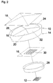
- the first imaging optical system 14 may be a lens system, in the entrance pupil a prism structure 18 in the form of a flat pyramid upstream. This is shown in FIG. 2.
- a prism structure 18 in the form of a flat pyramid upstream. This is shown in FIG. 2.
- a second imaging optical system 28 forms the intermediate image plane on the two-dimensional array 12 of detector elements.
- Micro-optical beam deflection element 30 contains two mutually displaceable Micro-optical lenticular grids 32 and 34 (Figure 3).
- the object-side micro-optical Linsertraster 32 formed by converging lenses 36.
- the image-side micro-optical Lens grid 34 is formed by diverging lenses 38.
- the lenticular grid 32 may be in Direction of arrow 40 are moved.
- the lenticular grid 34 may be in the direction of Arrow 42 are moved.
- the shift takes place in such a way that one after the other Rays from the different sectors 20, 22, 24 and 26 of the pupil of the first imaging optical system 14 to the second imaging optical system 28 passed and to form an image on the array 12 of detector elements be used.
- Detector elements sequentially detects the different sections of the field of view become. These sections are then stored in memory "electronically" to an overall picture composed of the field of view or the object scene. This can be a big one Field of view can be detected with the resolution of the arrangement 12 of Detector elements is delivered. This arrangement 12 would normally only one Capture smaller visual field.
- the displacement of the micro-optical lens grid 32 relative to the lenticular grid 34 to switch between the different sections of the field of view are small with respect to the grid dimension
- the lenticular grids 32 and 34 are in different Positions moves, whereby in each of these positions the rays from one of the Sectors 20, 22, 24 and 26 to the second optical system 28 directs.
- the different Positions are shown in Figures 6-9 and explained in more detail below.
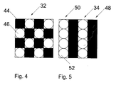
- FIG. 4 shows a detail of the micro-optical lenticular grid 32 in detail.
- the micro-optical lenticular grid 32 is checkerboard of opaque fields 44 and Micro-optical collecting lenses 46 constructed.
- Fig. 5 is a section of the other micro-optical lens grid 34 shown.
- the micro-optical lenticular grid 34 is off opaque strip 48 and in strips 50 of juxtaposed micro-optical Dispersing lenses 52 constructed.
- the lenticular screens are in different relative positions to each other shown.
- the detail 60 shown by a solid line in FIG corresponds to a plan view of the lenticular grids 32 and 34 in the position shown in Fig.3.
- Radiation, represented by an arrow 58 in Fig.3, through the converging lens 52 in occurs passes through the underlying in this position diverging lens 54 and falls on the detector element 56.
- the adjacent field 62 is opaque in the lenticular grid 32, so that no radiation is transmitted here.
- the adjacent fields 64 and 66 lie over the opaque strip 48 of the underlying lens grid 34. Through this Fields can therefore also no radiation
- Fig. 7 the situation is shown, in which the lenticular grid 32 by one field in Direction of arrow 40 has been moved. This movement takes place by means of piezo elements in only one direction. In this position, radiation will now pass through in field 62 Lenses while the field 52 is opaque.
- FIG 8 shows the situation in which not the lenticular grid 32, but the Lenticular grid 34 was moved relative to the position in Figure 6.
- the movement of the Lens grid 34 is in a direction indicated by an arrow 42 in FIG is. In this position, only radiation through the field 66 and the respectively passed through corresponding fields of each quadrant
- FIG. 9 shows the situation in which both lenticular grids 32 and 34 are in their position Movement direction by one field with respect to the situation shown in Figure 6 to be moved. In this case, the radiation through the field 64 through corresponding fields.
- Fig. 10 an arrangement is shown in which only an increase in resolution should be effected.
- the incident radiation 110 by means of a first imaged optical system 114 in an intermediate image plane 116 and with a detector 112 recorded.
- the prism structure 18 FIG. 2
- a Large pupil provided.
- the Switching of the optical microlens system in the intermediate image plane remains identical to the one described above.
Landscapes
- Engineering & Computer Science (AREA)
- Multimedia (AREA)
- Signal Processing (AREA)
- Transforming Light Signals Into Electric Signals (AREA)
Abstract
Description
- Fig. 1
- ist eine schematische Darstellung des optischen Aufbaus
- Fig.2
- ist eine schematisch-perspektivische Darstellung und veranschaulicht den Aufbau der optischen Systeme zur Erfassung verschiedener Blickfeklabschnitte bei der bildauflösenden Detektoranordnung von Fig. 1
- Fig.3
- ist eine perspektivische Darstellung von zwei mikrooptischen Linsenrastem und eines Detektorausschnitts
- Fig. 4
- zeigt den Aufbau eines ersten mikrooptischen Linsenrasters
- Fig.5
- zeigt den Aufbau eines zweiten inikrooptischen Linsenrasters
- Fig.6
- zeigt die mikrooptischen Linsenraster in einer ersten relativen Lage zueinander
- Fig.7
- zeigt die mikrooptischen Linsenraster in einer zweiten relativen Lage zueinander
- Fig.8
- zeigt die mikrooptischen Linsenraster in einer dritten relativen Lage zueinander
- Fig.9
- zeigt die mikrooptischen Linsenraster in einer vierten relativen Lage zueinander
- Fig. 10
- zeigt einen optischen Aufbau analog zu Fig.1 ohne Blickfeld-Erweiterung
Claims (6)
- Bildauflösende Detektoranordnung (10), auf welcher durch ein abbildendes optisches System (14) ein Bild einer Objektszene erzeugbar ist,(a) mit einer zweidimensionalen Anordnung (12) von Detektorelementen, wobei jedem Detektorelement in einer Bildebene ein Bildbereich zugeordnet ist und diese Bildbereiche ein Rastermaß definieren,(b) einem in dieser Bildebene (16) angeordneten Mikroblenden raster mit einem mit einem dem Rastermaß der Bddbereiche entsprechenden Rastermaß, wobei das Mikroblendenraster (32) ein Muster von durchlässigen und opaken Teilbereichen bildet,(c) das Mikroblendenraster in dieser Bildebene (16) schrittweise beweglich ist, derart daß in jeder Stellung nur Strahlung von einem einem Teilbereich jedes einem Detektorelement zugeordneten Bildbereichs auf das Detektorelement gelangt,
dadurch gekennzeichnet, daß(f) ein weiteres schrittweise bewegliches Mikroblendenraster (34) mit einem mit einem dem Rastemaß der Bildbereiche entsprechenden Rastermaß parallel zu dem ersten Mikroblendenraster (32) angeordnet ist, wobei das weitere Mikroblendenraster (32) ein weiteres Muster von durchlässigen und opaken Teilbereichen bildet,(g) beide Mikroblendenraster nur in jeweils einer Richtung (40; 42) senkrecht zur optischen Achse beweglich sind, wobei die Bewegungsrichtungen der beiden Mikroblendenraster einen von Null verschiedenen Winkel miteinander bilden und(h) durch Überlagerung der Muster der beiden Mikroblendenraster (32, 34) in jeder Stellung der Mikroblendenraster ein Muster gebildet wird das in jedem Bildbereich einen der betreffenden Stellung zugeordneten durchlässigen Teilbereich aufweist. - Detektoranordnung nach Anpruch 1, dadurch gekennzeichnet, daß die Mikroblendenraster (32, 34) senkrecht zueinander beweglich sind.
- Detektoranordnung nach Anspruch 2, dadurch gekennzeichnet, daß das erste Mikroblendenraster (32) schachbrettartig aus Feldern (44, 46) zum abwechselnden Blockieren und Durchlässen der Strahlung aufgebaut ist und das andere Mikroblendenraster (34) die Strahlung entlang von Streifen (48) blockiert, welche die gleiche Breite wie ein Feld des erstem Mikroblendenrasters (32) haben, und sich die Bewegungsrichtung senkrecht zu diesen Streifen erstreckt.
- Detektoranordnung nach einem der vorgehenden Ansprüche, dadurch gekennzeichnet, daß wenigstens eines der Mikroblendenraster (32, 34) als Mikro-Linsen-Blendenarray ausgebildet ist.
- Detektoranordnung nach Anspruch 4. dadurch gekennzeichnet, daß das dem Detektor abgewandte Mikro-Linsen-Blendenarray (32) als Mikro-Sammellinsen-Blendenarray ausgebildet ist und das detektorseitige Mikro-Linsen-Blendenarrav (34) als Mikro-Streulinsen-Array ausgebildet ist.
- Detektoranordnung nach Anspruch 5, dadurch gekennzeichnet, daß ein erstes abbildendes optisches System (14) vorgesehen, ist, in dessen Pupille eine Mehrzahi von Pupillen-Bereichen gebildet sind, von denen jeder ein Gesichtsfeld auf einen gemeinsamen Bildebenen-Bereich abbildet, in welchem die Mikro-Blenden-Arrays angeordnet sind.
Applications Claiming Priority (2)
| Application Number | Priority Date | Filing Date | Title |
|---|---|---|---|
| DE10225340 | 2002-06-06 | ||
| DE10225340 | 2002-06-06 |
Publications (3)
| Publication Number | Publication Date |
|---|---|
| EP1370073A2 true EP1370073A2 (de) | 2003-12-10 |
| EP1370073A3 EP1370073A3 (de) | 2006-04-19 |
| EP1370073B1 EP1370073B1 (de) | 2010-10-06 |
Family
ID=29432695
Family Applications (1)
| Application Number | Title | Priority Date | Filing Date |
|---|---|---|---|
| EP03005889A Expired - Lifetime EP1370073B1 (de) | 2002-06-06 | 2003-03-17 | Bildauflösende Detektoranordnung |
Country Status (2)
| Country | Link |
|---|---|
| EP (1) | EP1370073B1 (de) |
| DE (1) | DE50313149D1 (de) |
Cited By (1)
| Publication number | Priority date | Publication date | Assignee | Title |
|---|---|---|---|---|
| DE102010006662A1 (de) * | 2010-02-03 | 2011-08-04 | Diehl BGT Defence GmbH & Co. KG, 88662 | Vorrichtung und Verfahren zum Abbilden einer Umgebung auf eine Detektoreinrichtung |
Family Cites Families (2)
| Publication number | Priority date | Publication date | Assignee | Title |
|---|---|---|---|---|
| US5059008A (en) * | 1990-03-26 | 1991-10-22 | General Electric Company | Wide angle beam steerer using translation of plural lens arrays |
| DE19904914A1 (de) * | 1999-02-06 | 2000-08-10 | Bodenseewerk Geraetetech | Bildauflösende Detektoranordnung |
-
2003
- 2003-03-17 DE DE50313149T patent/DE50313149D1/de not_active Expired - Lifetime
- 2003-03-17 EP EP03005889A patent/EP1370073B1/de not_active Expired - Lifetime
Cited By (2)
| Publication number | Priority date | Publication date | Assignee | Title |
|---|---|---|---|---|
| DE102010006662A1 (de) * | 2010-02-03 | 2011-08-04 | Diehl BGT Defence GmbH & Co. KG, 88662 | Vorrichtung und Verfahren zum Abbilden einer Umgebung auf eine Detektoreinrichtung |
| DE102010006662B4 (de) | 2010-02-03 | 2019-07-25 | Diehl Defence Gmbh & Co. Kg | Vorrichtung und Verfahren zum Abbilden einer Umgebung auf eine Detektoreinrichtung |
Also Published As
| Publication number | Publication date |
|---|---|
| EP1370073B1 (de) | 2010-10-06 |
| EP1370073A3 (de) | 2006-04-19 |
| DE50313149D1 (de) | 2010-11-18 |
Similar Documents
| Publication | Publication Date | Title |
|---|---|---|
| EP3167605A1 (de) | Vorrichtung und verfahren zur erfassung eines objektbereichs | |
| DE102014214750B3 (de) | Bildaufnahmesystem mit schnell vibrierendem Global-Shutter-CMOS-Sensor | |
| EP0449859B1 (de) | Verfahren und vorrichtung zur beobachtung von moiremustern von zu untersuchenden oberflächen unter anwendung des moireverfahrens mit phasenshiften | |
| WO2014086511A1 (de) | Inspektionsvorrichtung | |
| DE3340647A1 (de) | Verfahren zur fokussierung eines mikroskopes sowie mikroskop zur durchfuehrung des verfahrens | |
| DE69117737T2 (de) | Spectrumsabhängiger dither und farbfiltermaske zur erhöhung der blauempfindlichkeit des bildsensors | |
| DE69718009T2 (de) | System zur optischen detektion | |
| EP0916971B1 (de) | Schaltbares, mikrooptisches Strahlenumlenksystem | |
| EP1370073B1 (de) | Bildauflösende Detektoranordnung | |
| DE102006058057B3 (de) | Verfahren und Vorrichtung zur optischen Erfassung einer Struktur | |
| EP1026879A2 (de) | Bildauflösende Detektoranordnung | |
| DE2838121C3 (de) | ||
| DE3111300C2 (de) | ||
| EP1377037B1 (de) | Optisches System mit umschaltbaren Gesichtsfeldern | |
| DE69321090T2 (de) | Verfahren und Vorrichtung zur Analyse von sich bewegenden Objekten mittels Radiographie | |
| DE102005036770B4 (de) | Kamera | |
| EP1389737B1 (de) | Weitwinkelsucher mit schaltbarem Mikroblendenraster | |
| WO2001098816A1 (de) | Verfahren und anordnung zur aufnahme von mehreren ansichten einer szene oder eines gegenstandes | |
| DE102013200059B4 (de) | Vorrichtung zur Aufnahme eines von einer Hauptlinse einer plenoptischen Kamera erzeugten Zwischenbilds und plenoptische Kamera | |
| DE102004018182B4 (de) | Vorrichtung und Verfahren zur Erzeugung einer Abbildung einer Objektszene | |
| DE19502860C1 (de) | Röntgendiagnostikeinrichtung | |
| EP4351159B1 (de) | Bildsensor | |
| DE102021202164B3 (de) | Tandemblendenarchitektur zur Füllfaktorerhöhung von kompakten Multikanalabbildungssystemen | |
| EP2187617A1 (de) | Anordnung zur flugkörpergestützten Bilddatenaufnahme von der Oberfläche eines Himmelskörpers | |
| DE4200961A1 (de) | Verfahren und vorrichtung zur realisierung hochaufloesender kamerasysteme |
Legal Events
| Date | Code | Title | Description |
|---|---|---|---|
| PUAI | Public reference made under article 153(3) epc to a published international application that has entered the european phase |
Free format text: ORIGINAL CODE: 0009012 |
|
| AK | Designated contracting states |
Kind code of ref document: A2 Designated state(s): AT BE BG CH CY CZ DE DK EE ES FI FR GB GR HU IE IT LI LU MC NL PT RO SE SI SK TR |
|
| AX | Request for extension of the european patent |
Extension state: AL LT LV MK RO |
|
| RAP1 | Party data changed (applicant data changed or rights of an application transferred) |
Owner name: DIEHL BGT DEFENCE GMBH & CO.KG |
|
| PUAL | Search report despatched |
Free format text: ORIGINAL CODE: 0009013 |
|
| AK | Designated contracting states |
Kind code of ref document: A3 Designated state(s): AT BE BG CH CY CZ DE DK EE ES FI FR GB GR HU IE IT LI LU MC NL PT RO SE SI SK TR |
|
| AX | Request for extension of the european patent |
Extension state: AL LT LV MK RO |
|
| 17P | Request for examination filed |
Effective date: 20060518 |
|
| AKX | Designation fees paid |
Designated state(s): DE FR GB SE |
|
| 17Q | First examination report despatched |
Effective date: 20061221 |
|
| GRAP | Despatch of communication of intention to grant a patent |
Free format text: ORIGINAL CODE: EPIDOSNIGR1 |
|
| GRAS | Grant fee paid |
Free format text: ORIGINAL CODE: EPIDOSNIGR3 |
|
| GRAA | (expected) grant |
Free format text: ORIGINAL CODE: 0009210 |
|
| AK | Designated contracting states |
Kind code of ref document: B1 Designated state(s): DE FR GB SE |
|
| REG | Reference to a national code |
Ref country code: GB Ref legal event code: FG4D Free format text: NOT ENGLISH |
|
| REF | Corresponds to: |
Ref document number: 50313149 Country of ref document: DE Date of ref document: 20101118 Kind code of ref document: P |
|
| REG | Reference to a national code |
Ref country code: SE Ref legal event code: TRGR |
|
| PGFP | Annual fee paid to national office [announced via postgrant information from national office to epo] |
Ref country code: SE Payment date: 20110314 Year of fee payment: 9 |
|
| PLBE | No opposition filed within time limit |
Free format text: ORIGINAL CODE: 0009261 |
|
| STAA | Information on the status of an ep patent application or granted ep patent |
Free format text: STATUS: NO OPPOSITION FILED WITHIN TIME LIMIT |
|
| 26N | No opposition filed |
Effective date: 20110707 |
|
| REG | Reference to a national code |
Ref country code: DE Ref legal event code: R097 Ref document number: 50313149 Country of ref document: DE Effective date: 20110707 |
|
| PGFP | Annual fee paid to national office [announced via postgrant information from national office to epo] |
Ref country code: FR Payment date: 20120403 Year of fee payment: 10 |
|
| PGFP | Annual fee paid to national office [announced via postgrant information from national office to epo] |
Ref country code: GB Payment date: 20120322 Year of fee payment: 10 |
|
| PGFP | Annual fee paid to national office [announced via postgrant information from national office to epo] |
Ref country code: DE Payment date: 20120509 Year of fee payment: 10 |
|
| REG | Reference to a national code |
Ref country code: SE Ref legal event code: EUG |
|
| PG25 | Lapsed in a contracting state [announced via postgrant information from national office to epo] |
Ref country code: SE Free format text: LAPSE BECAUSE OF NON-PAYMENT OF DUE FEES Effective date: 20120318 |
|
| GBPC | Gb: european patent ceased through non-payment of renewal fee |
Effective date: 20130317 |
|
| REG | Reference to a national code |
Ref country code: FR Ref legal event code: ST Effective date: 20131129 |
|
| REG | Reference to a national code |
Ref country code: DE Ref legal event code: R119 Ref document number: 50313149 Country of ref document: DE Effective date: 20131001 |
|
| PG25 | Lapsed in a contracting state [announced via postgrant information from national office to epo] |
Ref country code: GB Free format text: LAPSE BECAUSE OF NON-PAYMENT OF DUE FEES Effective date: 20130317 Ref country code: FR Free format text: LAPSE BECAUSE OF NON-PAYMENT OF DUE FEES Effective date: 20130402 Ref country code: DE Free format text: LAPSE BECAUSE OF NON-PAYMENT OF DUE FEES Effective date: 20131001 |