EP1369786A2 - Method and apparatus for providing fault-tolerance for temporary results within a central processing unit - Google Patents
Method and apparatus for providing fault-tolerance for temporary results within a central processing unit Download PDFInfo
- Publication number
- EP1369786A2 EP1369786A2 EP03252741A EP03252741A EP1369786A2 EP 1369786 A2 EP1369786 A2 EP 1369786A2 EP 03252741 A EP03252741 A EP 03252741A EP 03252741 A EP03252741 A EP 03252741A EP 1369786 A2 EP1369786 A2 EP 1369786A2
- Authority
- EP
- European Patent Office
- Prior art keywords
- temporary
- cpu
- temporary result
- result
- annex
- Prior art date
- Legal status (The legal status is an assumption and is not a legal conclusion. Google has not performed a legal analysis and makes no representation as to the accuracy of the status listed.)
- Granted
Links
Images


Classifications
-
- G—PHYSICS
- G06—COMPUTING OR CALCULATING; COUNTING
- G06F—ELECTRIC DIGITAL DATA PROCESSING
- G06F11/00—Error detection; Error correction; Monitoring
- G06F11/07—Responding to the occurrence of a fault, e.g. fault tolerance
- G06F11/08—Error detection or correction by redundancy in data representation, e.g. by using checking codes
- G06F11/10—Adding special bits or symbols to the coded information, e.g. parity check, casting out 9's or 11's
- G06F11/1008—Adding special bits or symbols to the coded information, e.g. parity check, casting out 9's or 11's in individual solid state devices
- G06F11/1012—Adding special bits or symbols to the coded information, e.g. parity check, casting out 9's or 11's in individual solid state devices using codes or arrangements adapted for a specific type of error
- G06F11/1032—Simple parity
-
- G—PHYSICS
- G06—COMPUTING OR CALCULATING; COUNTING
- G06F—ELECTRIC DIGITAL DATA PROCESSING
- G06F11/00—Error detection; Error correction; Monitoring
- G06F11/07—Responding to the occurrence of a fault, e.g. fault tolerance
- G06F11/14—Error detection or correction of the data by redundancy in operations
- G06F11/1402—Saving, restoring, recovering or retrying
- G06F11/1405—Saving, restoring, recovering or retrying at machine instruction level
-
- G—PHYSICS
- G06—COMPUTING OR CALCULATING; COUNTING
- G06F—ELECTRIC DIGITAL DATA PROCESSING
- G06F9/00—Arrangements for program control, e.g. control units
- G06F9/06—Arrangements for program control, e.g. control units using stored programs, i.e. using an internal store of processing equipment to receive or retain programs
- G06F9/30—Arrangements for executing machine instructions, e.g. instruction decode
- G06F9/38—Concurrent instruction execution, e.g. pipeline or look ahead
- G06F9/3836—Instruction issuing, e.g. dynamic instruction scheduling or out of order instruction execution
-
- G—PHYSICS
- G06—COMPUTING OR CALCULATING; COUNTING
- G06F—ELECTRIC DIGITAL DATA PROCESSING
- G06F9/00—Arrangements for program control, e.g. control units
- G06F9/06—Arrangements for program control, e.g. control units using stored programs, i.e. using an internal store of processing equipment to receive or retain programs
- G06F9/30—Arrangements for executing machine instructions, e.g. instruction decode
- G06F9/38—Concurrent instruction execution, e.g. pipeline or look ahead
- G06F9/3854—Instruction completion, e.g. retiring, committing or graduating
- G06F9/3858—Result writeback, i.e. updating the architectural state or memory
-
- G—PHYSICS
- G06—COMPUTING OR CALCULATING; COUNTING
- G06F—ELECTRIC DIGITAL DATA PROCESSING
- G06F9/00—Arrangements for program control, e.g. control units
- G06F9/06—Arrangements for program control, e.g. control units using stored programs, i.e. using an internal store of processing equipment to receive or retain programs
- G06F9/30—Arrangements for executing machine instructions, e.g. instruction decode
- G06F9/38—Concurrent instruction execution, e.g. pipeline or look ahead
- G06F9/3861—Recovery, e.g. branch miss-prediction, exception handling
Definitions
- the present invention relates to providing fault-tolerance within computer systems, including fault-tolerance for temporary results within a central processing unit (CPU) before the temporary results are committed to the architectural state of the CPU.
- CPU central processing unit
- microprocessor systems use error-correcting codes to protect data stored in cache memories within a microprocessor chip.
- cache memory accounts for a considerable portion of the memory within a microprocessor chip, many other memory elements remain unprotected.
- an annex also called a result buffer or working register file
- an annex can include hundreds of registers, which makes it likely that a random bit error will eventually occur within the annex.
- An annex stores temporary results of computational operations that are waiting to be committed to the architectural state of the central processing unit (CPU). For example, the annex may store the result of an addition operation before the result is ready to be written to a destination register in the CPU. When the result is ultimately written to the destination register, which is located in a register file defined by the instruction set architecture, it becomes "architecturally visible".
- One embodiment of the present invention provides a system that corrects bit errors in temporary results within a central processing unit (CPU).
- the system receives a temporary result during execution of an in-flight instruction.
- the system generates a parity bit for the temporary result, and stores the temporary result and the parity bit in a temporary register within the CPU.
- the system checks the temporary result and the parity bit to detect a bit error. If a bit error is detected, the system performs a micro-trap operation to re-execute the instruction that generated the temporary result, thereby regenerating the temporary result. Otherwise, if a bit error is not detected, the system commits the temporary result to the architectural state of the CPU.
- Such an approach helps to provide a method and an apparatus for fixing random bit errors that occur in temporary results, without the above-described problems of using error-correcting codes.
- the temporary register is located within an annex that stores temporary results for in-flight instructions before the temporary results are written to a register file.
- the annex can be a result buffer that temporarily holds results produced out-of-order until they can be retired in-order.
- the annex is organized as a first-in-first-out (FIFO) structure with pipeline stages through which the temporary result and the parity bit advance.
- FIFO first-in-first-out
- the system allows younger instructions to lookup temporary results in the annex, instead of having to wait for the temporary results to be committed to the register file.
- This lookup process can involve performing a content addressable memory (CAM) search for a specific destination register index. Note that because it is possible for a given destination register to appear more than once in the annex, the CAM search can possibly return more than one temporary result. In order to handle this possibility, the CAM search can be performed using a "priority CAM", which returns the matching temporary result generated by the latest instruction in the execution ordering specified by the program.
- CAM content addressable memory
- committing the temporary result to the architectural state of the CPU involves writing the temporary result to an architecturally visible register within a register file.
- the micro-trap operation flushes the instruction pipeline of the CPU.
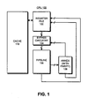
- FIG. 1 illustrates the structure of a central processing unit (CPU) 100 in accordance with one embodiment of the present invention.
- CPU 100 can generally reside within any type of computer system, including, but not limited to, a computer system based on a microprocessor, a mainframe computer, a digital signal processor, a portable computing device, a personal organizer, a device controller, and a computational engine within an appliance.
- CPU 100 includes a register file 102 for storing operands for computational operations and results of computational operations.
- CPU 100 also includes a cache 110 for storing code and data.
- cache 110 can include a separate instruction cache and data cache.
- cache 110 can be a level-one (L1) cache that communicates with one or more lower-level caches.
- operands from register file 102 pass through pipeline 106, which performs computational operations on the operands to produce one or more results. These results are written back to register file 102.
- Pipeline 106 feeds temporary results into an annex 108, which stores the temporary results until they are ready to be committed to register file 102.
- Bypass circuitry 104 allows pipeline 106 to receive operands from either register file 102 or annex 108. This allows a temporary result to feed back directly into pipeline 106, without having to first be written into register file 102.
- bypass circuitry 104 causes the temporary result to feed into pipeline 106 in place of the stale value retrieved from register file 102.
- FIG. 2 illustrates the structure of annex 108 in accordance with one embodiment of the present invention. As is illustrated in FIG. 2, annex 108 receives temporary results from pipeline 106.
- Pipeline 106 can contain various computational circuitry.
- pipeline 106 includes a floating-point adder circuit 202, which is made up of a number of pipeline stages 243-246.
- Pipeline 106 also includes integer arithmetic logic unit (ALU) 207 and integer ALU 208. Note that ALU 207 and ALU 208 produce temporary results that wait in annex 108 until floating-point adder circuit 202 generates a related result. This allows the temporary results and the related result to be simultaneously committed to register file 102.
- ALU integer arithmetic logic unit
- ALU 207 receives operands from multiplexers 203 and 204 within bypass circuitry 104. Multiplexers 203 and 204 allow ALU 207 to receive operands from either register file 102 or annex 108. Similarly, ALU 208 receives operands from multiplexers 203 and 204 within bypass circuitry 104, and this allows ALU 208 to receive operations from either register file 102 or annex 108. Note that in some embodiments, the inputs to floating point adder circuit 202 may also be received from annex 108.
- the output of ALU 207 is latched into dataword register 209.
- the output of dataword register 209 passes through parity generation circuit 211 to generate a parity bit 213.
- This parity bit 213 moves along with its associated dataword 214 and an associated register destination index 215 through a number of pipeline stages in annex 108.
- parity bit 225 and dataword 226 pass through parity checking circuit 237, which generates an error signal 241.
- Error signal 241 indicates if there is a parity error in the combination of parity bit 225 and dataword 226. If so, the system performs a micro-trap instruction to correct the error as is described in more detail below with reference to FIG. 3.
- register destination indices 215, 221, 227 and 233 feed into content-addressable memory (CAM) circuit 139, which performs a CAM search to determine if the index of a target register (currently being retrieved from register file 102) matches one or more of register destination indices 215, 221, 227 and 233. If there is a match, the target register contains stale data. In this case, CAM circuit 139 forwards the most current temporary value, generated by the latest instruction in the execution ordering specified by the program, to bypass circuitry 104. This allows bypass circuitry 104 to forward the most current temporary value to pipeline 106 instead of the stale value retrieved from register file 102.
- CAM content-addressable memory
- ALU 208 passes through a similar set of pipeline stages within annex 108.
- FIG. 3 is a flow chart illustrating the process of providing error correction for a temporary result in accordance with one embodiment of the present invention.
- ALU 207 produces a temporary result for an in-flight transaction, which is stored in dataword register 209 (step 302) (see FIG. 2).
- the system uses parity generation circuit 211 to generate a parity bit 213 from the temporary result (step 304).
- the system then passes the temporary result, the parity bit and an associated register destination index through pipeline stages within annex 108. While in transit through annex 108, a younger instruction is allowed to read the temporary result to perform a bypass operation if the younger instruction is retrieving an operand from a register that matches the associated register destination (step 306).
- the system uses parity checking circuit 237 to check the parity of the dataword and associated parity bit (step 308).
- the system performs a micro-trap operation, which flushes the pipeline and restarts execution from the instruction that generated the corrupted temporary result (step 312). This causes the instruction to be executed again, which regenerates the temporary result.
- the present invention can be applied to any temporary result that is generated by a CPU, and is not meant to be limited to the specific temporary results located within annex 108 , such as illustrated in FIG. 2.
- the temporary results may be stored in registers that are not architecturally visible within register file 102. These non-visible registers are sometimes referred to as a "working register file” for storing temporary results, as opposed to an "architectural register file” for storing results that are architecturally visible. Accordingly, many modifications and variations will be apparent to practitioners skilled in the art, and so the scope of the present invention is to be defined by the appended claims.
Landscapes
- Engineering & Computer Science (AREA)
- Theoretical Computer Science (AREA)
- Software Systems (AREA)
- Physics & Mathematics (AREA)
- General Engineering & Computer Science (AREA)
- General Physics & Mathematics (AREA)
- Quality & Reliability (AREA)
- Advance Control (AREA)
- Retry When Errors Occur (AREA)
Abstract
Description
Claims (20)
- A method for providing fault-tolerance for temporary results within a central processing unit (CPU), comprising:receiving a temporary result for an in-flight instruction;generating a parity bit for the temporary result;storing the temporary result and the parity bit in a temporary register within the CPU;before the temporary result is committed to the architectural state of the CPU, checking the temporary result and the parity bit to detect a bit error;if a bit error is detected, performing a micro-trap operation to re-execute the instruction that generated the temporary result, thereby regenerating the temporary result; andif a bit error is not detected, committing the temporary result to the architectural state of the CPU.
- The method of claim 1, wherein the temporary register is located within an annex that stores temporary results for in-flight instructions before the temporary results are written to a register file.
- The method of claim 2,
wherein the annex is organized as a first-in-first-out (FIFO) structure with pipeline stages; and
wherein the temporary result and the parity bit advance through the pipeline stages. - The method of claim 2 or 3, further comprising allowing younger instructions to read temporary results from the annex instead of having to wait for the temporary results to be committed to the register file.
- The method of claim 4, wherein reading a specific temporary result from the annex involves performing a content addressable memory (CAM) search for a specific destination register index that is associated with the specific temporary result.
- The method of any preceding claim , wherein committing the temporary result to the architectural state of the CPU involves writing the temporary result to an architecturally visible register within a register file.
- The method of any preceding claim, wherein performing the micro-trap operation involves flushing the instruction pipeline of the CPU.
- An apparatus that provides fault-tolerance for temporary results within a central processing unit (CPU), comprising:the CPU;a parity generation circuit with the CPU that is configured to generate a parity bit for a temporary result that is associated with an in-flight instruction;at least one temporary register within the CPU for storing the temporary result and the parity bit;a parity checking circuit that is configured to check the temporary result and the parity bit to detect a bit error before the temporary result is committed to the architectural state of the CPU; anda micro-trap mechanism, wherein if a bit error is detected, the micro-trap mechanism is configured to perform a micro-trap operation to re-execute the instruction that generated the temporary result, thereby regenerating the temporary result.
- The apparatus of claim 8, further comprising a writing mechanism, wherein if a bit error is not detected, the writing mechanism is configured to commit the temporary result to the architectural state of the CPU.
- The apparatus of claim 9, wherein the writing mechanism is configured to write the temporary result to an architecturally visible register within a register file.
- The apparatus of any of claims 8 to 10, wherein the temporary register is located within an annex that stores temporary results for in-flight instructions before the temporary results are written to a register file.
- The apparatus of claim 11,
wherein the annex is organized as a first-in-first-out (FIFO) structure with pipeline stages; and
wherein the annex is configured so that the temporary result and the parity bit advance through the pipeline stages. - The apparatus of claim 11 or 12, wherein the annex is configured to allow younger instructions to read temporary results from the annex instead of having to wait for the temporary results to be committed to the register file.
- The apparatus of any of claims 8 to 13, wherein the annex is configured to support a content addressable memory (CAM) search for a temporary result associated with a specific destination register index.
- The apparatus of any of claims 8 to 14, wherein the micro-trap mechanism is configure to flush the instruction pipeline of the CPU.
- An apparatus that provides fault-tolerance for temporary results comprising:wherein the temporary register is located within an annex that stores temporary results for in-flight instructions;a CPU;a register file within the CPU;a parity generation circuit with the CPU that is configured to generate a parity bit for a temporary result that is associated with an in-flight instruction;a temporary register within the CPU for storing the temporary result and the parity bit;
wherein the annex is configured to allowing younger instructions to read temporary results from the annex instead of having to wait for the temporary results to be committed to the register file;
a parity checking circuit within the CPU that is configured to check the temporary result and the parity bit to detect a bit error before the temporary result is written to the register file; and
a micro-trap mechanism, wherein if a bit error is detected, the micro-trap mechanism is configured to perform a micro-trap operation to re-execute the instruction that generated the temporary result, thereby regenerating the temporary result. - The apparatus of claim 16,
wherein the annex is organized as a first-in-first-out (FIFO) structure with pipeline stages; and
wherein the annex is configured so that the temporary result and the parity bit advance through the pipeline stages. - The apparatus of claim 16 or 17, wherein the annex is configured to support a content addressable memory (CAM) search for a temporary result associated with a specific destination register index.
- The apparatus of any of claims 16 to 18, wherein the micro-trap mechanism is configure to flush the instruction pipeline of the CPU.
- A computer system that provides fault-tolerance for temporary results comprising:a CPU;a main memory;a secondary storage device;a parity generation circuit with the CPU that is configured to generate a parity bit for a temporary result that is associated with an in-flight instruction;at least one temporary register within the CPU for storing the temporary result and the parity bit;a parity checking circuit within the CPU that is configured to check the temporary result and the parity bit to detect a bit error before the temporary result is committed to the architectural state of the CPU; anda micro-trap mechanism, wherein if a bit error is detected, the micro-trap mechanism is configured to perform a micro-trap operation to re-execute the instruction that generated the temporary result, thereby regenerating the temporary result.
Applications Claiming Priority (2)
| Application Number | Priority Date | Filing Date | Title |
|---|---|---|---|
| US146102 | 2002-05-14 | ||
| US10/146,102 US7124331B2 (en) | 2002-05-14 | 2002-05-14 | Method and apparatus for providing fault-tolerance for temporary results within a CPU |
Publications (3)
| Publication Number | Publication Date |
|---|---|
| EP1369786A2 true EP1369786A2 (en) | 2003-12-10 |
| EP1369786A3 EP1369786A3 (en) | 2005-03-23 |
| EP1369786B1 EP1369786B1 (en) | 2006-12-13 |
Family
ID=29548277
Family Applications (1)
| Application Number | Title | Priority Date | Filing Date |
|---|---|---|---|
| EP03252741A Expired - Lifetime EP1369786B1 (en) | 2002-05-14 | 2003-04-30 | Method and apparatus for providing fault-tolerance for temporary results within a central processing unit |
Country Status (3)
| Country | Link |
|---|---|
| US (1) | US7124331B2 (en) |
| EP (1) | EP1369786B1 (en) |
| DE (1) | DE60310308T2 (en) |
Cited By (1)
| Publication number | Priority date | Publication date | Assignee | Title |
|---|---|---|---|---|
| EP1851639A4 (en) * | 2005-02-15 | 2010-09-01 | Maxwell Technologies Inc | System and method for effectively implementing an immunity mode in an electronic device |
Families Citing this family (4)
| Publication number | Priority date | Publication date | Assignee | Title |
|---|---|---|---|---|
| US7383464B2 (en) * | 2003-12-08 | 2008-06-03 | International Business Machines Corporation | Non-inline transaction error correction |
| US9529671B2 (en) | 2014-06-17 | 2016-12-27 | Arm Limited | Error detection in stored data values |
| US9760438B2 (en) * | 2014-06-17 | 2017-09-12 | Arm Limited | Error detection in stored data values |
| US9891976B2 (en) | 2015-02-26 | 2018-02-13 | Arm Limited | Error detection circuitry for use with memory |
Family Cites Families (10)
| Publication number | Priority date | Publication date | Assignee | Title |
|---|---|---|---|---|
| EP0077153B1 (en) * | 1981-10-01 | 1987-03-04 | Stratus Computer, Inc. | Digital data processor with fault-tolerant bus protocol |
| BR8503913A (en) * | 1984-08-18 | 1986-05-27 | Fujitsu Ltd | ERROR RECOVERY SYSTEM AND PROCESS IN A CHANNEL DATA PROCESSOR HAVING A CONTROL MEMORY DEVICE AND ERROR RECOVERY PROCESS IN A CHANNEL TYPE DATA PROCESSOR |
| JPS6226580A (en) * | 1985-07-29 | 1987-02-04 | Hitachi Ltd | Trouble processing system |
| US5150469A (en) * | 1988-12-12 | 1992-09-22 | Digital Equipment Corporation | System and method for processor pipeline control by selective signal deassertion |
| US5487156A (en) * | 1989-12-15 | 1996-01-23 | Popescu; Valeri | Processor architecture having independently fetching issuing and updating operations of instructions which are sequentially assigned and stored in order fetched |
| US5276862A (en) * | 1991-04-09 | 1994-01-04 | Bull Hn Information Systems Inc. | Safestore frame implementation in a central processor |
| US6226338B1 (en) * | 1998-06-18 | 2001-05-01 | Lsi Logic Corporation | Multiple channel data communication buffer with single transmit and receive memories |
| US6122656A (en) * | 1998-07-31 | 2000-09-19 | Advanced Micro Devices, Inc. | Processor configured to map logical register numbers to physical register numbers using virtual register numbers |
| US6163837A (en) * | 1998-11-17 | 2000-12-19 | Sun Microsystems, Inc. | Writing of instruction results produced by instruction execution circuits to result destinations |
| US6542988B1 (en) | 1999-10-01 | 2003-04-01 | Sun Microsystems, Inc. | Sending both a load instruction and retrieved data from a load buffer to an annex prior to forwarding the load data to register file |
-
2002
- 2002-05-14 US US10/146,102 patent/US7124331B2/en not_active Expired - Lifetime
-
2003
- 2003-04-30 EP EP03252741A patent/EP1369786B1/en not_active Expired - Lifetime
- 2003-04-30 DE DE60310308T patent/DE60310308T2/en not_active Expired - Lifetime
Cited By (1)
| Publication number | Priority date | Publication date | Assignee | Title |
|---|---|---|---|---|
| EP1851639A4 (en) * | 2005-02-15 | 2010-09-01 | Maxwell Technologies Inc | System and method for effectively implementing an immunity mode in an electronic device |
Also Published As
| Publication number | Publication date |
|---|---|
| US20040078728A1 (en) | 2004-04-22 |
| US7124331B2 (en) | 2006-10-17 |
| DE60310308T2 (en) | 2007-06-21 |
| EP1369786B1 (en) | 2006-12-13 |
| DE60310308D1 (en) | 2007-01-25 |
| EP1369786A3 (en) | 2005-03-23 |
Similar Documents
| Publication | Publication Date | Title |
|---|---|---|
| US7478276B2 (en) | Method for checkpointing instruction groups with out-of-order floating point instructions in a multi-threaded processor | |
| US7865769B2 (en) | In situ register state error recovery and restart mechanism | |
| US5887161A (en) | Issuing instructions in a processor supporting out-of-order execution | |
| US7921331B2 (en) | Write filter cache method and apparatus for protecting the microprocessor core from soft errors | |
| US8627044B2 (en) | Issuing instructions with unresolved data dependencies | |
| US7133969B2 (en) | System and method for handling exceptional instructions in a trace cache based processor | |
| US6941489B2 (en) | Checkpointing of register file | |
| US6973563B1 (en) | Microprocessor including return prediction unit configured to determine whether a stored return address corresponds to more than one call instruction | |
| US5913048A (en) | Dispatching instructions in a processor supporting out-of-order execution | |
| US6098167A (en) | Apparatus and method for fast unified interrupt recovery and branch recovery in processors supporting out-of-order execution | |
| US7409589B2 (en) | Method and apparatus for reducing number of cycles required to checkpoint instructions in a multi-threaded processor | |
| US7590826B2 (en) | Speculative data value usage | |
| US9875105B2 (en) | Checkpointed buffer for re-entry from runahead | |
| US20020073357A1 (en) | Multiprocessor with pair-wise high reliability mode, and method therefore | |
| US6543028B1 (en) | Silent data corruption prevention due to instruction corruption by soft errors | |
| US20100131796A1 (en) | System and Method for Detecting and Recovering from Errors in an Instruction Stream of an Electronic Data Processing System | |
| US20110238962A1 (en) | Register Checkpointing for Speculative Modes of Execution in Out-of-Order Processors | |
| JP3183837B2 (en) | How to detect load queue and bypass errors | |
| JP3577052B2 (en) | Instruction issuing device and instruction issuing method | |
| US11740973B2 (en) | Instruction error handling | |
| US7058877B2 (en) | Method and apparatus for providing error correction within a register file of a CPU | |
| US20050081195A1 (en) | Selectively deferring the execution of instructions with unresolved data dependencies as they are issued in program order | |
| US6507928B1 (en) | Processor cache system with parity protection and method of operation | |
| US7124331B2 (en) | Method and apparatus for providing fault-tolerance for temporary results within a CPU | |
| US20160065243A1 (en) | Radiation hardening architectural extensions for a radiation hardened by design microprocessor |
Legal Events
| Date | Code | Title | Description |
|---|---|---|---|
| PUAI | Public reference made under article 153(3) epc to a published international application that has entered the european phase |
Free format text: ORIGINAL CODE: 0009012 |
|
| AK | Designated contracting states |
Kind code of ref document: A2 Designated state(s): AT BE BG CH CY CZ DE DK EE ES FI FR GB GR HU IE IT LI LU MC NL PT RO SE SI SK TR |
|
| AX | Request for extension of the european patent |
Extension state: AL LT LV MK |
|
| PUAL | Search report despatched |
Free format text: ORIGINAL CODE: 0009013 |
|
| AK | Designated contracting states |
Kind code of ref document: A3 Designated state(s): AT BE BG CH CY CZ DE DK EE ES FI FR GB GR HU IE IT LI LU MC NL PT RO SE SI SK TR |
|
| AX | Request for extension of the european patent |
Extension state: AL LT LV MK |
|
| RIC1 | Information provided on ipc code assigned before grant |
Ipc: 7G 06F 9/38 B Ipc: 7G 06F 11/10 A Ipc: 7G 06F 11/14 B |
|
| 17P | Request for examination filed |
Effective date: 20050914 |
|
| AKX | Designation fees paid |
Designated state(s): DE FR GB |
|
| GRAP | Despatch of communication of intention to grant a patent |
Free format text: ORIGINAL CODE: EPIDOSNIGR1 |
|
| GRAS | Grant fee paid |
Free format text: ORIGINAL CODE: EPIDOSNIGR3 |
|
| GRAA | (expected) grant |
Free format text: ORIGINAL CODE: 0009210 |
|
| AK | Designated contracting states |
Kind code of ref document: B1 Designated state(s): DE FR GB |
|
| REG | Reference to a national code |
Ref country code: GB Ref legal event code: FG4D |
|
| REF | Corresponds to: |
Ref document number: 60310308 Country of ref document: DE Date of ref document: 20070125 Kind code of ref document: P |
|
| EN | Fr: translation not filed | ||
| PLBE | No opposition filed within time limit |
Free format text: ORIGINAL CODE: 0009261 |
|
| STAA | Information on the status of an ep patent application or granted ep patent |
Free format text: STATUS: NO OPPOSITION FILED WITHIN TIME LIMIT |
|
| 26N | No opposition filed |
Effective date: 20070914 |
|
| PG25 | Lapsed in a contracting state [announced via postgrant information from national office to epo] |
Ref country code: FR Free format text: LAPSE BECAUSE OF FAILURE TO SUBMIT A TRANSLATION OF THE DESCRIPTION OR TO PAY THE FEE WITHIN THE PRESCRIBED TIME-LIMIT Effective date: 20070803 |
|
| PGFP | Annual fee paid to national office [announced via postgrant information from national office to epo] |
Ref country code: FR Payment date: 20070411 Year of fee payment: 5 |
|
| PGFP | Annual fee paid to national office [announced via postgrant information from national office to epo] |
Ref country code: GB Payment date: 20220310 Year of fee payment: 20 |
|
| PGFP | Annual fee paid to national office [announced via postgrant information from national office to epo] |
Ref country code: DE Payment date: 20220309 Year of fee payment: 20 |
|
| REG | Reference to a national code |
Ref country code: DE Ref legal event code: R082 Ref document number: 60310308 Country of ref document: DE Representative=s name: DENDORFER & HERRMANN PATENTANWAELTE PARTNERSCH, DE |
|
| REG | Reference to a national code |
Ref country code: DE Ref legal event code: R081 Ref document number: 60310308 Country of ref document: DE Owner name: ORACLE AMERICA, INC., REDWOOD SHORES, US Free format text: FORMER OWNER: SUN MICROSYSTEMS, INC., SANTA CLARA, CALIF., US |
|
| REG | Reference to a national code |
Ref country code: GB Ref legal event code: 732E Free format text: REGISTERED BETWEEN 20230223 AND 20230301 |
|
| REG | Reference to a national code |
Ref country code: DE Ref legal event code: R071 Ref document number: 60310308 Country of ref document: DE |
|
| REG | Reference to a national code |
Ref country code: GB Ref legal event code: PE20 Expiry date: 20230429 |
|
| PG25 | Lapsed in a contracting state [announced via postgrant information from national office to epo] |
Ref country code: GB Free format text: LAPSE BECAUSE OF EXPIRATION OF PROTECTION Effective date: 20230429 |