EP1369774A1 - Dispositif d'élaboration d'adresses pour un processeur de signaux numériques - Google Patents
Dispositif d'élaboration d'adresses pour un processeur de signaux numériques Download PDFInfo
- Publication number
- EP1369774A1 EP1369774A1 EP02291405A EP02291405A EP1369774A1 EP 1369774 A1 EP1369774 A1 EP 1369774A1 EP 02291405 A EP02291405 A EP 02291405A EP 02291405 A EP02291405 A EP 02291405A EP 1369774 A1 EP1369774 A1 EP 1369774A1
- Authority
- EP
- European Patent Office
- Prior art keywords
- address
- registers
- register
- code
- calculation
- Prior art date
- Legal status (The legal status is an assumption and is not a legal conclusion. Google has not performed a legal analysis and makes no representation as to the accuracy of the status listed.)
- Withdrawn
Links
Images


Classifications
-
- G—PHYSICS
- G06—COMPUTING OR CALCULATING; COUNTING
- G06F—ELECTRIC DIGITAL DATA PROCESSING
- G06F9/00—Arrangements for program control, e.g. control units
- G06F9/06—Arrangements for program control, e.g. control units using stored programs, i.e. using an internal store of processing equipment to receive or retain programs
- G06F9/30—Arrangements for executing machine instructions, e.g. instruction decode
- G06F9/34—Addressing or accessing the instruction operand or the result ; Formation of operand address; Addressing modes
- G06F9/342—Extension of operand address space
-
- G—PHYSICS
- G06—COMPUTING OR CALCULATING; COUNTING
- G06F—ELECTRIC DIGITAL DATA PROCESSING
- G06F9/00—Arrangements for program control, e.g. control units
- G06F9/06—Arrangements for program control, e.g. control units using stored programs, i.e. using an internal store of processing equipment to receive or retain programs
- G06F9/30—Arrangements for executing machine instructions, e.g. instruction decode
- G06F9/30181—Instruction operation extension or modification
Definitions
- the present invention relates to a device for developing access addresses to memory in a processor called DSP (acronym for Digital Signal Processor or Digital Signal Processor), a device which has the generic type defined in the preamble of claim 1.
- DSP digital Signal Processor
- DSP processors In DSP processors, the addressing of the data memory (s) and coefficients is paramount. For this reason, DSP processors include very complex "automatic" address development mechanisms that work in parallel with mechanisms performing arithmetic operations.
- the possibilities for addressing the most typical memories used in DSP processors current ones are those that use both an address register or an index, a so-called register of "offset" and a modulo register.
- a memory is addressed by an address register, the value of the address register being able to be modified at each access by the value or values contained in the offset and / or modulo register.
- DSP processors generally include two devices address development which simultaneously feeds the arithmetic unit and which operate with two separate memories. So for example, we can multiply two values and add the result to a value of an accumulator register by calling a single program instruction.
- the invention aims to provide an address development device for to get rid of at least some of the limitations set out above and to obtain a flexibility in the choice of executable algorithms, through the use of instructions significantly shorter than the instructions used conventionally in DSP processors.
- the subject of the invention is therefore a device for developing addresses as defined. in the characterizing part of claim 1.
- a program instruction does not require define the address calculation operations as a minimum number of bits, the part remaining instructions that may be assigned to perform other functions.
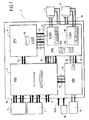
- Processor 1 has internal buses 13 and external buses 14 making respectively communicate with each other the units and peripherals which have just been mentioned.
- a clock 15 cadences operations.
- the address generation unit 6 includes a data manipulation unit 16 formed of two groups of registers 16a and 16b (see also Figure 2) called of general application, which cooperate respectively with memories 7 and 8 with which they can exchange data during the execution of the program.
- the registers of general application 16a and 16b can also be used as temporary registers during data transfers between the various processor units 1 and memories 7 and 8. They can also contain operands for the unit of data processing 9.
- the processor 1 uses, as known per se, a double addressing which allows access in parallel to two values stored in memory or in registers which are simultaneously applied to registers and at DPU 9. For example, the two values can be multiplied and the result of multiplication may be transferred to a planned accumulation register in the data processing unit 9. It is for this reason that the processor 1 includes the two data memories 7 and 8 and, consequently, the unit address development includes two address development devices working in parallel and designated respectively by the references 17 and 18, these devices, being also called X AGU and Y AGU (AGU for Address Generation Unit), are designed in accordance with essential features of the invention. However, a device address generation according to the invention can also be useful in a processor designed to work with simple addressing.
- Devices 17 and 18 are used to generate addresses allowing to indirectly access their associated memory 7 or 8 via registers. As they have an identical structure, we will only describe one, in this case the device 17.
- the fifth ix0w group of registers includes four so-called registers extended instructions designated respectively by ix0, ix1, ix2 and ix3.
- the registers of the sets 16a and 16b are numbered respectively from rx0 to rx7 or from ry0 to ry7 when they contain a single word from rx0w to rx7w or ry0w to ry7w when they contain four words of data at a time, the use of the number of words being optional (function of the program) and dependent on the algorithms to be executed by processor 1.
- the width of the registers which just described corresponds to the width of the data words used in the processor 1, a width of 24 bits being preferred, with the exception of that of the registers of configuration cx0 to cx3 which preferably have a width of 20 bits.
- Table 1 below shows an example of what a configuration register among the registers cx0 to cx3 can contain, while Figure 3 shows the distribution of the fields and an example of the content of such a register, this being referenced cx / yn signifying that it is a configuration register n among four configuration registers respectively for the XAGU and YAGU units.
- Figure 3 also indicates that all the fields can work in read / write. Writing can be done by program instructions specially provided for this purpose and intended to modify, as necessary, the content of the register concerned. In addition, all the positions of the register can be reset to the value "O".
- the value C (in hexadecimal) of the PRO field means that the address will be determined by the sum of the contents of the index register an and the value on of the associated offset register multiplied by the value % mn of the associated modulo register.
- the value F of the field PRO means that the address will be equal to the value of the register index year plus the content of the OFFA field.
- Table 2 below shows an example of what a register of extended instructions can contain among registers ix0 to ix3, while Figure 4 shows the distribution of fields and a possible example of the content of fields in such a register .
- the extended instruction register represented in FIG. 4 is referenced ix / yn signifying that it is an n register among four extended instruction registers for the XAGU and YAGU units respectively.
- Figure 4 also indicates that all the fields can work in read / write.
- writing can be carried out by program instructions specially provided for this purpose and intended to modify, as required, the content of the register concerned.
- certain positions of the register can be reset to the value "O".
- FIG. 5 shows a detailed diagram of the address generation unit 17 (XAGU), it being recalled that the address development unit 18 (YAGU) has the same structure. The latter will therefore not be described in detail.
- Program instruction from sequencing unit 2 is assumed be placed in a register 20, comprising a field in which the part is loaded instructions containing the CE address generation code used in the device according to the invention.
- the register 20 can contain the remaining part PR of the instructions (not shown), usually much larger than that of the CE address development code, one instruction can be defined in total on 32 bit for example.
- the CE address development code presents a range of six bits numbered from b1 to b6. The address development system 17 therefore only uses six bits of an instruction to operate.
- the PR part not assigned to address development includes two DRAG bits for designating registers of general application allowing select from a set of registers, a register of general application rx0 to rx3 or rx0w to rx3w (in the narrow or wide version) via a line 21.
- Two bits b1 and b2 of the CE address generation code are transferred by a line 25 to a multiplexer 22 which thus makes it possible, depending on the value of the two bits, to choose which of the four index or address registers ax0 to ax3 and their offset registers, of modulo and configuration respectively associated, will be used for the elaboration of a address at a given point in time during the program.
- Multiplexer 22 places the continuous registers chosen in a temporary register 23 via a line 24.
- Two other bits b3 and b4 of the address generation code appearing on a line 26 are intended to define operations which will be executed for the calculation Address. The control process initiated by these bits will be explained later.
- Another bit b5 appearing on a line 27 defines the alternative between a basic operation or a predefined operation on the one hand and an extended operation on the other share, all these operations being implemented in an address calculation circuit 28 to wired logic which applies these operations to the contents of index registers and registers offset and modulo associates selected via multiplexer 22 and placed in register 23.
- the address calculated in circuit 28 is used directly for addressing memory 7.
- a last bit b6 of the address development code appearing on a line 29 defines the alternative between a predefined operation and an extended operation.
- bits b3 and b4 also positions two multiplexers 31 and 32.
- the multiplexer 31 is intended for selecting a field from the three fields PR0, PR1 and PR2 defining predefined operations forming part of the content of a register of configuration cx0 to cx3, the codes of these fields being transferred respectively to the lines 33, 34 and 35.
- the output of the multiplexer 31 constitutes one of the inputs of the multiplexer 30.
- bit b5 is applied to the control input of multiplexer 30 and to that of another multiplexer 36 of which it also constitutes one of the inputs.
- the other entry of this multiplexer is made up of the value of bit b6, which also forms one of the inputs of the multiplexer 30.
- the multiplexer 32 is intended to select the content of one of the registers extended instructions ix0 to ix3 depending on the value of bits b3 and b4. This content is placed in a temporary register 37 which transfers it to a circuit 38 for multiplexing and transcoding positioned by the output of the multiplexer 36. This circuit forms the signal of operation with which the address calculation circuit 28 must work.
- the bit in the W field (see table 1) of the configuration registers cx0 to cx3 is transferred via register 23 and a line 39 to a circuit 40 of determination of narrow or wide data words. This circuit is connected to both general and memory registers 7.
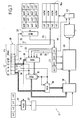
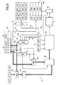
- the unit 17 can thus operate in three different modes which are respectively illustrated in figures 6, 7 and 8 and which are the basic mode, the predefined mode and the mode extended. We will now successively examine these operating modes, being understood that the circulation of various types of information appears in large double lines identified each time by a particular hatching.
- the operation code of the calculation implemented in the calculation circuit 28 is contained directly in the address development code of program instruction. These are the seven basic operations and the NOP code (not bits) define bits b3, b4 and b6. Multiplexers 30 and 36 are then transparent by the value of these three bits under the control of bit b5. The code of operation is applied to the multiplexing and transcoding circuit 38 which is also transparent for this code by applying the value of bit b5. The operation code of base is therefore applied to the calculation circuit 28 which performs the calculation on the contents of index, offset and modulo registers stored in temporary register 23 at the time considered. These contents were selected by the value of bits b1 and b2 positioning the multiplexer 22.
- FIG. 7 represents the execution of an address calculation using a code of predefined operation.
- the multiplexing and transcoding circuit 38 is transparent for the input coming from the multiplexer 30 via the value of the bit b6 which passes through the multiplexer 36 positioned by the value of bit b5.
- bits b3 and b4 chooses one of the predefined operations in the register of configuration cxn selected via multiplexer 22 and placed in the corresponding field in the temporary register 23.
- the corresponding code crosses the multiplexers 31 and 30.
- the multiplexing and transcoding circuit 38 is transparent for the content of the temporary register 37 in which the content of one of the extended registers ix0 to ix3 through the multiplexer 32.
- the latter is positioned by the value of bits b3 and b4.
- the transparency of circuit 38 is ensured, as in the case of FIG. 7 via the value of bit b5 which transmits the value of bit b6 to this circuit 38.
- the address calculation circuit 28 will work with the instruction defined in the selected extended register using the codes specified as an example in table 2 above.
- each program instruction needs only six bits to which functions are assigned doubles.
- bits b3, b4 and b6 are used both to define the code value of operation in the basic mode and for positioning multiplexers in the device address development.
- the more complex operations for calculating addresses are defined using dedicated registers such as configuration registers and extended instructions, which gives great flexibility to the possibilities of programming, despite the low number of bits which in the program instruction define the address development code.
- the contents the registers in question may be replaced at any time by other content in the according to the needs of the execution of the algorithms.
Landscapes
- Engineering & Computer Science (AREA)
- Software Systems (AREA)
- Theoretical Computer Science (AREA)
- Physics & Mathematics (AREA)
- General Engineering & Computer Science (AREA)
- General Physics & Mathematics (AREA)
- Executing Machine-Instructions (AREA)
Abstract
Description
- l'opération arithmétique à effectuer,
- dans quel registre le résultat doit être placé,
- la désignation du registre d'adressage adéquat pour la mémoire 1,
- l'opération à effectuer sur le contenu de ce registre d'adressage,
- la désignation du registre d'offset adéquat,
- la désignation du registre de modulo adéquat,
- la désignation d'un autre registre d'adressage adéquat pour la mémoire 2,
- l'opération à effectuer sur le contenu de cet autre registre d'adressage,
- la désignation du registre d'offset adéquat à associer à cet autre registre,
- la désignation du registre de modulo adéquat à associer à cet autre registre,
- faible nombre d'opérations arithmétiques,
- faible nombre de registres de stockage
- faible nombre de registres d'adressage,
- faible nombre d'opérations sur les registres d'adressage,
- sélection figée des registres d'offset et de modulo associés de façon non modifiable à leur registre d'adressage.
- la figure 1 est schéma symbolique de l'architecture générale d'un processeur DSP dans lequel le procédé selon l'invention peut être mis en oeuvre;
- la figure 2 est une représentation symbolique de certains registres et jeux de registres utilisés dans le processeur DSP de la figure 1;
- les figures 3 et 4 montrent la répartition des champs de certains registres illustrés sur la figure 2;
- la figure 5 est un schéma symbolique d'une unité d'élaboration d'adresses utilisée dans le processeur DSP de la figure 1; et
- les figures 6 à 8 sont des schémas symboliques similaires à celui de la figure 5 et montrant la circulation des informations dans trois modes spécifiques d'élaboration d'adresses.
- un registre d'adresses de base ou registre d'index désigné respectivement par ax0, ax1, ax2 et ax3. Ils sont destinés à contenir l'adresse de mémoire de données à laquelle il sera accédé dans le cas d'un accès indirect à la mémoire de données 7.
- un registre d'incrément/décrément dit d'offset désigné respectivement par ox0, ox1, ox2, ox3. Ils contiennent la valeur d'incrément/décrément de l'adresse de base, lorsque celle-ci doit être modifiée ultérieurement au cours de l'exécution du programme.
- un registre modulo désigné respectivement par mx0, mx1, mx2, mx3. Ces registres permettent de spécifier une valeur modulo associée à une adresse modifiée ultérieurement lorsqu'il s'agit d'exécuter une adresse indirecte de mémoire de données impliquant une modification d'adresse ultérieure.
- un registre dit de configuration désigné respectivement par cx0, cx1, cx2 et cx3. Ces registres sont utilisés pour configurer les opérations d'accès indirect à la mémoire de données 7 pour les index correspondants.
| CHAMP | FONCTION | BIT/ CHAMP | DESCRIPTION | |||
| PR0 | Opération Prédéfinie | 4 bits | 0 | an=an+1 (sam) | 1 | an=an-1 (sam) |
| 2 | an=an+on (sam) | 3 | an=an-on (sam) | |||
| 4 | an=(an+on)%mn (sam) | 5 | an=(an-on)%mn (sam) | |||
| 6 | addr=an+on,an=an+on | 7 | an=an+OFFA (sam) | |||
| 8 | addr=an, an=an+1 | 9 | addr=an·1, an=an-1 | |||
| A | addr=an, an=an+on | B | addr=an, an=an·on | |||
| C | addr=an, an=(an+on)%mn | D | addr=an, an=(an-on)%mn | |||
| E | addr=an | F | addr=an, an=an+OFFA | |||
| PR1 | Opération prédéfinie | 4 bits | 0 | an=an+1 (sam) | 1 | an=(an+1)%mn (sam) |
| 2 | an=an+on (sam) | 3 | an=(an+1)%mn+OFFA(sam=) | |||
| 4 | an(an+on)%mn (s.am) | 5 | an=(an+on)%mn+OFFA (sam) | |||
| 6 | addr=an+on, an=an+on | 7 | an=an+OFFA)%mn+1 (sam) | |||
| 8 | addr=an, an=an+1 | 9 | addr=an, an=(an+1)%mn | |||
| A | addr=an, an=an+on | B | addr=an, an=(an+1 )%mn+OFFA | |||
| C | addr=an, an(an+on)%mn | D | addr=an, an=(an+on)%mn+OFFA | |||
| E | addr=an | F | addr=an, an=(an+OFFA)%mn+1 | |||
| PR2 | Opération prédéfinie | 4 bits | 0 | an=an+1 (sam) | 1 | an=(an+1)%mn (s.a.m.) |
| 2 | an=an+OFFA (sam) | 3 | an=(an+1)%mn+OFFA (sam) | |||
| 4 | an=(an+OFFA)%mn (sam) | 5 | an=(an+on)%mn+OFFA (sam) | |||
| 6 | addr=an+OFFA, an=an+OFFA | 7 | an=(an+OFFA)%mn+1 (sam) | |||
| 8 | addr=an, an=an+1 | 9 | addr=an; an=(an+1)%mn | |||
| A | addr=an, an=an+OFFA | B | addr=an, an=(an+l)%mn+OFFA | |||
| C | addr=an, an=(an+OFFA)%mn | D | addr=an, an=(an+on)%mn+OFFA | |||
| E | addr=an | F | addr=an, an=(an+OFFA)%mn+1 | |||
| OFFA | OFFset B N'est utilisée qu'avec une opération étendue | 3 bits | 0 | 1 | 1 | 2 |
| 2 | 3 | 3 | 4 | |||
| 4 | -4 | 5 | -3 | |||
| 6 | -2 | 7 | -1 | |||
| W | Transfert de Données Mémoire larges | 1 bit | 0 | Mot Etroit | 1 | Mot Large |
- an le contenu du registre d'adresse à engendrer,
- on le registre d'offset associé au registre de configuration concerné,
- %mn le registre modulo associé au registre de configuration concerné,
- sam sans accès mémoire
| CHAMP | FONCTION | BITS | DESCRIPTION | |||
| PREAD | Élaboration d'adresse prémodifiée pour accès à la mémoire courant; partie de l'instruction | 3 bits | 0 | addr=axlyn | 1 | addr= ax|yn+OFFB |
| 2 | addr= ax|yn+MR1 | 3 | addr= ax|yn-MR1 | |||
| 4 | addrMSB=ax|yn MSB, addrLSB=shr(ax|yn LSB) LSB=log2(MR)->addrlog2(MR)=C | 5 | addr= ax|yn+OR | |||
| 6 | addr= ax|yn-OR | 7 | ||||
| POSAD1 | Elaboration d'adresse postmodifiée; Première partie de l'instruction étendue | 4 bits | 0 | RES1= ax|yn+MR1 | 1 | RES1= ax|yn-MR1 |
| 2 | RES1= ax|yn+OR | 3 | RES1= ax|yn-OR | |||
| 4 | RES1=ax|yn+MR2 | 5 | RES1= ax|yn-MR2 | |||
| 6 | RES1= ax|yn+OFFB | 7 | "0" | |||
| 8 | RES1=(ax|yn+OR)%MR1 | 9 | RES1=(ax|yn- | |||
| A | RES1=(ax|yn+OFFB)%MR1 | B | addrMSB= ax|yn MSB, addrLSB =0 LSB=log2(MR) | |||
| C | RES1=(ax|yn+1)%MR1 | D | RES1=(ax|yn- | |||
| E | ax|yn+RCS | F | OR+RCS | |||
| POSAD2 | Elaboration d'adresse postmodifiée; Deuxième partie de l'instruction étendue | 4 bits | O | RES2=RES1+1 | 1 | RES2=RES1-1 |
| 2 | RES2=RES1+OFFB | 3 | RES2=RES1+MR2 | |||
| 4 | RES2=RES1-MR2 | 5 | RES2=RES1+2*MR2 | |||
| 6 | RES2= (MR1,#IMM4) | 7 | RES2= | |||
| 8 | RES2= (RES1,#IMM4) | 9 | RES2= (OR,#lMM4) | |||
| A | RES2=AR | B | RES2=OR | |||
| C | RES2=MR2 | D | RES2=OR+MR2 | |||
| E | RES2=OR+OFFB | F | RES2=MR2+OFFB | |||
| POSTR1 | Registre de destination de POSAD2-RES2 | 2 bits | 0 | 1 | ax|yn=RES1 | |
| 2 | OR-RES1 | 3 3 | MR2=RES1 | |||
| POSTR2 | Registre de destination POSAD2-RES2 | 2 bits | 0 | MR1=RES2 | 1 | ax|yn=RES2 |
| 2 | OR+RES2 | 3 | MR2=RES2 | |||
| OR | Registre d'offset ox/yn | 2 bits | 0 | ox|y0 | 1 | ox|y1 |
| 2 | ox|y2 | 3 | ox|y3 | |||
| MR1/2 | Registre modulo mx/yn | 2bits | 0 | mx|y0 | 1 | mx|y1 |
| 2 | mx|y2 | 3 | mx|y3 | |||
| OFFB | Offset (-64... +64) | 7 bits | 0 | 1 | 1 | 2 |
| 2 | 3 | 3 | 4 | |||
| 4 | -4 | 5 | -3 | |||
| 6 | -2 | 7 | -1 | |||
| RCR | Sélection du radix de retenu inverse | 2 bits | 0 | radix-2 | 1 | radix-4 |
| 2 | Réservé | 3 | Réservé | |||
| RCS | Dimension d'intervalle de retenu inverse radix-2/radix-4 | 3 bits | 0 | Dimension d'intervalle 24/24 | 1 | Dimension d'intervalle 25/26 |
| 2 | Dimension d'intervalle 26/28 | 3 | Dimension d'intervalle 27/210 | |||
| 4 | Dimension d'intervalle 28/212 | 5 | Dimension d'intervalle 29/214 | |||
| 6 | Dimension d'intervalle 210/216 | 7 | Dimension d'intervalle 211/218 |
Claims (10)
- Dispositif (17, 18) d'élaboration d'adresses pour un processeur DSP (1) destiné à exécuter un programme dont les instructions de programme comprennent un code d'élaboration (CE) des adresses pour l'accès à au moins une mémoire (7, 8) associée à ce processeur (1), ce dispositif (6) comprenant:et des moyens de commande (22, 30, 31, 36, 38) qui en fonction dudit code d'élaboration, assurent sélectivement les transferts des contenus desdits registres et dudit code d'opération vers ledit circuit de calcul (28),un jeu de registres d'adresse (ax0 à ax3; ay0 à ay3), associés chacun, le cas échéant, à un registre d'offset (ox0 à ox3; oy0 à oy3) et/ou à un registre de modulo (mx0 à mx3; my0 à my3),un circuit de calcul d'adresses (28) qui sur la base de codes d'opération chaque fois désignés par le code d'élaboration d'adresses (CE) des instructions et du contenu d'un registre d'adresse (ax0 à ax3; ay0 àay3) et éventuellement de ses registres associés (0x0 à ox3; oy0 à oy3; mx0 à mx3; my0 à my3), sélectionné parmi lesdits registres d'adresse, calcule chaque adresse d'accès à ladite mémoire (7, 8),chaque code d'élaboration (CE) de chaque instruction définissant l'un desdits codes d'opération à envoyer audit circuit de calcul (28) et désignant le registre d'adresse dont le contenu doit subir cette opération de calcul,
caractérisé en ce que chacun desdits registres d'adresse (ax0 à ax3; ay0 à ay3) est associé en outre à un registre de configuration (cx0 à cx3; cy0 à cy3) qui est désigné en même temps que ce registre d'adresse par ledit code d'élaboration d'adresses (CE),
en ce que chacun desdits registres de configuration (cx0 à cx3; cy0 à cy3) contient au moins un jeu de codes d'opération prédéfinis(O à F), chaque code d'opération étant à même de commander une opération de calcul prédéterminée dans ledit circuit de calcul (28), et
en ce que lesdits moyens de commande (22, 30, 31, 36, 38) sont agencés pour transférer sélectivement, en fonction de la valeur d'au moins un premier bit (b3, b4) dudit code d'élaboration d'adresses, lesdits codes d'opération prédéfinis vers lesdits moyens de calcul (28). - Dispositif selon la revendication 2, caractérisé en ce que chaque registre de configuration (cx0 à cx3; cy0 à cy3) comprend une pluralité de champs contenant chacun un jeu de codes d'opération.
- Dispositif selon la revendication 2, caractérisé en ce que chaque registre de configuration (cx0 à cx3; cy0 à cy3) comprend trois champs contenant chacun un jeu de codes d'opération et en ce que les codes d'opération sont définis sur quatre bits.
- Dispositif selon l'une quelconque des revendications 1 à 3, caractérisé en ce qu'il comprend en outre un jeu de registres d'instructions étendues (ix0 à ix3; iy0 à iy3) pour permettre sélectivement l'exécution d'opérations complexes de calcul d'adresses dans ledit circuit de calcul d'adresses (28) et
en ce que lesdits moyens de commande (22, 30, 31, 36, 38) sont également agencés pour,en fonction d'un second bit (b6) prédéterminé dudit code d'élaboration d'adresses (CE) desdites instructions de programme, transférer vers ledit circuit de calcul d'adresses (28), soit un code d'opération contenu dans l'un desdits registres de configuration (cx0 à cx3, cy0 à cy3) pour mettre en oeuvre une opération prédéfinie de calcul d'adresse, soit le contenu de l'un desdits registres d'instructions étendues (ix0 à ix3; iy0 à iy3) pour mettre en oeuvre une opération de calcul complexe défini par ce contenu, eten fonction, d'au moins un troisième bit (b3, b4) prédéterminé desdites instructions de programme, désigner l'un des registres d'instructions étendues dudit jeu de registres d'instructions étendues (ix0 à ix3; iy0 à iy3). - Dispositif selon les revendications 2 et 4, caractérisé en ce que lesdits premier et troisième bits (b3, b4) dudit code d'élaboration d'adresses (CE) occupent la même position dans ladite instruction de programme et sont utilisés pour désigner, en fonction de la valeur dudit second bit (b6), soit les champs desdits registres de configuration (cx0 à cx3, cy0 à cy3), soit un registre d'instructions étendues dans ledit jeu de registres d'instructions étendues (ix0 à ix3; iy0 à iy3).
- Dispositif selon l'une quelconque des revendications précédentes, caractérisé en ce que lesdits moyens de commande (22, 30, 31, 36, 38) sont également agencés pour, en fonction de la valeur d'au moins un quatrième bit (b5) dudit code d'élaboration d'adresses (CE) appliqué audit circuit de calcul d'adresses (28), un code d'opération d'adresse désignant une pluralité d'opérations de calcul fréquentes lors de l'exécution dudit programme.
- Dispositif selon les revendications précédentes prises ensemble, caractérisé en ce que lesdites opérations de calcul fréquentes sont définies par ledit premier (ou troisième; b3, b4) bit et ledit second bit (b6).
- Dispositif selon la revendication 5, caractérisé en ce que le code d'élaboration d'adresse (CE) contient deux bits (b3, b4) pour la sélection desdits registres de configuration et desdits registres d'instructions étendues.
- Dispositif selon l'une quelconque des revendications 1 à 8, pour un processeur DSP pouvant fonctionner sélectivement dans des modes de mots de données étroits et larges, ces mots de données pouvant être stockés temporairement dans au moins un jeu de registres d'application générale (rx0 à rx3; rx0w à rx3w; ry0 à ry3; ry0w à ry3w), caractérisé en ce que chacun desdits registres de configuration (cx0 à cx3, cy0 à cy3) comprend un champ définissant l'un ou l'autre de ces modes de mots de données.
- Processeur DSP comprenant au moins un dispositif d'élaboration d'adresses (17, 18) selon l'une quelconque des revendications 1 à 9.
Priority Applications (2)
| Application Number | Priority Date | Filing Date | Title |
|---|---|---|---|
| EP02291405A EP1369774A1 (fr) | 2002-06-06 | 2002-06-06 | Dispositif d'élaboration d'adresses pour un processeur de signaux numériques |
| US10/455,808 US7213127B2 (en) | 2002-06-06 | 2003-06-06 | System for producing addresses for a digital signal processor |
Applications Claiming Priority (1)
| Application Number | Priority Date | Filing Date | Title |
|---|---|---|---|
| EP02291405A EP1369774A1 (fr) | 2002-06-06 | 2002-06-06 | Dispositif d'élaboration d'adresses pour un processeur de signaux numériques |
Publications (1)
| Publication Number | Publication Date |
|---|---|
| EP1369774A1 true EP1369774A1 (fr) | 2003-12-10 |
Family
ID=29433216
Family Applications (1)
| Application Number | Title | Priority Date | Filing Date |
|---|---|---|---|
| EP02291405A Withdrawn EP1369774A1 (fr) | 2002-06-06 | 2002-06-06 | Dispositif d'élaboration d'adresses pour un processeur de signaux numériques |
Country Status (2)
| Country | Link |
|---|---|
| US (1) | US7213127B2 (fr) |
| EP (1) | EP1369774A1 (fr) |
Families Citing this family (2)
| Publication number | Priority date | Publication date | Assignee | Title |
|---|---|---|---|---|
| US7877571B2 (en) * | 2007-11-20 | 2011-01-25 | Qualcomm, Incorporated | System and method of determining an address of an element within a table |
| US9304899B1 (en) * | 2012-08-24 | 2016-04-05 | Altera Corporation | Network interface circuitry with flexible memory addressing capabilities |
Citations (3)
| Publication number | Priority date | Publication date | Assignee | Title |
|---|---|---|---|---|
| US5918253A (en) * | 1994-01-28 | 1999-06-29 | Ricoh Company, Ltd. | Memory address generator |
| US6038584A (en) | 1989-11-17 | 2000-03-14 | Texas Instruments Incorporated | Synchronized MIMD multi-processing system and method of operation |
| WO2001098893A1 (fr) * | 2000-06-19 | 2001-12-27 | Koninklijke Philips Electronics Nv | Generation d'adresses de memoire a l'aide de registres de regles |
Family Cites Families (13)
| Publication number | Priority date | Publication date | Assignee | Title |
|---|---|---|---|---|
| US5450553A (en) * | 1990-06-15 | 1995-09-12 | Kabushiki Kaisha Toshiba | Digital signal processor including address generation by execute/stop instruction designated |
| US5678037A (en) * | 1994-09-16 | 1997-10-14 | Vlsi Technology, Inc. | Hardware graphics accelerator system and method therefor |
| US5659700A (en) * | 1995-02-14 | 1997-08-19 | Winbond Electronis Corporation | Apparatus and method for generating a modulo address |
| US6163836A (en) * | 1997-08-01 | 2000-12-19 | Micron Technology, Inc. | Processor with programmable addressing modes |
| US6209076B1 (en) * | 1997-11-18 | 2001-03-27 | Intrinsity, Inc. | Method and apparatus for two-stage address generation |
| US6567910B2 (en) * | 1998-02-13 | 2003-05-20 | Texas Instruments Incorporated | Digital signal processing unit with emulation circuitry and debug interrupt enable register indicating serviceable time-critical interrupts during real-time emulation mode |
| US6105126A (en) * | 1998-04-30 | 2000-08-15 | International Business Machines Corporation | Address bit decoding for same adder circuitry for RXE instruction format with same XBD location as RX format and dis-jointed extended operation code |
| US6401196B1 (en) * | 1998-06-19 | 2002-06-04 | Motorola, Inc. | Data processor system having branch control and method thereof |
| US6363469B1 (en) * | 1998-07-13 | 2002-03-26 | Matsushita Electric Industrial Co., Ltd. | Address generation apparatus |
| US6539467B1 (en) * | 1999-11-15 | 2003-03-25 | Texas Instruments Incorporated | Microprocessor with non-aligned memory access |
| US6453405B1 (en) * | 2000-02-18 | 2002-09-17 | Texas Instruments Incorporated | Microprocessor with non-aligned circular addressing |
| US6457115B1 (en) * | 2000-06-15 | 2002-09-24 | Advanced Micro Devices, Inc. | Apparatus and method for generating 64 bit addresses using a 32 bit adder |
| US6647484B1 (en) * | 2000-09-19 | 2003-11-11 | 3 Dsp Corporation | Transpose address mode in general purpose DSP processor |
-
2002
- 2002-06-06 EP EP02291405A patent/EP1369774A1/fr not_active Withdrawn
-
2003
- 2003-06-06 US US10/455,808 patent/US7213127B2/en not_active Expired - Fee Related
Patent Citations (3)
| Publication number | Priority date | Publication date | Assignee | Title |
|---|---|---|---|---|
| US6038584A (en) | 1989-11-17 | 2000-03-14 | Texas Instruments Incorporated | Synchronized MIMD multi-processing system and method of operation |
| US5918253A (en) * | 1994-01-28 | 1999-06-29 | Ricoh Company, Ltd. | Memory address generator |
| WO2001098893A1 (fr) * | 2000-06-19 | 2001-12-27 | Koninklijke Philips Electronics Nv | Generation d'adresses de memoire a l'aide de registres de regles |
Also Published As
| Publication number | Publication date |
|---|---|
| US20040034758A1 (en) | 2004-02-19 |
| US7213127B2 (en) | 2007-05-01 |
Similar Documents
| Publication | Publication Date | Title |
|---|---|---|
| JP7074363B2 (ja) | 準同型暗号下での安全な計算を加速するための準同型処理ユニット(hpu) | |
| EP1414182B1 (fr) | Masquage de données décomposées dans un système de résidus | |
| EP1619589B1 (fr) | Procédé de programmation d'un contrôleur de DMA dans un système sur puce et système sur puce associé | |
| FR2613093A1 (fr) | Systeme de calcul a adressage independant du mode d'exploitation | |
| FR2588980A1 (fr) | Processeur de traitement de signal numerique comportant plusieurs multiplicateurs | |
| TWI507982B (zh) | 向量算術縮減 | |
| EP3803636B1 (fr) | Processeur ntt incluant une pluralite de bancs de memoires | |
| US9223752B2 (en) | Digital signal processor with one or more non-linear functions using factorized polynomial interpolation | |
| EP1617335A1 (fr) | Procédé de programmation d'un contrôleur de DMA dans un système sur puce et système sur puce associé | |
| CN108958848A (zh) | 近存储器计算体系结构 | |
| FR2595474A1 (fr) | Dispositif de controle et de verification du fonctionnement de blocs internes a un circuit integre | |
| EP1125205B1 (fr) | Memoire a acces vectoriel | |
| EP1830264A1 (fr) | Procédé et dispositif de sauvegarde et de restauration d'une manière interruptible d'un ensemble de registres d'un microprocesseur | |
| FR2637708A1 (fr) | Dispositif pour le traitement de donnees | |
| FR3076925A1 (fr) | Fonction cryptographique | |
| CN111381905B (zh) | 一种程序处理方法、装置及设备 | |
| EP0043745B1 (fr) | Système de traitement et de mémorisation de données numériques, notamment pour tomodensitomètre | |
| FR2662281A1 (fr) | Processeur comprenant un fichier de registres adressables en plusieurs jeux de registres contenus dans des fenetres. | |
| JP3683598B2 (ja) | データ駆動型情報処理装置 | |
| TWI320906B (en) | Method for allocating registers for a processor | |
| EP3814893B1 (fr) | Accès mémoire de processeurs | |
| Caffarena et al. | High-level synthesis of multiple word-length DSP algorithms using heterogeneous-resource FPGAs | |
| KR100879896B1 (ko) | 밴드 인터리브 포맷으로부터 밴드 분할 포맷으로의 포맷변환 장치 | |
| US20240220255A1 (en) | Data parallelism | |
| EP1821197A2 (fr) | Dispositif de traitement en notation polonaise inversée, et circuit intégré électronique comprenant un tel dispositif de traitement |
Legal Events
| Date | Code | Title | Description |
|---|---|---|---|
| PUAI | Public reference made under article 153(3) epc to a published international application that has entered the european phase |
Free format text: ORIGINAL CODE: 0009012 |
|
| AK | Designated contracting states |
Kind code of ref document: A1 Designated state(s): AT BE CH CY DE DK ES FI FR GB GR IE IT LI LU MC NL PT SE TR |
|
| AX | Request for extension of the european patent |
Extension state: AL LT LV MK RO SI |
|
| 17P | Request for examination filed |
Effective date: 20040120 |
|
| AKX | Designation fees paid |
Designated state(s): CH DE DK FR GB LI |
|
| 17Q | First examination report despatched |
Effective date: 20081028 |
|
| GRAP | Despatch of communication of intention to grant a patent |
Free format text: ORIGINAL CODE: EPIDOSNIGR1 |
|
| GRAJ | Information related to disapproval of communication of intention to grant by the applicant or resumption of examination proceedings by the epo deleted |
Free format text: ORIGINAL CODE: EPIDOSDIGR1 |
|
| GRAP | Despatch of communication of intention to grant a patent |
Free format text: ORIGINAL CODE: EPIDOSNIGR1 |
|
| INTG | Intention to grant announced |
Effective date: 20180227 |
|
| INTG | Intention to grant announced |
Effective date: 20180312 |
|
| GRAJ | Information related to disapproval of communication of intention to grant by the applicant or resumption of examination proceedings by the epo deleted |
Free format text: ORIGINAL CODE: EPIDOSDIGR1 |
|
| GRAP | Despatch of communication of intention to grant a patent |
Free format text: ORIGINAL CODE: EPIDOSNIGR1 |
|
| INTG | Intention to grant announced |
Effective date: 20180420 |
|
| STAA | Information on the status of an ep patent application or granted ep patent |
Free format text: STATUS: THE APPLICATION IS DEEMED TO BE WITHDRAWN |
|
| 18D | Application deemed to be withdrawn |
Effective date: 20180831 |