EP1367817A1 - Pixel actif CMOS à bruit réduit - Google Patents
Pixel actif CMOS à bruit réduit Download PDFInfo
- Publication number
- EP1367817A1 EP1367817A1 EP03364006A EP03364006A EP1367817A1 EP 1367817 A1 EP1367817 A1 EP 1367817A1 EP 03364006 A EP03364006 A EP 03364006A EP 03364006 A EP03364006 A EP 03364006A EP 1367817 A1 EP1367817 A1 EP 1367817A1
- Authority
- EP
- European Patent Office
- Prior art keywords
- during
- pixel
- amplifier
- phase
- switch
- Prior art date
- Legal status (The legal status is an assumption and is not a legal conclusion. Google has not performed a legal analysis and makes no representation as to the accuracy of the status listed.)
- Withdrawn
Links
- 238000000034 method Methods 0.000 claims abstract description 15
- 230000000295 complement effect Effects 0.000 abstract 1
- 229910044991 metal oxide Inorganic materials 0.000 abstract 1
- 150000004706 metal oxides Chemical class 0.000 abstract 1
- 239000004065 semiconductor Substances 0.000 abstract 1
- 101710170230 Antimicrobial peptide 1 Proteins 0.000 description 21
- 238000010586 diagram Methods 0.000 description 13
- 235000021183 entrée Nutrition 0.000 description 9
- 230000008878 coupling Effects 0.000 description 7
- 238000010168 coupling process Methods 0.000 description 7
- 238000005859 coupling reaction Methods 0.000 description 7
- 238000002347 injection Methods 0.000 description 7
- 239000007924 injection Substances 0.000 description 7
- 230000000630 rising effect Effects 0.000 description 5
- 230000002238 attenuated effect Effects 0.000 description 4
- 230000000903 blocking effect Effects 0.000 description 4
- 230000000694 effects Effects 0.000 description 4
- 101710170231 Antimicrobial peptide 2 Proteins 0.000 description 3
- 230000007423 decrease Effects 0.000 description 3
- 230000008569 process Effects 0.000 description 3
- 230000003068 static effect Effects 0.000 description 3
- 230000007704 transition Effects 0.000 description 3
- 230000002596 correlated effect Effects 0.000 description 2
- 238000005286 illumination Methods 0.000 description 2
- 238000005070 sampling Methods 0.000 description 2
- 230000003595 spectral effect Effects 0.000 description 2
- 230000001276 controlling effect Effects 0.000 description 1
- 230000000875 corresponding effect Effects 0.000 description 1
- 229940082150 encore Drugs 0.000 description 1
- 238000005516 engineering process Methods 0.000 description 1
- 230000007246 mechanism Effects 0.000 description 1
- 230000004048 modification Effects 0.000 description 1
- 238000012986 modification Methods 0.000 description 1
- 230000002688 persistence Effects 0.000 description 1
- 239000002699 waste material Substances 0.000 description 1
Images



Classifications
-
- H—ELECTRICITY
- H04—ELECTRIC COMMUNICATION TECHNIQUE
- H04N—PICTORIAL COMMUNICATION, e.g. TELEVISION
- H04N25/00—Circuitry of solid-state image sensors [SSIS]; Control thereof
- H04N25/60—Noise processing, e.g. detecting, correcting, reducing or removing noise
- H04N25/65—Noise processing, e.g. detecting, correcting, reducing or removing noise applied to reset noise, e.g. KTC noise related to CMOS structures by techniques other than CDS
Definitions
- the invention is in the field of image sensors with CMOS active pixels. It relates more particularly a reduced noise CMOS active pixel.
- CMOS complementary metal-oxide-semiconductor
- a conventional CMOS active pixel essentially comprises a photosensitive element, such as a photodiode, associated with three transistors, a selection transistor for selecting the pixel, a transistor for resetting the electric charge of the photosensitive element and a read transistor for delivering a signal representative of the electric charge of the photodiode before and after resetting the pixel.
- the structure of such an active CMOS pixel is shown in FIG. 1.
- the photosensitive element, denoted PD is represented therein by its capacitance C P.
- a reset transistor MR is connected between a supply terminal VDD and the photosensitive element. This transistor is connected to the photosensitive element at a point called a photosensitive node. This photosensitive node is also connected to the gate of a read transistor MD.
- the drain of the transistor MD is connected to the supply terminal VDD and its source is connected to the drain of a selection transistor MS. Finally, the drain of the transistor MS is connected to an output terminal S of the pixel. To select this pixel, a signal SEL is applied to the gate of the transistor MS.
- CMOS active pixel works in the way next: during a reset phase (RESET signal active), the potential of the element photosensitive is reset to a fixed value V0. Then, under the effect of a light signal, the charge the photosensitive element is changed and the voltage across its terminals then goes from V0 to V0-Vsignal, Vsignal being representative of the number of photons incidents received by the pixel.
- a double process Correlated sampling known as CDS is then used to read the Vsignal value. This process consists in reading the signal at the pixel output before and after reset the pixel then calculate the difference between the two signals to deduce Vsignal.
- This pixel structure has four major drawbacks.
- a first drawback is that the reset phase generates a reset noise in the photosensitive element. This noise is higher the lower the capacity of the photodiode.
- a second drawback is the presence of noise Power. Indeed, there is a direct coupling between the VDD voltage supply source and the photosensitive node through capacity drain-gate of the read transistor. A noise then adds to the noise of reset in the photodiode.
- the use of a MOS transistor as switch to reset the pixel produces an injection of electrical charges into the photodiode: part of the electrical charges forming the channel of the MOS transistor are found, after passage of the transistor in its blocking zone, in the photodiode capacity.
- the voltage variation which the higher the capacity of the photodiode is weak. This phenomenon reduces the voltage excursion of the output signal of a fraction may be relatively large.
- a dragging problem also appears when the reset phase fails to completely erase the information acquired in the photodiode during the previous reading phase.
- the dragging is manifested on a screen by a persistence of the image: the image read then contains a residue of the previous image. This problem arises when uses a tape reset technique limited bandwidth.
- the active pixel CMOS comprises a photodiode PD of capacity C P , an amplifier AMP1 active during the reset phase (READ signal inactive), a follower amplifier AMP2 active during the read phase ( READ signal active), two switches IT1 and IT2 connected in series between the output and inverting input of the amplifier AMP1, and a capacitive element CF of capacity C F connected in parallel with the switch IT1.
- the photodiode PD is connected between a photosensitive node N and the ground.
- the non-inverting input of amplifier AMP1 is connected to an output terminal S of the pixel which receives a reference voltage during the pixel reset phase.
- the follower amplifier AMP2 active during the reading phase is placed between the photosensitive node N and the output terminal S of the pixel.
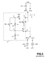
- FIG. 3 A more detailed diagram of this CMOS active pixel is shown in Figure 3.
- a transistor M1 and a M2 line selection transistor are used for train the amplifier AMP1 during the reset. These transistors also form the AMP2 follower amplifier during the reading.
- Transistors M3 and M4 are also used to form switches IT1 and IT2.
- the transistor M1 has its gate connected to the photosensitive node N and its source connected to the output terminal S of the pixel.
- the output terminal S delivers a signal representative of the electric charge of the photodiode during the pixel reading phase.
- the selection transistor M2 is mounted in cascode with the transistor M1, that is to say that its source is connected to the drain of the transistor M1. Its drain is connected to a node B common to all the pixels of the column to which the pixel in question is connected and its gate receives a selection signal SEL to select the pixel.
- the transistor M3, forming the switch IT1 is connected between the photosensitive node N and a point A of the pixel. This transistor is controlled by a reset signal RS1 active during a first period ⁇ 1 of the pixel reset phase.
- the pixel reset phase is in fact made up of three consecutive periods ⁇ 1 , ⁇ 2 and ⁇ 3 .
- the transistor M4 is connected between the node B and the node A. This transistor is controlled by a reset signal RS2 active during the periods ⁇ 1 and ⁇ 2 of the reset phase.
- the capacitive element CF is connected in parallel with the transistor M3 between the node A and the node N. Finally, the sum of the capacitive contributions of each pixel of the column of the pixel considered between its respective point B and the mass is represented on the diagram by a capacity C, connected between node B and ground.
- Means are provided in the image sensor containing the pixel to polarize and feed the pixel during the different operating phases of the pixel. These means are advantageously common to all the pixels of the same column in the image sensor, see all the pixels of the image sensor depending on the case.
- a voltage source VDD and a current source SC1 to supply power to the node B of the pixel respectively during the reading phase and the pixel reset phase.
- a second current source SC2 and a SV voltage source with negligible noise to impose on the pixel output terminal S respectively a current during the reading phase and a reference voltage VREF during the phase of reset.
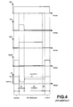
- This active CMOS pixel is illustrated by the timing diagrams of the control signals SEL, RS1, RS2 and READ in figure 4. Reading information contained in the photodiode after modification of its electric charge under the effect of a light signal requires a first reading phase to acquire a signal representative of the illumination of the pixel by the light signal, a reset phase of the electric charge of the pixel, and a second phase of reading to acquire a signal representative of the initial electric charge of the pixel. The difference between these two signals gives a signal representative of the variation of the electric charge due to photons light signal incidents.
- the READ command signal and the SEL selection are active while the RS1 and RS2 are inactive.
- a signal is said to be active if it has a high and inactive voltage level if it has a low voltage level.
- node B is supplied by the supply voltage VDD and a current is imposed by the current source SC2 on the pixel output terminal S.
- the M3 and M4 transistors are blocked.
- the transistor M1 then mounted as a follower, is supplied through the transistor M2.
- a signal from voltage representative of the electric charge of the photodiode is then available on the output terminal S of the pixel.
- the READ signal is inactive.
- control signals SEL, RS1 and RS2 are active.
- the transistors M2, M3 and M4 are therefore conductive.
- the transistor M1 is mounted as an amplifier and its drain is connected to its gate via the transistor M2.
- the pixel is supplied with current from the current source SC1 and the reference voltage VREF is imposed on the output terminal S of the pixel.
- the current supplied by the current source SC1 passes through the transistors M1 and M2 and is absorbed by the voltage source SV.
- a potential VREF + V GS (M1) is imposed on the photosensitive node N, V GS (M1) representing the gate-source voltage of the transistor M1.
- the purpose of the period ⁇ 1 is to erase the information initially contained in the pixel by imposing a fixed voltage across the terminals of the photodiode.
- the control signal RS1 is inactive.
- the transistor M3 is then blocked.
- Noise voltage kT VS F is sampled on the capacitive element CF.
- the transistor M1 is counter-reacted by the capacitive divider formed by the capacitive element CF and the capacitance of the photodiode PD.
- the transistor M1 then operates as an amplifier (amplifier AMP1).
- the transistors M1 and M2 being mounted in cascode, a high static gain is then obtained for the transistor M1.
- the gain of the loop formed by the transistors M1 and M2 and the capacitive divider is high despite the capacitive divider.
- Phase ⁇ 2 must be maintained until the amplifier AMP1 reaches an equilibrium state.
- the RS2 control signal is inactive.
- the transistor M4 is therefore blocked. This transition to a low level is effected very quickly with respect to the time constant of the amplifier AMP1.
- CMOS active pixel structure provides satisfactory results in terms of noise reset, feed noise, injection electric charges in the photodiode and dragging as has been very comprehensively exposed in the French patent application n ° 01/07349 cited previously.
- the gate-drain coupling capacity of transistor M3 produces a positive voltage variation at node B (corresponding to the output of amplifier AMP1) during period ⁇ 2 of the reset phase. This variation is acceptable as long as the amplifier AMP1 does not saturate and does not clip the signal.
- this coupling capacity can be very high.
- the evolution of the potential at node B in this case is shown in Figure 4. As the output of the amplifier is clipped, it no longer amplifies linearly and the desired effect, namely mainly noise correction. reset, is no longer reached.
- the object of the invention is to produce an active pixel Improved CMOS that is insensitive to this problem of capacitive coupling of transistor M3.
- this compensation is provided for modify the structure and functioning of the pixel described above so that the compensation is realized by the transistor M4 and the control signal RS2.
- CMOS active pixel in which the MOS M3 transistors and M4 are arranged in a type configuration parallel rather than series.
- Said first and second amplifiers consist of a first transistor whose gate is connected to the photosensitive node and the source is connected to said reference voltage source during said phase of reset and to a first current source during said reading phase, and a transistor selection controlled by an active selection signal during said reset phases and reading of said pixel, the source of which is connected to the drain of the first transistor and whose drain is connected to a second power source during said reset phase and to a voltage source supply during said reading phase, the source of said first transistor delivering said signal representative of the electric charge of said element photosensitive during said reading phase.
- the transistor forming the second switch is turned on slight inversion just before blocking, to decrease again the reset noise produced by it.
- FIG. 5 The general structure of an active CMOS pixel according to the invention is shown in Figure 5.
- the structure of pixel differs from that shown in Figure 2 by that the IT2 switch is connected in series with the capacitive element CF between the inverting input and the AMP1 amplifier output, and that IT1 switch is connected between input and the output of the amplifier AMP1.
- FIG. 6 A more detailed diagram of the pixel is shown in the figure 6, to compare with that of figure 3.
- the position of the element capacitive CF and transistors M3 and M4 forming the switches IT1 and IT2 is modified.
- the transistor M3 has its drain connected to the node B and its source connected to the photosensitive node N.
- the transistor M4 has its source connected to the photosensitive node N and its drain connected to node A and the capacitive element CF is mounted between the node A and the node B.
- the rest of the diagram is unchanged from Figure 3. Therefore, everything that has been described in the preamble to this application on the CMOS active pixel structure, except for the position of transistors M3, M4 and the element capacitive CF, applies to the present invention.
- control signal SEL, RS1, RS2 and READ of the pixel only the control signal RS2 applied to the gate of the transistor M4 is modified with respect to the timing diagrams of FIG. 4. This signal is active at the start of the period ⁇ 1 of erasure to reset the potential on the capacitive element CF and during most of the relaxation period ⁇ 2 .
- the reading process of the pixel state includes two reading phases separated by a reset phase.
- the first one reading phase aims to produce a signal representative of the electric charge of the photodiode after illumination of the pixel by a light signal;
- the reset phase aims to reset the electric charge of the photodiode and
- the second reading phase aims to produce a signal representative of the initial electric charge of the pixel.
- the difference between the two charges read gives the electric charge due to the incident photons of the light signal.
- the READ command signal and the SEL selection are active while the RS1 and RS2 are inactive.
- the active pixel then works like the pixel in figure 3.
- the READ signal is inactive and the SEL signal remains active.
- the signals RS1 and RS2 are active at the start of phase ⁇ 1 to reset all the potentials of the pixel. Then quickly, the RS2 signal becomes inactive again.
- the transistors M2 and M3 are conductive.
- the transistor M1 is mounted as an amplifier and the drain of the transistor M2 is connected to the gate of the transistor M1.
- a fixed potential VREF + V GS (M1) is imposed on the photosensitive node N to erase the information contained in the photodiode.
- the first important condition for this compensation be effective is to wait for blocking complete of transistor M3 to conduct the transistor M4.
- the transistor M4 then makes it possible to exactly compensate for the electrical charges injected by transistor M3 on the node common to both transistors. This is why the command to close the transistor M4 does not intervene immediately after the opening command of transistor M3 but some nanoseconds after.
- the two transistors M3 and M4 must be matched for compensation to be same amplitude as the voltage variation introduced by the capacitive coupling of transistor M3 to node B, but of opposite sign. This means that the transistors M3 and M4 have the same dimensions, the same geometry and of the same orientation in the integrated circuit forming said CMOS active pixel.
- the potential at node B After the rising edge of the signal RS2, the potential at node B returns to a level close to that which it has when the signal RS1 is active, and the amplifier AMP1 can therefore operate in its linear zone during the relaxation period ⁇ 2 .
- the transistor M3 is blocked during the relaxation period ⁇ 2 .
- Noise voltage kT VS F is sampled on the capacitive element CF.
- the transistor M1 is counter-reacted by the capacitive divider formed by the capacitive element CF and the capacitance of the photodiode PD.
- the transistor M1 then operates as an amplifier (amplifier AMP1).
- the transistors M1 and M2 being mounted in cascode, a high static gain is then obtained for the amplifier.
- the value of the loop gain G b remains high despite the capacitive divider.
- the gain-bandwidth product equal to gm 1 / C, where C represents the load capacity on the node B, is fixed by the choice of the current passing through the transistor M1, namely the current supplied by the current source SC1.
- the relaxation period ⁇ 2 is maintained until the amplifier AMP1 reaches a new state of equilibrium.
- the high loop gain G b means that the reset noise kT VS F sampled in feedback on the capacitive element is distributed for a fraction -1 / G b + 1 on the photodiode, and for a fraction G b / G b + 1 on the drain of transistor M2.
- the noise, denoted B1 introduced by the capacitive element CF in the photodiode is attenuated by the loop gain.
- B1 kT VS F G b +1 ⁇ kT G 0 ⁇ VS F + C P VS F 3/2
- a wideband noise B2 is also produced by the transistor M4. This noise is not counter-reacted by the amplifier because, beyond the gain - bandwidth product, the amplifier AMP1 no longer has gain ( ⁇ 1) and therefore no longer functions as an amplifier. Its spectral density is attenuated by the capacitive divider formed by the capacitive element CF and the capacitance of the photodiode.
- B2 VS F VS F + C P ⁇ kT (C F + C P )
- VS F VS P kT VS P ⁇ VS F VS F + C P
- the transistor M4 strongly contributes to the presence of this noise in the pixel.
- a MOS transistor When a MOS transistor is used in low inversion, it is shown that its noise spectral density is 3 dB lower than it would be in the ohmic zone.
- To put the transistor M4 is weak inversion it suffices to gradually lower the control signal RS2 applied to its gate. When the low inversion state is reached, the transistor M4 can then be completely blocked by a falling edge of the signal RS2.
- B total 2 becomes equal to:
- the noise B1 decreases while the noise B2 increases. It is therefore possible to define a value C F for which the total noise is minimal. In practice, the minimum value of the total noise is much lower than the value of the usual reset noise, namely kT VS P .
- the falling edge of the control signal RS1 causes an injection of charges into the photodiode coming from the transistor M3. This injection is then corrected by the rising edge of the signal RS2 during the relaxation period ⁇ 2 . As a result, the photosensitive node is therefore protected against a large injection of electrical charges.
- the lagging mechanism when the transistors M1, M2 and M3 are conductive during the erasure period ⁇ 1 , a fixed voltage is imposed at low impedance on the photodiode, independent of the initial value contained in the pixel.
- the time constant to reach this state is low, around 50 ns. It follows that, after a few time constants, the initial value of the pixel is completely erased.
Landscapes
- Engineering & Computer Science (AREA)
- Multimedia (AREA)
- Signal Processing (AREA)
- Solid State Image Pick-Up Elements (AREA)
- Transforming Light Signals Into Electric Signals (AREA)
Abstract
Description
- le potentiel sur le noeud photosensible N baisse instantanément; et
- une partie des charges électriques constituant le canal du transistor M3 est injectée dans le noeud N, ce qui contribue à faire baisser encore plus le potentiel du noeud N.
- un premier amplificateur actif pendant ladite phase de réinitialisation et dont les entrées inverseuse et non inverseuse sont respectivement connectées au noeud photosensible et à une source de tension de référence,
- un premier interrupteur connecté entre l'entrée inverseuse et la sortie dudit premier amplificateur, commandé par un premier signal de commande actif pendant une première période de la phase de réinitialisation et inactif pendant des deuxième et troisième périodes de la phase de réinitialisation et pendant la phase de lecture,
- un élément capacitif connecté entre la sortie dudit premier amplificateur et un noeud intermédiaire du pixel,
- un deuxième interrupteur connecté entre le noeud photosensible et le noeud intermédiaire du pixel, commandé par un deuxième signal de commande actif pendant le début de la première période de la phase de réinitialisation et pendant la totalité de la deuxième période de la phase de réinitialisation et inactif pendant le reste de la phase de réinitialisation et pendant la phase de lecture, et
- un second amplificateur monté en suiveur, actif pendant la phase de lecture, dont l'entrée est connectée au noeud photosensible et la sortie délivre un signal représentatif de la charge électrique dudit élément photosensible pendant ladite phase de lecture.
- appliquer, pendant une première période, une tension de référence sur l'entrée non inverseuse dudit amplificateur, relier la sortie dudit amplificateur à son entrée inverseuse en fermant ledit premier interrupteur pendant ladite première période, et appliquer brièvement ladite tension de référence sur les deux bornes dudit élément capacitif en fermant momentanément ledit second interrupteur au début ladite première période pour réinitialiser la charge de celui-ci,
- contre-réactionner, pendant une deuxième période dite de relaxation, la sortie dudit amplificateur sur son entrée inverseuse par ledit élément capacitif de rétroaction en fermant ledit second interrupteur jusqu'à atteindre un état d'équilibre, ledit premier interrupteur étant ouvert; et
- ouvrir, pendant un troisième temps, ledit second interrupteur.
- la figure 1, déjà décrite, représente un pixel actif CMOS classique à 3 transistors,
- la figure 2 représente un schéma d'un autre pixel actif CMOS de l'art antérieur,
- la figure 3 représente un schéma plus détaillé du pixel actif CMOS de la figure 2;
- la figure 4 représente les chronogrammes des signaux de commande du pixel actif CMOS de la figure 3;
- la figure 5 représente un schéma d'un pixel actif CMOS selon l'invention;
- la figure 6 représente un schéma plus détaillé du pixel actif CMOS de la figure 5; et
- la figure 7 représente les chronogrammes des signaux de commande et du potentiel au noeud B du pixel actif CMOS de la figure 6.
- la présence d'une capacité de rétroaction CF nécessaire pour cette phase,
- la montée du potentiel au noeud B due au front descendant du signal RS1 sur la grille du transistor M3 est compensée par le front montant du signal RS2 appliqué sur la grille du transistor M4.


- appliquer, pendant une première période 1, une tension de référence VREF+VGS(M1) sur l'entrée non inverseuse dudit amplificateur AMP1, relier la sortie dudit amplificateur à son entrée inverseuse en fermant ledit premier interrupteur IT1 pendant la période 1, et appliquer brièvement la tension de référence VREF+VGS(M1) sur les deux bornes de l'élément capacitif en fermant momentanément le second interrupteur IT2 au début ladite période 1 pour réinitialiser la charge de celui-ci,
- contre-réactionner, pendant une deuxième période dite de relaxation 2, la sortie dudit amplificateur AMP1 sur son entrée inverseuse par ledit élément capacitif de rétroaction CF en fermant ledit second interrupteur IT2 jusqu'à atteindre un état d'équilibre, ledit premier interrupteur IT1 étant ouvert; et
- ouvrir, pendant un troisième temps 3, ledit second interrupteur IT2.
Claims (9)
- Pixel actif CMOS pour capteur d'image comportant un élément photosensible (PD), tel qu'une photodiode, dont la charge électrique est réinitialisée pendant une phase de réinitialisation et lue pendant une phase de lecture, ledit élément photosensible (PD) étant connecté entre un noeud photosensible (N) et la masse, caractérisé en ce qu'il comporte en outre:un premier amplificateur (AMP1) actif pendant ladite phase de réinitialisation et dont les entrées inverseuse et non inverseuse sont respectivement connectées au noeud photosensible (N) et à une source de tension de référence (SV),un premier interrupteur (IT1) connecté entre l'entrée inverseuse et la sortie dudit premier amplificateur (AMP1), commandé par un premier signal de commande (RS1) actif pendant une première période (1) de la phase de réinitialisation et inactif pendant des deuxième et troisième périodes (2,3) de la phase de réinitialisation et pendant la phase de lecture,un élément capacitif (CF) connecté entre la sortie (B) dudit premier amplificateur (AMP1) et un noeud intermédiaire (A) du pixel,un deuxième interrupteur (IT2) connecté entre le noeud photosensible (N) et le noeud intermédiaire (A) du pixel, commandé par un deuxième signal de commande (RS2) actif pendant le début de la première période de la phase de réinitialisation (1) et pendant la totalité de la deuxième période de la phase de réinitialisation (2) et inactif pendant le reste de la phase de réinitialisation et pendant la phase de lecture, etun second amplificateur (AMP2) monté en suiveur, actif pendant la phase de lecture, dont l'entrée est connectée au noeud photosensible (N) et la sortie (S) délivre un signal représentatif de la charge électrique dudit élément photosensible (PD) pendant ladite phase de lecture.
- Pixel actif CMOS selon la revendication 1, caractérisé en ce que lesdits premier et second amplificateurs (AMP1,AMP2) consistent en un premier transistor (M1) dont la grille est connectée au noeud photosensible (N) et la source est reliée à ladite source de tension de référence (SV) pendant ladite phase de réinitialisation et à une première source de courant (SC2) pendant ladite phase de lecture, et un transistor de sélection (M2) commandé par un signal de sélection actif pendant lesdites phases de réinitialisation et de lecture dudit pixel, dont la source est connectée au drain du premier transistor (M1) et dont le drain est connecté à une seconde source de courant (SC1) pendant ladite phase de réinitialisation et à une source de tension d'alimentation (VDD) pendant ladite phase de lecture, la source dudit premier transistor (M1) délivrant ledit signal représentatif de la charge électrique dudit élément photosensible (PD) pendant ladite phase de lecture.
- Pixel actif CMOS selon la revendication 1 ou 2, caractérisé en ce que, CP désignant la capacité de l'élément photosensible, le rapport CF/CP est très inférieur à 1 et en ce que le gain du premier amplificateur (AMP1) est tel que le produit de ce gain par le rapport CF/(CF+CP) est supérieur à 10.
- Pixel actif CMOS selon l'une des revendications précédentes, caractérisé en ce que lesdits premier et deuxième interrupteurs (IT1.IT2) sont réalisés par des transistors MOS (M3,M4) de mêmes dimensions, de même géométrie et de même orientation.
- Procédé de réinitialisation d'un pixel actif CMOS comportant au moins un élément photosensible (PD) de capacité CP ayant un noeud photosensible, un amplificateur (AMP1) ayant une entrée inverseuse connectée audit noeud photosensible, une entrée non inverseuse et une sortie, un premier interrupteur (IT1) initialement dans un état ouvert connecté entre l'entrée inverseuse et la sortie dudit amplificateur, un élément capacitif (CF) de capacité CF connecté entre la sortie dudit amplificateur et un noeud intermédiaire (A) du pixel, et un second interrupteur (IT2) initialement dans un état ouvert connecté entre le noeud photosensible (N) et le noeud intermédiaire (A), ledit procédé étant caractérisé en ce qu'il comprend les étapes suivantes:appliquer, pendant une première période (1), une tension de référence (VREF+VGS(M1)) sur l'entrée non inverseuse dudit amplificateur (AMP1), relier la sortie dudit amplificateur à son entrée inverseuse en fermant ledit premier interrupteur (IT1) pendant ladite première période (1), et appliquer brièvement ladite tension de référence (VREF+VGS(M1)) sur les deux bornes dudit élément capacitif (CF) en fermant momentanément ledit second interrupteur (IT2) au début ladite première période (1) pour réinitialiser la charge de celui-ci,contre-réactionner, pendant une deuxième période dite de relaxation (2), la sortie dudit amplificateur (AMP1) sur son entrée inverseuse par ledit élément capacitif de rétroaction (CF) en fermant ledit second interrupteur (IT2) jusqu'à atteindre un état d'équilibre, ledit premier interrupteur (IT1) étant ouvert; etouvrir, pendant un troisième temps (3), ledit second interrupteur (IT2).
- Procédé selon la revendication 5, caractérisé en ce que le rapport CF/CP est très inférieur à 1 et en ce que le gain de l'amplificateur est tel que le produit de ce gain par le rapport CF/(CF+CP) est supérieur à 10.
- Procédé selon la revendication 5 ou 6, caractérisé en ce que, au début de la période de relaxation (2), ledit second interrupteur (IT2) est amené dans un état fermé lorsque ledit premier interrupteur (IT1) est dans un état complètement ouvert.
- Procédé selon l'une des revendications 5 à 7, caractérisé en ce que lesdits premier et deuxième interrupteurs (IT1,IT2) sont réalisés par des transistors MOS (M3,M4) de mêmes dimensions, de même géométrie et de même orientation.
- Procédé selon la revendication 8, caractérisé en ce que, en fin de période de relaxation (2), le transistor (M4) formant le deuxième interrupteur (IT2) est mis en faible inversion juste avant son blocage.
Applications Claiming Priority (2)
| Application Number | Priority Date | Filing Date | Title |
|---|---|---|---|
| FR0206068A FR2839841A1 (fr) | 2002-05-17 | 2002-05-17 | Pixel actif cmos a bruit reduit |
| FR0206068 | 2002-05-17 |
Publications (1)
| Publication Number | Publication Date |
|---|---|
| EP1367817A1 true EP1367817A1 (fr) | 2003-12-03 |
Family
ID=29286567
Family Applications (1)
| Application Number | Title | Priority Date | Filing Date |
|---|---|---|---|
| EP03364006A Withdrawn EP1367817A1 (fr) | 2002-05-17 | 2003-05-06 | Pixel actif CMOS à bruit réduit |
Country Status (3)
| Country | Link |
|---|---|
| US (1) | US7126636B2 (fr) |
| EP (1) | EP1367817A1 (fr) |
| FR (1) | FR2839841A1 (fr) |
Families Citing this family (9)
| Publication number | Priority date | Publication date | Assignee | Title |
|---|---|---|---|---|
| US7277129B1 (en) * | 2002-10-31 | 2007-10-02 | Sensata Technologies, Inc. | Pixel design including in-pixel correlated double sampling circuit |
| DE602004028652D1 (de) * | 2003-12-11 | 2010-09-23 | Advasense Technologics 2004 Lt | Erazittern |
| US7372493B2 (en) * | 2004-07-12 | 2008-05-13 | Micron Technology, Inc. | Column-wise clamp voltage driver for suppression of noise in an imager |
| US7777171B2 (en) * | 2008-08-26 | 2010-08-17 | Eastman Kodak Company | In-pixel summing of charge generated by two or more pixels having two reset transistors connected in series |
| US20100271517A1 (en) * | 2009-04-24 | 2010-10-28 | Yannick De Wit | In-pixel correlated double sampling pixel |
| WO2013179597A1 (fr) * | 2012-05-30 | 2013-12-05 | パナソニック株式会社 | Dispositif d'imagerie à semi-conducteurs, procédé de commande associé et dispositif de prise d'image |
| CN108987420B (zh) * | 2017-06-05 | 2023-12-12 | 松下知识产权经营株式会社 | 摄像装置 |
| US10623728B2 (en) * | 2018-07-06 | 2020-04-14 | Stmicroelectronics (Grenoble 2) Sas | Image sensors for advanced driver assistance systems utilizing safety pixels to detect malfunctions |
| US11356654B2 (en) | 2018-08-01 | 2022-06-07 | Stmicroelectronics Asia Pacific Pte Ltd | Image sensors for advanced driver assistance systems utilizing regulator voltage verification circuitry to detect malfunctions |
Citations (2)
| Publication number | Priority date | Publication date | Assignee | Title |
|---|---|---|---|---|
| WO2001022727A1 (fr) * | 1999-09-21 | 2001-03-29 | Pixel Devices International, Inc. | Extraction active de ràz a faible bruit pour capteurs d'image |
| EP1263210A1 (fr) * | 2001-05-28 | 2002-12-04 | STMicroelectronics S.A. | Pixel actif CMOS à bruit reduit |
Family Cites Families (4)
| Publication number | Priority date | Publication date | Assignee | Title |
|---|---|---|---|---|
| JPH05158107A (ja) * | 1991-12-10 | 1993-06-25 | Fuji Film Micro Device Kk | 撮像装置用自動測光装置 |
| US5705807A (en) * | 1994-10-24 | 1998-01-06 | Nissan Motor Co., Ltd. | Photo detecting apparatus for detecting reflected light from an object and excluding an external light componet from the reflected light |
| JP4398095B2 (ja) * | 1998-09-09 | 2010-01-13 | 浜松ホトニクス株式会社 | 固体撮像装置 |
| US6459078B1 (en) * | 2000-12-04 | 2002-10-01 | Pixel Devices International, Inc. | Image sensor utilizing a low FPN high gain capacitive transimpedance amplifier |
-
2002
- 2002-05-17 FR FR0206068A patent/FR2839841A1/fr not_active Withdrawn
-
2003
- 2003-05-06 EP EP03364006A patent/EP1367817A1/fr not_active Withdrawn
- 2003-05-14 US US10/437,741 patent/US7126636B2/en not_active Expired - Lifetime
Patent Citations (2)
| Publication number | Priority date | Publication date | Assignee | Title |
|---|---|---|---|---|
| WO2001022727A1 (fr) * | 1999-09-21 | 2001-03-29 | Pixel Devices International, Inc. | Extraction active de ràz a faible bruit pour capteurs d'image |
| EP1263210A1 (fr) * | 2001-05-28 | 2002-12-04 | STMicroelectronics S.A. | Pixel actif CMOS à bruit reduit |
Also Published As
| Publication number | Publication date |
|---|---|
| FR2839841A1 (fr) | 2003-11-21 |
| US20030214596A1 (en) | 2003-11-20 |
| US7126636B2 (en) | 2006-10-24 |
Similar Documents
| Publication | Publication Date | Title |
|---|---|---|
| EP1263210A1 (fr) | Pixel actif CMOS à bruit reduit | |
| FR2665036A1 (fr) | Circuit pour retarder un signal. | |
| EP0585150A1 (fr) | Circuit de lecture pour mémoire, avec précharge et équilibrage avant lecture | |
| CH633670B5 (fr) | Circuit oscillateur a onde rectangulaire pour la mesure du temps. | |
| EP0028960A1 (fr) | Matrice de détection d'un rayonnement électromagnétique et intensificateur d'images radiologiques comportant une telle matrice | |
| EP2047476A2 (fr) | Circuit de retention de charges pour mesure temporelle | |
| EP2047475A2 (fr) | Circuit de lecture d'un element de retention de charges pour mesure temporelle | |
| FR2485829A1 (fr) | ||
| US20060170491A1 (en) | Optoelectronic sensor | |
| EP0474534B1 (fr) | Circuit à constante de temps réglable et application à un circuit à retard réglable | |
| FR2767977A1 (fr) | Etage de sortie pour pompe de charge faible courant et demodulateur integrant une telle pompe de charge | |
| EP0161215B1 (fr) | Amplificateur à compensation de la tension de décalage d'entrée | |
| FR2722625A1 (fr) | Convertisseur a/n a comparaison multiple utilisant le principe d'interpolation | |
| FR2904464A1 (fr) | Circuit eeprom de retention de charges pour mesure temporelle | |
| EP3819615B1 (fr) | Pixel ir reconfigurable en mode di ou bdi | |
| EP1647091B1 (fr) | Amplificateur de tension a faible consommation | |
| CH639804A5 (fr) | Amplificateur dynamique en technologie cmos. | |
| FR2839841A1 (fr) | Pixel actif cmos a bruit reduit | |
| EP0692907B1 (fr) | Circuit de suppression de courant d'obscurité de photodétecteur | |
| EP0182679B1 (fr) | Dispositif photosensible à transfert de ligne muni d'amplificateurs de contre-réaction | |
| FR2962851A1 (fr) | Capteur d'image | |
| FR2914516A1 (fr) | Circuit electronique amplificateur comprenant une paire differentielle et un systeme de contre-reaction. | |
| EP0883900A1 (fr) | Dispositif et procede de lecture d'une matrice de detecteurs photoniques | |
| FR2866180A1 (fr) | Procede de traitement des informations delivrees par une matrice de pixels actifs d'un capteur offrant une dynamique et un gain etendus, et capteur correspondant. | |
| CA1284359C (fr) | Reseau logique dynamique |
Legal Events
| Date | Code | Title | Description |
|---|---|---|---|
| PUAI | Public reference made under article 153(3) epc to a published international application that has entered the european phase |
Free format text: ORIGINAL CODE: 0009012 |
|
| AK | Designated contracting states |
Kind code of ref document: A1 Designated state(s): AT BE BG CH CY CZ DE DK EE ES FI FR GB GR HU IE IT LI LU MC NL PT RO SE SI SK TR |
|
| AX | Request for extension of the european patent |
Extension state: AL LT LV MK |
|
| 17P | Request for examination filed |
Effective date: 20040520 |
|
| AKX | Designation fees paid |
Designated state(s): FR GB |
|
| REG | Reference to a national code |
Ref country code: DE Ref legal event code: 8566 |
|
| 17Q | First examination report despatched |
Effective date: 20050609 |
|
| GRAP | Despatch of communication of intention to grant a patent |
Free format text: ORIGINAL CODE: EPIDOSNIGR1 |
|
| STAA | Information on the status of an ep patent application or granted ep patent |
Free format text: STATUS: THE APPLICATION IS DEEMED TO BE WITHDRAWN |
|
| 18D | Application deemed to be withdrawn |
Effective date: 20091126 |