EP1367674A1 - OLED area illumination lighting apparatus - Google Patents
OLED area illumination lighting apparatus Download PDFInfo
- Publication number
- EP1367674A1 EP1367674A1 EP03076476A EP03076476A EP1367674A1 EP 1367674 A1 EP1367674 A1 EP 1367674A1 EP 03076476 A EP03076476 A EP 03076476A EP 03076476 A EP03076476 A EP 03076476A EP 1367674 A1 EP1367674 A1 EP 1367674A1
- Authority
- EP
- European Patent Office
- Prior art keywords
- substrate
- light sources
- layer
- oled
- electrodes
- Prior art date
- Legal status (The legal status is an assumption and is not a legal conclusion. Google has not performed a legal analysis and makes no representation as to the accuracy of the status listed.)
- Granted
Links
- 238000005286 illumination Methods 0.000 title claims abstract description 15
- 239000000758 substrate Substances 0.000 claims abstract description 61
- 239000004020 conductor Substances 0.000 claims abstract description 18
- 238000000034 method Methods 0.000 claims description 9
- 239000010410 layer Substances 0.000 description 48
- 239000000463 material Substances 0.000 description 36
- -1 gallium nitride Chemical class 0.000 description 17
- 150000001875 compounds Chemical class 0.000 description 13
- 239000002019 doping agent Substances 0.000 description 10
- 229910052751 metal Inorganic materials 0.000 description 9
- 239000002184 metal Substances 0.000 description 9
- MCJGNVYPOGVAJF-UHFFFAOYSA-N quinolin-8-ol Chemical compound C1=CN=C2C(O)=CC=CC2=C1 MCJGNVYPOGVAJF-UHFFFAOYSA-N 0.000 description 7
- 239000010406 cathode material Substances 0.000 description 6
- 239000007983 Tris buffer Substances 0.000 description 5
- 238000004519 manufacturing process Methods 0.000 description 5
- 238000000151 deposition Methods 0.000 description 4
- 239000011521 glass Substances 0.000 description 4
- 239000012044 organic layer Substances 0.000 description 4
- 229920000553 poly(phenylenevinylene) Polymers 0.000 description 4
- 229910052782 aluminium Inorganic materials 0.000 description 3
- XAGFODPZIPBFFR-UHFFFAOYSA-N aluminium Chemical compound [Al] XAGFODPZIPBFFR-UHFFFAOYSA-N 0.000 description 3
- 239000010405 anode material Substances 0.000 description 3
- 238000005229 chemical vapour deposition Methods 0.000 description 3
- 230000008021 deposition Effects 0.000 description 3
- 238000002347 injection Methods 0.000 description 3
- 239000007924 injection Substances 0.000 description 3
- 229960003540 oxyquinoline Drugs 0.000 description 3
- 229920003023 plastic Polymers 0.000 description 3
- 239000004033 plastic Substances 0.000 description 3
- 150000003384 small molecules Chemical class 0.000 description 3
- 238000004544 sputter deposition Methods 0.000 description 3
- 125000005259 triarylamine group Chemical group 0.000 description 3
- LQRAULANJCQXAM-UHFFFAOYSA-N 1-n,5-n-dinaphthalen-1-yl-1-n,5-n-diphenylnaphthalene-1,5-diamine Chemical compound C1=CC=CC=C1N(C=1C2=CC=CC(=C2C=CC=1)N(C=1C=CC=CC=1)C=1C2=CC=CC=C2C=CC=1)C1=CC=CC2=CC=CC=C12 LQRAULANJCQXAM-UHFFFAOYSA-N 0.000 description 2
- VQGHOUODWALEFC-UHFFFAOYSA-N 2-phenylpyridine Chemical compound C1=CC=CC=C1C1=CC=CC=N1 VQGHOUODWALEFC-UHFFFAOYSA-N 0.000 description 2
- 239000005725 8-Hydroxyquinoline Substances 0.000 description 2
- GYHNNYVSQQEPJS-UHFFFAOYSA-N Gallium Chemical compound [Ga] GYHNNYVSQQEPJS-UHFFFAOYSA-N 0.000 description 2
- SIKJAQJRHWYJAI-UHFFFAOYSA-N Indole Chemical class C1=CC=C2NC=CC2=C1 SIKJAQJRHWYJAI-UHFFFAOYSA-N 0.000 description 2
- KDLHZDBZIXYQEI-UHFFFAOYSA-N Palladium Chemical compound [Pd] KDLHZDBZIXYQEI-UHFFFAOYSA-N 0.000 description 2
- 229920001609 Poly(3,4-ethylenedioxythiophene) Polymers 0.000 description 2
- XLOMVQKBTHCTTD-UHFFFAOYSA-N Zinc monoxide Chemical compound [Zn]=O XLOMVQKBTHCTTD-UHFFFAOYSA-N 0.000 description 2
- QCWXUUIWCKQGHC-UHFFFAOYSA-N Zirconium Chemical compound [Zr] QCWXUUIWCKQGHC-UHFFFAOYSA-N 0.000 description 2
- REDXJYDRNCIFBQ-UHFFFAOYSA-N aluminium(3+) Chemical compound [Al+3] REDXJYDRNCIFBQ-UHFFFAOYSA-N 0.000 description 2
- 150000001454 anthracenes Chemical class 0.000 description 2
- 150000004982 aromatic amines Chemical class 0.000 description 2
- 230000015572 biosynthetic process Effects 0.000 description 2
- 238000010276 construction Methods 0.000 description 2
- 239000000975 dye Substances 0.000 description 2
- 230000000694 effects Effects 0.000 description 2
- 238000005401 electroluminescence Methods 0.000 description 2
- 230000008020 evaporation Effects 0.000 description 2
- 238000001704 evaporation Methods 0.000 description 2
- 239000010408 film Substances 0.000 description 2
- NIHNNTQXNPWCJQ-UHFFFAOYSA-N fluorene Chemical compound C1=CC=C2CC3=CC=CC=C3C2=C1 NIHNNTQXNPWCJQ-UHFFFAOYSA-N 0.000 description 2
- 229910052733 gallium Inorganic materials 0.000 description 2
- 229910052738 indium Inorganic materials 0.000 description 2
- APFVFJFRJDLVQX-UHFFFAOYSA-N indium atom Chemical compound [In] APFVFJFRJDLVQX-UHFFFAOYSA-N 0.000 description 2
- 239000011777 magnesium Substances 0.000 description 2
- UHVLDCDWBKWDDN-UHFFFAOYSA-N n-phenyl-n-[4-[4-(n-pyren-2-ylanilino)phenyl]phenyl]pyren-2-amine Chemical group C1=CC=CC=C1N(C=1C=C2C=CC3=CC=CC4=CC=C(C2=C43)C=1)C1=CC=C(C=2C=CC(=CC=2)N(C=2C=CC=CC=2)C=2C=C3C=CC4=CC=CC5=CC=C(C3=C54)C=2)C=C1 UHVLDCDWBKWDDN-UHFFFAOYSA-N 0.000 description 2
- 230000003287 optical effect Effects 0.000 description 2
- 239000011368 organic material Substances 0.000 description 2
- BASFCYQUMIYNBI-UHFFFAOYSA-N platinum Chemical compound [Pt] BASFCYQUMIYNBI-UHFFFAOYSA-N 0.000 description 2
- 229920003227 poly(N-vinyl carbazole) Polymers 0.000 description 2
- 229920000642 polymer Polymers 0.000 description 2
- 230000006798 recombination Effects 0.000 description 2
- 238000005215 recombination Methods 0.000 description 2
- 239000004065 semiconductor Substances 0.000 description 2
- 239000002904 solvent Substances 0.000 description 2
- 239000005315 stained glass Substances 0.000 description 2
- 230000008022 sublimation Effects 0.000 description 2
- 238000000859 sublimation Methods 0.000 description 2
- 229910052726 zirconium Inorganic materials 0.000 description 2
- PFNQVRZLDWYSCW-UHFFFAOYSA-N (fluoren-9-ylideneamino) n-naphthalen-1-ylcarbamate Chemical compound C12=CC=CC=C2C2=CC=CC=C2C1=NOC(=O)NC1=CC=CC2=CC=CC=C12 PFNQVRZLDWYSCW-UHFFFAOYSA-N 0.000 description 1
- XNCMQRWVMWLODV-UHFFFAOYSA-N 1-phenylbenzimidazole Chemical compound C1=NC2=CC=CC=C2N1C1=CC=CC=C1 XNCMQRWVMWLODV-UHFFFAOYSA-N 0.000 description 1
- MVLOINQUZSPUJS-UHFFFAOYSA-N 2-n,2-n,6-n,6-n-tetrakis(4-methylphenyl)naphthalene-2,6-diamine Chemical compound C1=CC(C)=CC=C1N(C=1C=C2C=CC(=CC2=CC=1)N(C=1C=CC(C)=CC=1)C=1C=CC(C)=CC=1)C1=CC=C(C)C=C1 MVLOINQUZSPUJS-UHFFFAOYSA-N 0.000 description 1
- MATLFWDVOBGZFG-UHFFFAOYSA-N 2-n,2-n,6-n,6-n-tetranaphthalen-1-ylnaphthalene-2,6-diamine Chemical compound C1=CC=C2C(N(C=3C=C4C=CC(=CC4=CC=3)N(C=3C4=CC=CC=C4C=CC=3)C=3C4=CC=CC=C4C=CC=3)C=3C4=CC=CC=C4C=CC=3)=CC=CC2=C1 MATLFWDVOBGZFG-UHFFFAOYSA-N 0.000 description 1
- VXJRNCUNIBHMKV-UHFFFAOYSA-N 2-n,6-n-dinaphthalen-1-yl-2-n,6-n-dinaphthalen-2-ylnaphthalene-2,6-diamine Chemical compound C1=CC=C2C(N(C=3C=C4C=CC(=CC4=CC=3)N(C=3C=C4C=CC=CC4=CC=3)C=3C4=CC=CC=C4C=CC=3)C3=CC4=CC=CC=C4C=C3)=CC=CC2=C1 VXJRNCUNIBHMKV-UHFFFAOYSA-N 0.000 description 1
- KYGSXEYUWRFVNY-UHFFFAOYSA-N 2-pyran-2-ylidenepropanedinitrile Chemical class N#CC(C#N)=C1OC=CC=C1 KYGSXEYUWRFVNY-UHFFFAOYSA-N 0.000 description 1
- GOLORTLGFDVFDW-UHFFFAOYSA-N 3-(1h-benzimidazol-2-yl)-7-(diethylamino)chromen-2-one Chemical compound C1=CC=C2NC(C3=CC4=CC=C(C=C4OC3=O)N(CC)CC)=NC2=C1 GOLORTLGFDVFDW-UHFFFAOYSA-N 0.000 description 1
- AHDTYXOIJHCGKH-UHFFFAOYSA-N 4-[[4-(dimethylamino)-2-methylphenyl]-phenylmethyl]-n,n,3-trimethylaniline Chemical compound CC1=CC(N(C)C)=CC=C1C(C=1C(=CC(=CC=1)N(C)C)C)C1=CC=CC=C1 AHDTYXOIJHCGKH-UHFFFAOYSA-N 0.000 description 1
- YXYUIABODWXVIK-UHFFFAOYSA-N 4-methyl-n,n-bis(4-methylphenyl)aniline Chemical compound C1=CC(C)=CC=C1N(C=1C=CC(C)=CC=1)C1=CC=C(C)C=C1 YXYUIABODWXVIK-UHFFFAOYSA-N 0.000 description 1
- MEIBOBDKQKIBJH-UHFFFAOYSA-N 4-methyl-n-[4-[1-[4-(4-methyl-n-(4-methylphenyl)anilino)phenyl]-4-phenylcyclohexyl]phenyl]-n-(4-methylphenyl)aniline Chemical compound C1=CC(C)=CC=C1N(C=1C=CC(=CC=1)C1(CCC(CC1)C=1C=CC=CC=1)C=1C=CC(=CC=1)N(C=1C=CC(C)=CC=1)C=1C=CC(C)=CC=1)C1=CC=C(C)C=C1 MEIBOBDKQKIBJH-UHFFFAOYSA-N 0.000 description 1
- ZOKIJILZFXPFTO-UHFFFAOYSA-N 4-methyl-n-[4-[1-[4-(4-methyl-n-(4-methylphenyl)anilino)phenyl]cyclohexyl]phenyl]-n-(4-methylphenyl)aniline Chemical compound C1=CC(C)=CC=C1N(C=1C=CC(=CC=1)C1(CCCCC1)C=1C=CC(=CC=1)N(C=1C=CC(C)=CC=1)C=1C=CC(C)=CC=1)C1=CC=C(C)C=C1 ZOKIJILZFXPFTO-UHFFFAOYSA-N 0.000 description 1
- LQYYDWJDEVKDGB-UHFFFAOYSA-N 4-methyl-n-[4-[2-[4-[2-[4-(4-methyl-n-(4-methylphenyl)anilino)phenyl]ethenyl]phenyl]ethenyl]phenyl]-n-(4-methylphenyl)aniline Chemical compound C1=CC(C)=CC=C1N(C=1C=CC(C=CC=2C=CC(C=CC=3C=CC(=CC=3)N(C=3C=CC(C)=CC=3)C=3C=CC(C)=CC=3)=CC=2)=CC=1)C1=CC=C(C)C=C1 LQYYDWJDEVKDGB-UHFFFAOYSA-N 0.000 description 1
- QCRMNYVCABKJCM-UHFFFAOYSA-N 5-methyl-2h-pyran Chemical compound CC1=COCC=C1 QCRMNYVCABKJCM-UHFFFAOYSA-N 0.000 description 1
- VIZUPBYFLORCRA-UHFFFAOYSA-N 9,10-dinaphthalen-2-ylanthracene Chemical compound C12=CC=CC=C2C(C2=CC3=CC=CC=C3C=C2)=C(C=CC=C2)C2=C1C1=CC=C(C=CC=C2)C2=C1 VIZUPBYFLORCRA-UHFFFAOYSA-N 0.000 description 1
- VIJYEGDOKCKUOL-UHFFFAOYSA-N 9-phenylcarbazole Chemical compound C1=CC=CC=C1N1C2=CC=CC=C2C2=CC=CC=C21 VIJYEGDOKCKUOL-UHFFFAOYSA-N 0.000 description 1
- GJCOSYZMQJWQCA-UHFFFAOYSA-N 9H-xanthene Chemical compound C1=CC=C2CC3=CC=CC=C3OC2=C1 GJCOSYZMQJWQCA-UHFFFAOYSA-N 0.000 description 1
- 229910001316 Ag alloy Inorganic materials 0.000 description 1
- KAKZBPTYRLMSJV-UHFFFAOYSA-N Butadiene Chemical class C=CC=C KAKZBPTYRLMSJV-UHFFFAOYSA-N 0.000 description 1
- 229910002601 GaN Inorganic materials 0.000 description 1
- JMASRVWKEDWRBT-UHFFFAOYSA-N Gallium nitride Chemical compound [Ga]#N JMASRVWKEDWRBT-UHFFFAOYSA-N 0.000 description 1
- UFHFLCQGNIYNRP-UHFFFAOYSA-N Hydrogen Chemical compound [H][H] UFHFLCQGNIYNRP-UHFFFAOYSA-N 0.000 description 1
- WHXSMMKQMYFTQS-UHFFFAOYSA-N Lithium Chemical compound [Li] WHXSMMKQMYFTQS-UHFFFAOYSA-N 0.000 description 1
- FYYHWMGAXLPEAU-UHFFFAOYSA-N Magnesium Chemical compound [Mg] FYYHWMGAXLPEAU-UHFFFAOYSA-N 0.000 description 1
- JLVVSXFLKOJNIY-UHFFFAOYSA-N Magnesium ion Chemical compound [Mg+2] JLVVSXFLKOJNIY-UHFFFAOYSA-N 0.000 description 1
- ZOKXTWBITQBERF-UHFFFAOYSA-N Molybdenum Chemical compound [Mo] ZOKXTWBITQBERF-UHFFFAOYSA-N 0.000 description 1
- KWYHDKDOAIKMQN-UHFFFAOYSA-N N,N,N',N'-tetramethylethylenediamine Chemical compound CN(C)CCN(C)C KWYHDKDOAIKMQN-UHFFFAOYSA-N 0.000 description 1
- DWHUCVHMSFNQFI-UHFFFAOYSA-N N-[4-[4-(N-coronen-1-ylanilino)phenyl]phenyl]-N-phenylcoronen-1-amine Chemical group C1=CC=CC=C1N(C=1C2=CC=C3C=CC4=CC=C5C=CC6=CC=C(C7=C6C5=C4C3=C72)C=1)C1=CC=C(C=2C=CC(=CC=2)N(C=2C=CC=CC=2)C=2C3=CC=C4C=CC5=CC=C6C=CC7=CC=C(C8=C7C6=C5C4=C83)C=2)C=C1 DWHUCVHMSFNQFI-UHFFFAOYSA-N 0.000 description 1
- NRCMAYZCPIVABH-UHFFFAOYSA-N Quinacridone Chemical compound N1C2=CC=CC=C2C(=O)C2=C1C=C1C(=O)C3=CC=CC=C3NC1=C2 NRCMAYZCPIVABH-UHFFFAOYSA-N 0.000 description 1
- XBDYBAVJXHJMNQ-UHFFFAOYSA-N Tetrahydroanthracene Natural products C1=CC=C2C=C(CCCC3)C3=CC2=C1 XBDYBAVJXHJMNQ-UHFFFAOYSA-N 0.000 description 1
- PTFCDOFLOPIGGS-UHFFFAOYSA-N Zinc dication Chemical compound [Zn+2] PTFCDOFLOPIGGS-UHFFFAOYSA-N 0.000 description 1
- 239000005083 Zinc sulfide Substances 0.000 description 1
- GENZLHCFIPDZNJ-UHFFFAOYSA-N [In+3].[O-2].[Mg+2] Chemical compound [In+3].[O-2].[Mg+2] GENZLHCFIPDZNJ-UHFFFAOYSA-N 0.000 description 1
- 125000003118 aryl group Chemical group 0.000 description 1
- 125000005605 benzo group Chemical group 0.000 description 1
- 239000011230 binding agent Substances 0.000 description 1
- 230000005540 biological transmission Effects 0.000 description 1
- 229910052799 carbon Inorganic materials 0.000 description 1
- 125000004432 carbon atom Chemical group C* 0.000 description 1
- 125000005606 carbostyryl group Chemical group 0.000 description 1
- 239000000919 ceramic Substances 0.000 description 1
- 238000006243 chemical reaction Methods 0.000 description 1
- 239000000470 constituent Substances 0.000 description 1
- 229920001577 copolymer Polymers 0.000 description 1
- 230000000593 degrading effect Effects 0.000 description 1
- 238000010586 diagram Methods 0.000 description 1
- 125000005266 diarylamine group Chemical group 0.000 description 1
- BKMIWBZIQAAZBD-UHFFFAOYSA-N diindenoperylene Chemical class C12=C3C4=CC=C2C2=CC=CC=C2C1=CC=C3C1=CC=C2C3=CC=CC=C3C3=CC=C4C1=C32 BKMIWBZIQAAZBD-UHFFFAOYSA-N 0.000 description 1
- 239000012530 fluid Substances 0.000 description 1
- 150000002220 fluorenes Chemical class 0.000 description 1
- 239000007850 fluorescent dye Substances 0.000 description 1
- 229920002313 fluoropolymer Polymers 0.000 description 1
- JVZRCNQLWOELDU-UHFFFAOYSA-N gamma-Phenylpyridine Natural products C1=CC=CC=C1C1=CC=NC=C1 JVZRCNQLWOELDU-UHFFFAOYSA-N 0.000 description 1
- PCHJSUWPFVWCPO-UHFFFAOYSA-N gold Chemical compound [Au] PCHJSUWPFVWCPO-UHFFFAOYSA-N 0.000 description 1
- 229910052737 gold Inorganic materials 0.000 description 1
- 239000010931 gold Substances 0.000 description 1
- 125000000623 heterocyclic group Chemical group 0.000 description 1
- 238000004770 highest occupied molecular orbital Methods 0.000 description 1
- 229910052739 hydrogen Inorganic materials 0.000 description 1
- 239000001257 hydrogen Substances 0.000 description 1
- AMGQUBHHOARCQH-UHFFFAOYSA-N indium;oxotin Chemical compound [In].[Sn]=O AMGQUBHHOARCQH-UHFFFAOYSA-N 0.000 description 1
- 150000002503 iridium Chemical class 0.000 description 1
- 229910052741 iridium Inorganic materials 0.000 description 1
- GKOZUEZYRPOHIO-UHFFFAOYSA-N iridium atom Chemical compound [Ir] GKOZUEZYRPOHIO-UHFFFAOYSA-N 0.000 description 1
- 238000000608 laser ablation Methods 0.000 description 1
- QDLAGTHXVHQKRE-UHFFFAOYSA-N lichenxanthone Natural products COC1=CC(O)=C2C(=O)C3=C(C)C=C(OC)C=C3OC2=C1 QDLAGTHXVHQKRE-UHFFFAOYSA-N 0.000 description 1
- 229910052744 lithium Inorganic materials 0.000 description 1
- FQHFBFXXYOQXMN-UHFFFAOYSA-M lithium;quinolin-8-olate Chemical compound [Li+].C1=CN=C2C([O-])=CC=CC2=C1 FQHFBFXXYOQXMN-UHFFFAOYSA-M 0.000 description 1
- 238000004768 lowest unoccupied molecular orbital Methods 0.000 description 1
- 229910052749 magnesium Inorganic materials 0.000 description 1
- 230000000873 masking effect Effects 0.000 description 1
- 229910001092 metal group alloy Inorganic materials 0.000 description 1
- 229910044991 metal oxide Inorganic materials 0.000 description 1
- 150000004706 metal oxides Chemical class 0.000 description 1
- 229910052976 metal sulfide Inorganic materials 0.000 description 1
- 150000002739 metals Chemical class 0.000 description 1
- 239000000203 mixture Substances 0.000 description 1
- 229910052750 molybdenum Inorganic materials 0.000 description 1
- 239000011733 molybdenum Substances 0.000 description 1
- DCZNSJVFOQPSRV-UHFFFAOYSA-N n,n-diphenyl-4-[4-(n-phenylanilino)phenyl]aniline Chemical group C1=CC=CC=C1N(C=1C=CC(=CC=1)C=1C=CC(=CC=1)N(C=1C=CC=CC=1)C=1C=CC=CC=1)C1=CC=CC=C1 DCZNSJVFOQPSRV-UHFFFAOYSA-N 0.000 description 1
- PNDZMQXAYSNTMT-UHFFFAOYSA-N n-(4-naphthalen-1-ylphenyl)-4-[4-(n-(4-naphthalen-1-ylphenyl)anilino)phenyl]-n-phenylaniline Chemical group C1=CC=CC=C1N(C=1C=CC(=CC=1)C=1C2=CC=CC=C2C=CC=1)C1=CC=C(C=2C=CC(=CC=2)N(C=2C=CC=CC=2)C=2C=CC(=CC=2)C=2C3=CC=CC=C3C=CC=2)C=C1 PNDZMQXAYSNTMT-UHFFFAOYSA-N 0.000 description 1
- CLTPAQDLCMKBIS-UHFFFAOYSA-N n-[4-[4-(dinaphthalen-1-ylamino)phenyl]phenyl]-n-naphthalen-1-ylnaphthalen-1-amine Chemical group C1=CC=C2C(N(C=3C=CC(=CC=3)C=3C=CC(=CC=3)N(C=3C4=CC=CC=C4C=CC=3)C=3C4=CC=CC=C4C=CC=3)C=3C4=CC=CC=C4C=CC=3)=CC=CC2=C1 CLTPAQDLCMKBIS-UHFFFAOYSA-N 0.000 description 1
- QKCGXXHCELUCKW-UHFFFAOYSA-N n-[4-[4-(dinaphthalen-2-ylamino)phenyl]phenyl]-n-naphthalen-2-ylnaphthalen-2-amine Chemical group C1=CC=CC2=CC(N(C=3C=CC(=CC=3)C=3C=CC(=CC=3)N(C=3C=C4C=CC=CC4=CC=3)C=3C=C4C=CC=CC4=CC=3)C3=CC4=CC=CC=C4C=C3)=CC=C21 QKCGXXHCELUCKW-UHFFFAOYSA-N 0.000 description 1
- TXDKXSVLBIJODL-UHFFFAOYSA-N n-[4-[4-(n-anthracen-9-ylanilino)phenyl]phenyl]-n-phenylanthracen-9-amine Chemical group C1=CC=CC=C1N(C=1C2=CC=CC=C2C=C2C=CC=CC2=1)C1=CC=C(C=2C=CC(=CC=2)N(C=2C=CC=CC=2)C=2C3=CC=CC=C3C=C3C=CC=CC3=2)C=C1 TXDKXSVLBIJODL-UHFFFAOYSA-N 0.000 description 1
- OMQCLPPEEURTMR-UHFFFAOYSA-N n-[4-[4-(n-fluoranthen-8-ylanilino)phenyl]phenyl]-n-phenylfluoranthen-8-amine Chemical group C1=CC=CC=C1N(C=1C=C2C(C=3C=CC=C4C=CC=C2C=34)=CC=1)C1=CC=C(C=2C=CC(=CC=2)N(C=2C=CC=CC=2)C=2C=C3C(C=4C=CC=C5C=CC=C3C=45)=CC=2)C=C1 OMQCLPPEEURTMR-UHFFFAOYSA-N 0.000 description 1
- IBHBKWKFFTZAHE-UHFFFAOYSA-N n-[4-[4-(n-naphthalen-1-ylanilino)phenyl]phenyl]-n-phenylnaphthalen-1-amine Chemical group C1=CC=CC=C1N(C=1C2=CC=CC=C2C=CC=1)C1=CC=C(C=2C=CC(=CC=2)N(C=2C=CC=CC=2)C=2C3=CC=CC=C3C=CC=2)C=C1 IBHBKWKFFTZAHE-UHFFFAOYSA-N 0.000 description 1
- BLFVVZKSHYCRDR-UHFFFAOYSA-N n-[4-[4-(n-naphthalen-2-ylanilino)phenyl]phenyl]-n-phenylnaphthalen-2-amine Chemical group C1=CC=CC=C1N(C=1C=C2C=CC=CC2=CC=1)C1=CC=C(C=2C=CC(=CC=2)N(C=2C=CC=CC=2)C=2C=C3C=CC=CC3=CC=2)C=C1 BLFVVZKSHYCRDR-UHFFFAOYSA-N 0.000 description 1
- LUBWJINDFCNHLI-UHFFFAOYSA-N n-[4-[4-(n-perylen-2-ylanilino)phenyl]phenyl]-n-phenylperylen-2-amine Chemical group C1=CC=CC=C1N(C=1C=C2C=3C=CC=C4C=CC=C(C=34)C=3C=CC=C(C2=3)C=1)C1=CC=C(C=2C=CC(=CC=2)N(C=2C=CC=CC=2)C=2C=C3C=4C=CC=C5C=CC=C(C=45)C=4C=CC=C(C3=4)C=2)C=C1 LUBWJINDFCNHLI-UHFFFAOYSA-N 0.000 description 1
- TUPXWIUQIGEYST-UHFFFAOYSA-N n-[4-[4-(n-phenanthren-2-ylanilino)phenyl]phenyl]-n-phenylphenanthren-2-amine Chemical group C1=CC=CC=C1N(C=1C=C2C(C3=CC=CC=C3C=C2)=CC=1)C1=CC=C(C=2C=CC(=CC=2)N(C=2C=CC=CC=2)C=2C=C3C(C4=CC=CC=C4C=C3)=CC=2)C=C1 TUPXWIUQIGEYST-UHFFFAOYSA-N 0.000 description 1
- GNLSNQQRNOQFBK-UHFFFAOYSA-N n-[4-[4-[4-(dinaphthalen-2-ylamino)phenyl]phenyl]phenyl]-n-naphthalen-2-ylnaphthalen-2-amine Chemical group C1=CC=CC2=CC(N(C=3C=CC(=CC=3)C=3C=CC(=CC=3)C=3C=CC(=CC=3)N(C=3C=C4C=CC=CC4=CC=3)C=3C=C4C=CC=CC4=CC=3)C3=CC4=CC=CC=C4C=C3)=CC=C21 GNLSNQQRNOQFBK-UHFFFAOYSA-N 0.000 description 1
- QCILFNGBMCSVTF-UHFFFAOYSA-N n-[4-[4-[4-(n-anthracen-1-ylanilino)phenyl]phenyl]phenyl]-n-phenylanthracen-1-amine Chemical group C1=CC=CC=C1N(C=1C2=CC3=CC=CC=C3C=C2C=CC=1)C1=CC=C(C=2C=CC(=CC=2)C=2C=CC(=CC=2)N(C=2C=CC=CC=2)C=2C3=CC4=CC=CC=C4C=C3C=CC=2)C=C1 QCILFNGBMCSVTF-UHFFFAOYSA-N 0.000 description 1
- NBHXGUASDDSHGV-UHFFFAOYSA-N n-[4-[4-[4-(n-naphthalen-1-ylanilino)phenyl]phenyl]phenyl]-n-phenylnaphthalen-1-amine Chemical group C1=CC=CC=C1N(C=1C2=CC=CC=C2C=CC=1)C1=CC=C(C=2C=CC(=CC=2)C=2C=CC(=CC=2)N(C=2C=CC=CC=2)C=2C3=CC=CC=C3C=CC=2)C=C1 NBHXGUASDDSHGV-UHFFFAOYSA-N 0.000 description 1
- RJSTZCQRFUSBJV-UHFFFAOYSA-N n-[4-[4-[n-(1,2-dihydroacenaphthylen-3-yl)anilino]phenyl]phenyl]-n-phenyl-1,2-dihydroacenaphthylen-3-amine Chemical group C1=CC(C2=3)=CC=CC=3CCC2=C1N(C=1C=CC(=CC=1)C=1C=CC(=CC=1)N(C=1C=CC=CC=1)C=1C=2CCC3=CC=CC(C=23)=CC=1)C1=CC=CC=C1 RJSTZCQRFUSBJV-UHFFFAOYSA-N 0.000 description 1
- RYZPDEZIQWOVPJ-UHFFFAOYSA-N n-naphthalen-1-yl-n-[4-[4-[naphthalen-1-yl(naphthalen-2-yl)amino]phenyl]phenyl]naphthalen-2-amine Chemical group C1=CC=C2C(N(C=3C=CC(=CC=3)C=3C=CC(=CC=3)N(C=3C=C4C=CC=CC4=CC=3)C=3C4=CC=CC=C4C=CC=3)C3=CC4=CC=CC=C4C=C3)=CC=CC2=C1 RYZPDEZIQWOVPJ-UHFFFAOYSA-N 0.000 description 1
- SBMXAWJSNIAHFR-UHFFFAOYSA-N n-naphthalen-2-ylnaphthalen-2-amine Chemical compound C1=CC=CC2=CC(NC=3C=C4C=CC=CC4=CC=3)=CC=C21 SBMXAWJSNIAHFR-UHFFFAOYSA-N 0.000 description 1
- FWRJQLUJZULBFM-UHFFFAOYSA-N n-phenyl-n-[4-[4-(n-tetracen-2-ylanilino)phenyl]phenyl]tetracen-2-amine Chemical group C1=CC=CC=C1N(C=1C=C2C=C3C=C4C=CC=CC4=CC3=CC2=CC=1)C1=CC=C(C=2C=CC(=CC=2)N(C=2C=CC=CC=2)C=2C=C3C=C4C=C5C=CC=CC5=CC4=CC3=CC=2)C=C1 FWRJQLUJZULBFM-UHFFFAOYSA-N 0.000 description 1
- 230000007935 neutral effect Effects 0.000 description 1
- USPVIMZDBBWXGM-UHFFFAOYSA-N nickel;oxotungsten Chemical compound [Ni].[W]=O USPVIMZDBBWXGM-UHFFFAOYSA-N 0.000 description 1
- 150000004767 nitrides Chemical class 0.000 description 1
- 229910052757 nitrogen Inorganic materials 0.000 description 1
- 125000004433 nitrogen atom Chemical group N* 0.000 description 1
- 150000004880 oxines Chemical class 0.000 description 1
- GPRIERYVMZVKTC-UHFFFAOYSA-N p-quaterphenyl Chemical group C1=CC=CC=C1C1=CC=C(C=2C=CC(=CC=2)C=2C=CC=CC=2)C=C1 GPRIERYVMZVKTC-UHFFFAOYSA-N 0.000 description 1
- 229910052763 palladium Inorganic materials 0.000 description 1
- 238000000059 patterning Methods 0.000 description 1
- 125000002080 perylenyl group Chemical group C1(=CC=C2C=CC=C3C4=CC=CC5=CC=CC(C1=C23)=C45)* 0.000 description 1
- CSHWQDPOILHKBI-UHFFFAOYSA-N peryrene Natural products C1=CC(C2=CC=CC=3C2=C2C=CC=3)=C3C2=CC=CC3=C1 CSHWQDPOILHKBI-UHFFFAOYSA-N 0.000 description 1
- 229910052697 platinum Inorganic materials 0.000 description 1
- 229920000767 polyaniline Polymers 0.000 description 1
- 229920002098 polyfluorene Polymers 0.000 description 1
- 229920000128 polypyrrole Polymers 0.000 description 1
- 229920000123 polythiophene Polymers 0.000 description 1
- PYWVYCXTNDRMGF-UHFFFAOYSA-N rhodamine B Chemical compound [Cl-].C=12C=CC(=[N+](CC)CC)C=C2OC2=CC(N(CC)CC)=CC=C2C=1C1=CC=CC=C1C(O)=O PYWVYCXTNDRMGF-UHFFFAOYSA-N 0.000 description 1
- YYMBJDOZVAITBP-UHFFFAOYSA-N rubrene Chemical compound C1=CC=CC=C1C(C1=C(C=2C=CC=CC=2)C2=CC=CC=C2C(C=2C=CC=CC=2)=C11)=C(C=CC=C2)C2=C1C1=CC=CC=C1 YYMBJDOZVAITBP-UHFFFAOYSA-N 0.000 description 1
- 150000003839 salts Chemical class 0.000 description 1
- 150000003346 selenoethers Chemical class 0.000 description 1
- 229910052709 silver Inorganic materials 0.000 description 1
- 239000004332 silver Substances 0.000 description 1
- 239000002356 single layer Substances 0.000 description 1
- 229910052715 tantalum Inorganic materials 0.000 description 1
- GUVRBAGPIYLISA-UHFFFAOYSA-N tantalum atom Chemical compound [Ta] GUVRBAGPIYLISA-UHFFFAOYSA-N 0.000 description 1
- IFLREYGFSNHWGE-UHFFFAOYSA-N tetracene Chemical compound C1=CC=CC2=CC3=CC4=CC=CC=C4C=C3C=C21 IFLREYGFSNHWGE-UHFFFAOYSA-N 0.000 description 1
- 239000010409 thin film Substances 0.000 description 1
- 150000004882 thiopyrans Chemical class 0.000 description 1
- XOLBLPGZBRYERU-UHFFFAOYSA-N tin dioxide Chemical compound O=[Sn]=O XOLBLPGZBRYERU-UHFFFAOYSA-N 0.000 description 1
- 229910001887 tin oxide Inorganic materials 0.000 description 1
- 229910052723 transition metal Inorganic materials 0.000 description 1
- 150000003624 transition metals Chemical class 0.000 description 1
- 239000012780 transparent material Substances 0.000 description 1
- TVIVIEFSHFOWTE-UHFFFAOYSA-K tri(quinolin-8-yloxy)alumane Chemical compound [Al+3].C1=CN=C2C([O-])=CC=CC2=C1.C1=CN=C2C([O-])=CC=CC2=C1.C1=CN=C2C([O-])=CC=CC2=C1 TVIVIEFSHFOWTE-UHFFFAOYSA-K 0.000 description 1
- 150000003918 triazines Chemical class 0.000 description 1
- 239000012808 vapor phase Substances 0.000 description 1
- 229920002554 vinyl polymer Polymers 0.000 description 1
- YVTHLONGBIQYBO-UHFFFAOYSA-N zinc indium(3+) oxygen(2-) Chemical compound [O--].[Zn++].[In+3] YVTHLONGBIQYBO-UHFFFAOYSA-N 0.000 description 1
- 239000011787 zinc oxide Substances 0.000 description 1
- 229910052984 zinc sulfide Inorganic materials 0.000 description 1
- DRDVZXDWVBGGMH-UHFFFAOYSA-N zinc;sulfide Chemical compound [S-2].[Zn+2] DRDVZXDWVBGGMH-UHFFFAOYSA-N 0.000 description 1
Images






Classifications
-
- H—ELECTRICITY
- H05—ELECTRIC TECHNIQUES NOT OTHERWISE PROVIDED FOR
- H05B—ELECTRIC HEATING; ELECTRIC LIGHT SOURCES NOT OTHERWISE PROVIDED FOR; CIRCUIT ARRANGEMENTS FOR ELECTRIC LIGHT SOURCES, IN GENERAL
- H05B33/00—Electroluminescent light sources
-
- F—MECHANICAL ENGINEERING; LIGHTING; HEATING; WEAPONS; BLASTING
- F21—LIGHTING
- F21S—NON-PORTABLE LIGHTING DEVICES; SYSTEMS THEREOF; VEHICLE LIGHTING DEVICES SPECIALLY ADAPTED FOR VEHICLE EXTERIORS
- F21S6/00—Lighting devices intended to be free-standing
- F21S6/002—Table lamps, e.g. for ambient lighting
-
- F—MECHANICAL ENGINEERING; LIGHTING; HEATING; WEAPONS; BLASTING
- F21—LIGHTING
- F21Y—INDEXING SCHEME ASSOCIATED WITH SUBCLASSES F21K, F21L, F21S and F21V, RELATING TO THE FORM OR THE KIND OF THE LIGHT SOURCES OR OF THE COLOUR OF THE LIGHT EMITTED
- F21Y2105/00—Planar light sources
-
- F—MECHANICAL ENGINEERING; LIGHTING; HEATING; WEAPONS; BLASTING
- F21—LIGHTING
- F21Y—INDEXING SCHEME ASSOCIATED WITH SUBCLASSES F21K, F21L, F21S and F21V, RELATING TO THE FORM OR THE KIND OF THE LIGHT SOURCES OR OF THE COLOUR OF THE LIGHT EMITTED
- F21Y2115/00—Light-generating elements of semiconductor light sources
- F21Y2115/10—Light-emitting diodes [LED]
- F21Y2115/15—Organic light-emitting diodes [OLED]
-
- H—ELECTRICITY
- H01—ELECTRIC ELEMENTS
- H01R—ELECTRICALLY-CONDUCTIVE CONNECTIONS; STRUCTURAL ASSOCIATIONS OF A PLURALITY OF MUTUALLY-INSULATED ELECTRICAL CONNECTING ELEMENTS; COUPLING DEVICES; CURRENT COLLECTORS
- H01R12/00—Structural associations of a plurality of mutually-insulated electrical connecting elements, specially adapted for printed circuits, e.g. printed circuit boards [PCB], flat or ribbon cables, or like generally planar structures, e.g. terminal strips, terminal blocks; Coupling devices specially adapted for printed circuits, flat or ribbon cables, or like generally planar structures; Terminals specially adapted for contact with, or insertion into, printed circuits, flat or ribbon cables, or like generally planar structures
- H01R12/70—Coupling devices
- H01R12/7076—Coupling devices for connection between PCB and component, e.g. display
Definitions
- the present invention relates to the use of organic light emitting diode devices for area illumination.
- Solid-state lighting devices made of light emitting diodes are increasingly useful for applications requiring robustness and long-life.
- solid-state LEDs are found today in automotive applications. These devices are typically formed by combining multiple, small LED devices providing a point light source into a single module together with glass lenses suitably designed to control the light as is desired for a particular application (see, for example WO99/57945, published November 11, 1999). These multiple devices are expensive and complex to manufacture and integrate into single area illumination devices.
- LED devices provide point sources of light, a plurality of which are employed for area illumination.
- OLEDs Organic light emitting diodes
- OLEDs are manufactured by depositing organic semiconductor materials between electrodes on a substrate. This process enables the creation of light sources having extended surface area on a single substrate.
- the prior art describes the use of electro-luminescent materials as adjuncts to conventional lighting (for example US 6,168,282 issued January 2, 2001 to Chien). In this case, because of the limited light output from the electro-luminescent material, it is not useful for primary lighting.
- EP1120838A2 published August 1, 2001, describes a method for mounting multiple organic light emitting devices on a mounting substrate to create a light source.
- this approach of mounting multiple light sources on a substrate increases the complexity and hence the manufacturing costs of the area illumination light source.
- the multiple substrates are not readily replaced by consumers if they should fail.
- each lighting device must be readily and safely replaced by consumers at minimal cost.
- a solid-state area illumination lighting apparatus that includes a plurality of light sources, each light source having, a substrate; an organic light emitting diode (OLED) layer deposited upon the substrate, the organic light emitting diode layer including first and second electrodes for providing electrical power to the OLED layer; an encapsulating cover covering the OLED layer; and first and second conductors located on the substrate and electrically connected to the first and second electrodes, and extending beyond the encapsulating cover for making electrical contact to the first and second electrodes by an external power source; and a lighting fixture for removably receiving and holding the plurality of light sources and having a plurality of first electrical contacts for making electrical connection to the first and second conductors of the light sources, and second electrical contacts for making electrical connection to an external power source.
- OLED organic light emitting diode
- the present invention has the advantage of providing a fixture together with inexpensive, long-lived, highly efficient light sources that are replaceable, and are compatible with the existing lighting infrastructure and requirements.
- Fig. 1 is a schematic diagram of a prior art OLED light source including an organic light emitting layer 12 disposed between two electrodes, e.g. a cathode 14 and an anode 16 .
- the organic light emitting layer 12 emits light upon application of a voltage from a power source 18 across the electrodes.
- the OLED light source 10 typically includes a substrate 20 such as glass or plastic. It will be understood that the relative locations of the anode 16 and cathode 14 may be reversed with respect to the substrate.
- the term OLED light source refers to the combination of the organic light emitting layer 12 , the cathode 14 , the anode 16, and other layers described below.
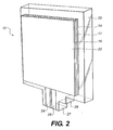
- an OLED light source 10 useful with lighting apparatus includes a substrate 20 , the substrate defining a tab portion 21 .
- An organic light emitting layer 12 is disposed between a cathode 14 and an anode 16 .
- An encapsulating cover 22 is provided over the light source 10 on the substrate 20 .
- the cover 22 may be a separate element such as a hermetically sealed cover plate affixed over the layers 12 , 14 , and 16 or the cover may be coated over the layers 12 , 14 , and 16 as an additional layer.
- the OLED light emitting layer 12 is continuous over the substrate to provide a continuous light emitting area.
- First and second conductors 24 and 26 located on the substrate 20 are electrically connected to the first and second electrodes 14 and 16 , and extend on tab portion 21 beyond the encapsulating cover 22 for making electrical contact to the first and second electrodes by an external power source (not shown).
- the tab portion 21 defines an orientation feature such as step 28 to insure that the illumination source is inserted in a lighting fixture (described below) in the correct orientation.
- the substrate 20 , the electrodes 14 and 16 , and the cover 22 are transparent. In applications where it is not required to emit light from both sides of the substrate, one or more of the substrate, cover, anode, or cathode may be opaque or reflective. The cover and/or substrate may also be light diffusers.
- a plurality of light sources 10 are held in a lighting fixture 34 .
- the lighting fixture 34 includes a plurality of apertures 36 for receiving the respective tab portions 21 of the light sources 10 and includes set of first electrical contacts 40 located in the apertures 36 for making electrical connection to the first and second conductors 24 and 26 of each of the light sources 10 .
- the lighting fixture 34 also includes second electrical contacts 38 which are electrically connected to first electrical contacts 40 for making electrical connection to an external power source (not shown).
- Duplicate first electrical contacts may be provided in the aperture 36 so that the tab portion 21 (assuming it does not include an orientation feature 28 ) may be inserted in either orientation into the aperture 36 and will still connect appropriately to the external power source.
- the light source 10 is physically inserted into or removed from the lighting fixture 34 by pushing or pulling the tab portion of the substrate into or out of the lighting fixture 34 .
- the light source 10 and the lighting fixture 34 are preferably provided with a detent (not shown) to hold the light source 10 in the fixture 34 .
- the light source 10 may be replaced by physically removing it from the fixture 34 by pulling the light source 10 out of the fixture 34 and inserting a replacement light source 10 , properly aligned, into the fixture 34 .
- the fixture 34 may be designed so that the light source cannot be inserted into the fixture backwards using techniques well known in the art. Hence, the lighting apparatus is well adapted to consumer use.
- the lighting fixture may include a power converter 42 to convert the electrical power from the external power source to a form suitable for powering the OLED light source 10 .
- the external power source is a standard power source, for example, the power supplied to a house or office at 110 V in the United States or 220 V in the United Kingdom. Other standards such as 24 V DC, 12 V DC and 6 V DC found in vehicles, for example, may also be used.
- the OLED light source 10 may require a rectified voltage with a particular waveform and magnitude; the converter 42 can provide the particular waveform using conventional power control circuitry.
- the particular waveform may periodically reverse bias the light emitting organic materials to prolong the life-time of the OLED materials in the light source 10 .
- the converter 42 is preferably located in the lighting fixture 34 , as shown in Fig. 3.
- the lighting fixture 34 may also include a switch 35 for controlling the power to the light source 10 .
- Fig. 4 illustrates an alternative embodiment of a light source useful with the present invention wherein the substrate 20 has a long thin body portion with two tabs 21 and 21' located at opposite ends of the body portion, one of the conductors 24 and 26 being located on each tab.
- a lighting fixture 34 includes a plurality of apertures 36 and 36' for receiving and holding the respective tabs of the light sources shown in Fig. 4. The light sources can be held in the fixture by detents or clips 39 in the apertures.
- the substrate 20 does not include a tab portion, and the first and second conductors are located on the edge of the substrate 20 .
- the light source 10 includes a substrate 20 with first and second conductors 24 and 26 located on the edge of the substrate 20 .
- Fig. 7 illustrates a further alternative arrangement wherein the first and second conductors 24 and 26 are located at opposite edges of the substrate 20 .
- the light source 10 may emit light from only one side (e.g. the side facing away from the lighting fixture) and the first and second conductors located on the opposite side.
- the substrate 20 can be either rigid or flexible. Rigid substrates, such as glass, provide more structural strength and may have a variety of shapes other than rectangular.
- the present invention may also be used with a flexible substrate, such as plastic, that can be bent into a variety of shapes.
- the lighting fixture 34 may include a support to hold the substrate in a desired configuration, for example, as shown in Fig. 7, a plurality of light sources 10 are curved into a cylindrical shape and supported by lighting fixture 34 . Electrical power is provided to the lighting fixture and conducted to the light sources 10 through contacts in apertures 36 in the lighting fixture 34 .
- a lighting fixture 34 includes multiple apertures 36 for a plurality of light sources 10 arranged in a row.
- the light sources each have an edge touching or nearly touching the neighboring light sources and are in a common plane.
- Multiple rows of light sources may be included in a single fixture (not shown).
- the edges not in common may form a line (as in Fig. 8) or the edges of an open polygon as in Fig. 3.
- light may be emitted and reflected from the inside of the angle or emitted from the outside.
- This concept is readily extended to a closed polygon such as is shown in Fig. 9 (with one light source omitted for clarity) wherein the light sources may emit light to the inside of the closed polygon, the outside, or both.
- Figs. 10A-D multiple rows of light sources may be aligned at an angle to each other, as shown in Figs. 10A-D.
- Light sources 10 may be provided with a reflective back surface. Light emitted from each light source 10 may be reflected from the other so as to reduce the aperture from which the light is emitted from the light sources. In this case, light sources 10 with reflective backs are preferred.
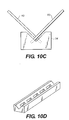
- substrates with a tab 21 of one half the width of the light source 10 can be combined in pairs (see Fig. 10B) wherein each substrate is in a different plane but sharing a common edge 62 near the tab 21 on each substrate. As shown in Fig. 10C, the pairs can be inserted at an angle into a single lighting fixture 34 .
- pairs of light sources can then be replicated along the length of a long lighting fixture 34 to provide lighting apparatus of any desired length ( see Fig. 10D) wherein the light sources conceal the lighting fixture.
- a plurality of lighting fixtures of the type shown in Figs. 10A-D can then be provided in an array to form a panel, for example in a suspended ceiling. This provides a nearly flat-panel area illuminator. The angle at which the pairs are placed controls the narrowness of the illumination aperture, the depth of the flat panel, and the width of the row.
- the fixture is hidden. Each element of each pair can be easily replaced in the fixture in the event of a failure.
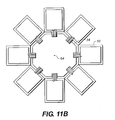
- a plurality of light emitting devices 10 are arranged in a common plane with the tabs pointing toward a common center 64 . If the light sources 10 are trapezoidal in shape, the edges can be contiguous so that the outside and inside edges of the substrates form a trapezoid and the light emitting surfaces are contiguous, as shown in Fig. 11C.
- the light sources are each slightly tilted in a common orientation, the light sources form a fan shape and may be rotated about a common point to provide a functional fan.
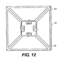
- the light sources may also be aligned so that the outside edge of each substrate forms a regular polygon in a common plane and the substrates themselves are at a common angle to the plane to form a three dimensional shape such as a polygonal cone as shown in Fig. 12. If the light sources are trapezoidal, the side edges may be joined to form an enclosing structure from one end of which the light is emitted and at the other end of which the tabs are inserted into the lighting fixture.
- Three substrates may also be arranged so that each substrate is in a different plane orthogonal to the other to form a comer cube. If the light sources have a reflective back, any light shone towards the comer cube may be reflected back whence the light came.
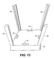
- lighting fixtures in which the edges of the light sources are touching in a common line (or nearly touching) can include decorative channels 48 similar to stained glass caming to improve their aesthetic appearance, to hold the substrates in alignment.
- the light sources useful in the present invention may also be provided with decorative substrates or encapsulating covers may be painted or composed of colored material to provide a stained glass look.
- patterns may be cut or etched into the surfaces of the substrate and/or cover to provide pleasing patterns, graphic elements such as logos or pictures, or light refractive properties.
- the OLED layer comprises Organic Light Emitting Diodes (OLEDs) which are composed of small molecule OLEDs as disclosed in but not limited to US Patent 4,769,292, issued September 6, 1988 to Tang et al., and US Patent 5,061,569, issued October 29, 1991 to VanSlyke et al.
- OLEDs Organic Light Emitting Diodes
- a typical, non-limiting structure is shown in Fig. 14 and is comprised of an anode layer 103 , a hole-injecting layer 105 , a hole-transporting layer 107 , a light-emitting layer 109 , an electron-transporting layer 111 , and a cathode layer 113 . These layers are described in detail below.
- the total combined thickness of the organic layers is preferably less than 500 nm.
- a voltage/current source 250 is required to energize the OLED element and conductive wiring 260 is required to make electrical contact to the anode and cathode.
- Substrate 20 is preferably light transmissive but may also be opaque or reflective.
- Substrates for use in this case include, but are not limited to, glass, plastic, semiconductor materials, ceramics, and circuit board materials.
- the anode layer 103 is preferably transparent or substantially transparent to the light emitted by the OLED layer(s).
- Common transparent anode materials used in this invention are indium-tin oxide (ITO), indium-zinc oxide (IZO) and tin oxide, but other metal oxides can work including, but not limited to, aluminum- or indium-doped zinc oxide, magnesium-indium oxide, and nickel-tungsten oxide.
- metal nitrides such as gallium nitride
- metal selenides such as zinc selenide
- metal sulfides such as zinc sulfide
- the light transmitting characteristics of layer 103 are immaterial and any conductive material can be used, transparent, opaque or reflective.
- Example conductors for this application include, but are not limited to, gold, iridium, molybdenum, palladium, and platinum.
- Typical anode materials, transmissive or otherwise, have a work function of 4.1 eV or greater. Desired anode materials are commonly deposited by any suitable means such as evaporation, sputtering, chemical vapor deposition, or electrochemical means.
- Anodes can be patterned using well-known photolithographic processes.
- a hole-injecting layer 105 be provided between anode 103 and hole-transporting layer 107 .
- the hole-injecting material can serve to improve the film formation property of subsequent organic layers and to facilitate injection of holes into the hole-transporting layer.
- Suitable materials for use in the hole-injecting layer include, but are not limited to, porphyrinic compounds as described in US 4,720,432, and plasma-deposited fluorocarbon polymers as described in US 6,208,075.
- Alternative hole-injecting materials reportedly useful in organic EL devices are described in EP 0 891 121 A1 and EP 1029 909 A1.
- the hole-transporting layer 107 contains at least one hole-transporting compound such as an aromatic tertiary amine, where the latter is understood to be a compound containing at least one trivalent nitrogen atom that is bonded only to carbon atoms, at least one of which is a member of an aromatic ring.
- the aromatic tertiary amine can be an arylamine, such as a monoarylamine, diarylamine, triarylamine, or a polymeric arylamine. Exemplary monomeric triarylamines are illustrated by Klupfel et al. US 3,180,730.
- aromatic tertiary amines substituted with one or more vinyl radicals and/or comprising at least one active hydrogen containing group are disclosed by Brantley et al US 3,567,450 and US 3,658,520.
- a more preferred class of aromatic tertiary amines are those which include at least two aromatic tertiary amine moieties as described in US 4,720,432 and US 5,061,569.
- Illustrative of useful aromatic tertiary amines include, but are not limited to, the following:
- Another class of useful hole-transporting materials includes polycyclic aromatic compounds as described in EP 1 009 041.
- polymeric hole-transporting materials can be used such as poly(N-vinylcarbazole) (PVK), polythiophenes, polypyrrole, polyaniline, and copolymers such as poly(3,4-ethylenedioxythiophene) / poly(4-styrenesulfonate) also called PEDOT/PSS.
- the light-emitting layer (LEL) 109 of the organic EL element comprises a luminescent or fluorescent material where electroluminescence is produced as a result of electron-hole pair recombination in this region.
- the light-emitting layer can be comprised of a single material, but more commonly consists of a host material doped with a guest compound or compounds where light emission comes primarily from the dopant and can be of any color.
- the host materials in the light-emitting layer can be an electron-transporting material, as defined below, a hole-transporting material, as defined above, or another material or combination of materials that support hole-electron recombination.
- the dopant is usually chosen from highly fluorescent dyes, but phosphorescent compounds, e.g., transition metal complexes as described in WO 98/55561, WO 00/18851, WO 00/57676, and WO 00/70655 are also useful. Dopants are typically coated as 0.01 to 10 % by weight into the host material. Iridium complexes of phenylpyridine and its derivatives are particularly useful luminescent dopants. Polymeric materials such as polyfluorenes and polyvinylarylenes (e.g., poly(p-phenylenevinylene), PPV) can also be used as the host material. In this case, small molecule dopants can be molecularly dispersed into the polymeric host, or the dopant could be added by copolymerizing a minor constituent into the host polymer.
- phosphorescent compounds e.g., transition metal complexes as described in WO 98/55561, WO 00/18851, WO 00
- Host and emitting molecules known to be of use include, but are not limited to, those disclosed in US 4,769,292, US 5,141,671, US 5,150,006, US 5,151,629, US 5,405,709, US 5,484,922, US 5,593,788, US 5,645,948, US 5,683,823, US 5,755,999, US 5,928,802, US 5,935,720, US 5,935,721, and US 6,020,078.
- Metal complexes of 8-hydroxyquinoline and similar oxine derivatives constitute one class of useful host compounds capable of supporting electroluminescence, and are particularly suitable.
- useful chelated oxinoid compounds are the following:
- useful host materials include, but are not limited to: derivatives of anthracene, such as 9,10-di-(2-naphthyl)anthracene and derivatives thereof, distyrylarylene derivatives as described in US 5,121,029, and benzazole derivatives, for example, 2,2',2"-(1,3,5-phenylene)tris[1-phenyl-1H-benzimidazole].
- Useful fluorescent dopants include, but are not limited to, derivatives of anthracene, tetracene, xanthene, perylene, rubrene, coumarin, rhodamine, quinacridone, dicyanomethylenepyran compounds, thiopyran compounds, polymethine compounds, pyrilium and thiapyrilium compounds, fluorene derivatives, periflanthene derivatives and carbostyryl compounds.
- Preferred thin film-forming materials for use in forming the electron-transporting layer 111 of the organic EL elements of this invention are metal chelated oxinoid compounds, including chelates of oxine itself (also commonly referred to as 8-quinolinol or 8-hydroxyquinoline). Such compounds help to inject and transport electrons, exhibit high levels of performance, and are readily fabricated in the form of thin films. Exemplary oxinoid compounds were listed previously.
- electron-transporting materials include various butadiene derivatives as disclosed in US 4,356,429 and various heterocyclic optical brighteners as described in US 4,539,507. Benzazoles and triazines are also useful electron-transporting materials.
- layers 111 and 109 can optionally be collapsed into a single layer that serves the function of supporting both light emission and electron transport. These layers can be collapsed in both small molecule OLED systems and in polymeric OLED systems.
- a hole-transporting layer such as PEDOT-PSS with a polymeric light-emitting layer such as PPV.
- PPV serves the function of supporting both light emission and electron transport.
- the cathode 113 is transparent and can comprise nearly any conductive transparent material.
- the cathode 113 may be opaque or reflective.
- Suitable cathode materials have good film-forming properties to ensure good contact with the underlying organic layer, promote electron injection at low voltage, and have good stability.
- Useful cathode materials often contain a low work function metal ( ⁇ 4.0 eV) or metal alloy.
- One preferred cathode material is comprised of a Mg:Ag alloy wherein the percentage of silver is in the range of 1 to 20 %, as described in US Patent 4,885,221.
- Another suitable class of cathode materials includes bilayers comprising a thin electron-injection layer (EIL) and a thicker layer of conductive metal.
- the EIL is situated between the cathode and the organic layer (e.g., ETL).
- the EIL preferably includes a low work function metal or metal salt, and if so, the thicker conductor layer does not need to have a low work function.
- One such cathode is comprised of a thin layer of LiF followed by a thicker layer of A1 as described in US 5,677,572.
- Other useful cathode material sets include, but are not limited to, those disclosed in US 5,059,861, 5,059,862, and 6,140,763.
- cathode layer 113 When cathode layer 113 is transparent or nearly transparent, metals must be thin or transparent conductive oxides, or a combination of these materials.
- Optically transparent cathodes have been described in more detail in US 4,885,211, US 5,247,190, JP 3,234,963, US 5,703,436, US 5,608,287, US 5,837,391, US 5,677,572, US 5,776,622, US 5,776,623, US 5,714,838, US 5,969,474, US 5,739,545, US 5,981,306, US 6,137,223, US 6,140,763, US 6,172,459, EP 1 076 368, and US 6,278,236.
- Cathode materials are typically deposited by evaporation, sputtering, or chemical vapor deposition. When needed, patterning can be achieved through many well known methods including, but not limited to, through-mask deposition, integral shadow masking as described in US 5,276,380 and EP 0 732 868, laser ablation, and selective chemical vapor deposition.
- the organic materials mentioned above are suitably deposited through a vapor-phase method such as sublimation, but can be deposited from a fluid, for example, from a solvent with an optional binder to improve film formation. If the material is a polymer, solvent deposition is useful but other methods can be used, such as sputtering or thermal transfer from a donor sheet.
- the material to be deposited by sublimation can be vaporized from a sublimator "boat" often comprised of a tantalum material, e.g., as described in US 6,237,529, or can be first coated onto a donor sheet and then sublimed in closer proximity to the substrate.
- Layers with a mixture of materials can utilize separate sublimator boats or the materials can be pre-mixed and coated from a single boat or donor sheet. Deposition can also be achieved using thermal dye transfer from a donor sheet (see US 5,851,709 and 6,066,357) and inkjet method (see US 6,066,357).
- OLED devices of this invention can employ various well-known optical effects in order to enhance its properties if desired. This includes optimizing layer thicknesses to yield maximum light transmission, providing dielectric mirror structures, replacing reflective electrodes with light-absorbing electrodes, or providing colored, neutral density, or color conversion filters over the device. Filters, may be specifically provided over the cover or substrate or as part of the cover or substrate.
Landscapes
- Engineering & Computer Science (AREA)
- General Engineering & Computer Science (AREA)
- Electroluminescent Light Sources (AREA)
- Arrangement Of Elements, Cooling, Sealing, Or The Like Of Lighting Devices (AREA)
- Planar Illumination Modules (AREA)
- Illuminated Signs And Luminous Advertising (AREA)
Abstract
Description
- The present invention relates to the use of organic light emitting diode devices for area illumination.
- Solid-state lighting devices made of light emitting diodes are increasingly useful for applications requiring robustness and long-life. For example, solid-state LEDs are found today in automotive applications. These devices are typically formed by combining multiple, small LED devices providing a point light source into a single module together with glass lenses suitably designed to control the light as is desired for a particular application (see, for example WO99/57945, published November 11, 1999). These multiple devices are expensive and complex to manufacture and integrate into single area illumination devices. Moreover, LED devices provide point sources of light, a plurality of which are employed for area illumination.
- Organic light emitting diodes (OLEDs) are manufactured by depositing organic semiconductor materials between electrodes on a substrate. This process enables the creation of light sources having extended surface area on a single substrate. The prior art describes the use of electro-luminescent materials as adjuncts to conventional lighting (for example US 6,168,282 issued January 2, 2001 to Chien). In this case, because of the limited light output from the electro-luminescent material, it is not useful for primary lighting.
- EP1120838A2, published August 1, 2001, describes a method for mounting multiple organic light emitting devices on a mounting substrate to create a light source. However, this approach of mounting multiple light sources on a substrate increases the complexity and hence the manufacturing costs of the area illumination light source. Moreover, in this design the multiple substrates are not readily replaced by consumers if they should fail. In addition, each lighting device must be readily and safely replaced by consumers at minimal cost.
- There is a need therefore for an improved, replaceable OLED area illumination device having a simple construction using a single substrate and compatibility with the existing lighting infrastructure.
- The need is met according to the present invention by providing a solid-state area illumination lighting apparatus that includes a plurality of light sources, each light source having, a substrate; an organic light emitting diode (OLED) layer deposited upon the substrate, the organic light emitting diode layer including first and second electrodes for providing electrical power to the OLED layer; an encapsulating cover covering the OLED layer; and first and second conductors located on the substrate and electrically connected to the first and second electrodes, and extending beyond the encapsulating cover for making electrical contact to the first and second electrodes by an external power source; and a lighting fixture for removably receiving and holding the plurality of light sources and having a plurality of first electrical contacts for making electrical connection to the first and second conductors of the light sources, and second electrical contacts for making electrical connection to an external power source.
- The present invention has the advantage of providing a fixture together with inexpensive, long-lived, highly efficient light sources that are replaceable, and are compatible with the existing lighting infrastructure and requirements.
- Fig. 1 illustrates a cross sectional view of a prior art conventional OLED illumination device;
- Fig. 2 is a perspective view of a light source useful with the present invention;
- Fig. 3 is a perspective view of a lighting apparatus according to one embodiment of the present invention;
- Fig. 4 is a perspective view of an alternative light source useful with the present invention;
- Fig. 5 is a top view of a lighting fixture used with the light source shown in Fig. 4 according to an alternative embodiment of the present invention;
- Fig. 6 is a perspective view of an alternative light source useful with the present invention;
- Fig. 7 is a perspective view of an alternative light source useful with the present invention;
- Fig. 8 is a perspective view of a lighting apparatus according to a further alternative embodiment of the present invention;
- Fig. 9 is a perspective view of lighting apparatus according to a further alternative embodiment of the present invention;
- Fig. 10A-D are perspective views of a lighting apparatus according to a further alternative embodiment of the present invention;
- Fig. 11 A-C are plan views of a lighting apparatus having light sources arranged in a variety of fan shaped configurations according to one embodiment of the present invention;
- Fig. 12 is a plan view of a lighting apparatus having light sources arranged in a pyramidal arrangement;
- Fig. 13 is a perspective view of a lighting fixture having decorative channels for receiving the edges of light sources according to one embodiment of the present invention; and
- Fig. 14 is a cross sectional view of an OLED light source as known in the prior art.
-
- It will be understood that the figures are not to scale since the individual layers are too thin and the thickness differences of various layers too great to permit depiction to scale.
- It is difficult to manufacture large, flat-panel area illumination devices. Large substrates require manufacturing facilities capable of handling large substrates and increase the likelihood of failure due to handling, use, or environment effects. In contrast, the use of smaller, multiple replaceable elements within a single fixture requires less expensive materials, simpler manufacturing processes, and is more robust in the presence of failure, since a single element failure does not cause an entire area illumination device to fail and a single element may be replaced at lower cost. Moreover, multiple, smaller elements are more readily transported. However, this design approach does require the use of fixtures capable of properly aligning, accessing, and providing power to multiple display elements.
- Fig. 1 is a schematic diagram of a prior art OLED light source including an organic
light emitting layer 12 disposed between two electrodes, e.g. acathode 14 and ananode 16. The organiclight emitting layer 12 emits light upon application of a voltage from apower source 18 across the electrodes. The OLEDlight source 10 typically includes asubstrate 20 such as glass or plastic. It will be understood that the relative locations of theanode 16 andcathode 14 may be reversed with respect to the substrate. The term OLED light source refers to the combination of the organiclight emitting layer 12, thecathode 14, theanode 16, and other layers described below. - Referring to Fig. 2, an
OLED light source 10 useful with lighting apparatus according to the present invention includes asubstrate 20, the substrate defining atab portion 21. An organiclight emitting layer 12 is disposed between acathode 14 and ananode 16. Anencapsulating cover 22 is provided over thelight source 10 on thesubstrate 20. - The
cover 22 may be a separate element such as a hermetically sealed cover plate affixed over thelayers layers light emitting layer 12 is continuous over the substrate to provide a continuous light emitting area. First andsecond conductors substrate 20 are electrically connected to the first andsecond electrodes tab portion 21 beyond theencapsulating cover 22 for making electrical contact to the first and second electrodes by an external power source (not shown). - In a preferred embodiment of the present invention, the
tab portion 21 defines an orientation feature such asstep 28 to insure that the illumination source is inserted in a lighting fixture (described below) in the correct orientation. To allow light to be emitted from theOLED light source 10, thesubstrate 20, theelectrodes cover 22 are transparent. In applications where it is not required to emit light from both sides of the substrate, one or more of the substrate, cover, anode, or cathode may be opaque or reflective. The cover and/or substrate may also be light diffusers. - Referring to Fig. 3, according to the present invention, a plurality of
light sources 10 are held in alighting fixture 34. Thelighting fixture 34 includes a plurality ofapertures 36 for receiving therespective tab portions 21 of thelight sources 10 and includes set of firstelectrical contacts 40 located in theapertures 36 for making electrical connection to the first andsecond conductors light sources 10. Thelighting fixture 34 also includes secondelectrical contacts 38 which are electrically connected to firstelectrical contacts 40 for making electrical connection to an external power source (not shown). - Duplicate first electrical contacts may be provided in the
aperture 36 so that the tab portion 21 (assuming it does not include an orientation feature 28) may be inserted in either orientation into theaperture 36 and will still connect appropriately to the external power source. Thelight source 10 is physically inserted into or removed from thelighting fixture 34 by pushing or pulling the tab portion of the substrate into or out of thelighting fixture 34. Thelight source 10 and thelighting fixture 34 are preferably provided with a detent (not shown) to hold thelight source 10 in thefixture 34. - The
light source 10 may be replaced by physically removing it from thefixture 34 by pulling thelight source 10 out of thefixture 34 and inserting areplacement light source 10, properly aligned, into thefixture 34. Thefixture 34 may be designed so that the light source cannot be inserted into the fixture backwards using techniques well known in the art. Hence, the lighting apparatus is well adapted to consumer use. - The lighting fixture may include a
power converter 42 to convert the electrical power from the external power source to a form suitable for powering theOLED light source 10. In a preferred embodiment, the external power source is a standard power source, for example, the power supplied to a house or office at 110 V in the United States or 220 V in the United Kingdom. Other standards such as 24 V DC, 12 V DC and 6 V DC found in vehicles, for example, may also be used. - The OLED
light source 10 may require a rectified voltage with a particular waveform and magnitude; theconverter 42 can provide the particular waveform using conventional power control circuitry. The particular waveform may periodically reverse bias the light emitting organic materials to prolong the life-time of the OLED materials in thelight source 10. Theconverter 42 is preferably located in thelighting fixture 34, as shown in Fig. 3. Thelighting fixture 34 may also include aswitch 35 for controlling the power to thelight source 10. - Fig. 4 illustrates an alternative embodiment of a light source useful with the present invention wherein the
substrate 20 has a long thin body portion with twotabs 21 and 21' located at opposite ends of the body portion, one of theconductors lighting fixture 34 includes a plurality ofapertures 36 and 36' for receiving and holding the respective tabs of the light sources shown in Fig. 4. The light sources can be held in the fixture by detents orclips 39 in the apertures. - Referring to Fig. 6, in a further alternative embodiment of the
light source 10 useful in the lighting apparatus of the present invention, thesubstrate 20 does not include a tab portion, and the first and second conductors are located on the edge of thesubstrate 20. Thelight source 10 includes asubstrate 20 with first andsecond conductors substrate 20. Fig. 7 illustrates a further alternative arrangement wherein the first andsecond conductors substrate 20. Thelight source 10 may emit light from only one side (e.g. the side facing away from the lighting fixture) and the first and second conductors located on the opposite side. - The
substrate 20 can be either rigid or flexible. Rigid substrates, such as glass, provide more structural strength and may have a variety of shapes other than rectangular. The present invention may also be used with a flexible substrate, such as plastic, that can be bent into a variety of shapes. In the case wherein the substrate is flexible, thelighting fixture 34 may include a support to hold the substrate in a desired configuration, for example, as shown in Fig. 7, a plurality oflight sources 10 are curved into a cylindrical shape and supported bylighting fixture 34. Electrical power is provided to the lighting fixture and conducted to thelight sources 10 through contacts inapertures 36 in thelighting fixture 34. - A great variety of decorative and special-purpose effects are readily created by the use of multiple light sources in a single lighting fixture. Directional lighting is readily achieved by providing rectangular substrates mounted so that the substrates have an edge in common (touching, or nearly touching). Referring to Fig. 8, a
lighting fixture 34 includesmultiple apertures 36 for a plurality oflight sources 10 arranged in a row. The light sources each have an edge touching or nearly touching the neighboring light sources and are in a common plane. Multiple rows of light sources may be included in a single fixture (not shown). The edges not in common may form a line (as in Fig. 8) or the edges of an open polygon as in Fig. 3. In the lighting apparatus of Fig. 3, light may be emitted and reflected from the inside of the angle or emitted from the outside. This concept is readily extended to a closed polygon such as is shown in Fig. 9 (with one light source omitted for clarity) wherein the light sources may emit light to the inside of the closed polygon, the outside, or both. - Alternatively, multiple rows of light sources may be aligned at an angle to each other, as shown in Figs. 10A-D. Light sources 10 may be provided with a reflective back surface. Light emitted from each
light source 10 may be reflected from the other so as to reduce the aperture from which the light is emitted from the light sources. In this case,light sources 10 with reflective backs are preferred. Referring to Fig. 10A, substrates with atab 21 of one half the width of thelight source 10 can be combined in pairs (see Fig. 10B) wherein each substrate is in a different plane but sharing acommon edge 62 near thetab 21 on each substrate. As shown in Fig. 10C, the pairs can be inserted at an angle into asingle lighting fixture 34. These pairs of light sources can then be replicated along the length of along lighting fixture 34 to provide lighting apparatus of any desired length ( see Fig. 10D) wherein the light sources conceal the lighting fixture. A plurality of lighting fixtures of the type shown in Figs. 10A-D can then be provided in an array to form a panel, for example in a suspended ceiling. This provides a nearly flat-panel area illuminator. The angle at which the pairs are placed controls the narrowness of the illumination aperture, the depth of the flat panel, and the width of the row. By inter-digitating the light sources, the fixture is hidden. Each element of each pair can be easily replaced in the fixture in the event of a failure. By connecting the light sources in parallel with the others, a robust, gracefully degrading lighting fixture is created. - Referring to Figs. 11 A, B and C, in an alternative embodiment, a plurality of light emitting
devices 10 are arranged in a common plane with the tabs pointing toward acommon center 64. If thelight sources 10 are trapezoidal in shape, the edges can be contiguous so that the outside and inside edges of the substrates form a trapezoid and the light emitting surfaces are contiguous, as shown in Fig. 11C. - If the light sources are each slightly tilted in a common orientation, the light sources form a fan shape and may be rotated about a common point to provide a functional fan.
- The light sources may also be aligned so that the outside edge of each substrate forms a regular polygon in a common plane and the substrates themselves are at a common angle to the plane to form a three dimensional shape such as a polygonal cone as shown in Fig. 12. If the light sources are trapezoidal, the side edges may be joined to form an enclosing structure from one end of which the light is emitted and at the other end of which the tabs are inserted into the lighting fixture.
- Three substrates may also be arranged so that each substrate is in a different plane orthogonal to the other to form a comer cube. If the light sources have a reflective back, any light shone towards the comer cube may be reflected back whence the light came.
- Referring to Fig. 13, lighting fixtures in which the edges of the light sources are touching in a common line (or nearly touching) can include
decorative channels 48 similar to stained glass caming to improve their aesthetic appearance, to hold the substrates in alignment. The light sources useful in the present invention may also be provided with decorative substrates or encapsulating covers may be painted or composed of colored material to provide a stained glass look. Alternatively, patterns may be cut or etched into the surfaces of the substrate and/or cover to provide pleasing patterns, graphic elements such as logos or pictures, or light refractive properties. - In a preferred embodiment, the OLED layer comprises Organic Light Emitting Diodes (OLEDs) which are composed of small molecule OLEDs as disclosed in but not limited to US Patent 4,769,292, issued September 6, 1988 to Tang et al., and US Patent 5,061,569, issued October 29, 1991 to VanSlyke et al.
- Further details with regard to OLED materials and construction are described below.
- There are numerous configurations of OLED elements wherein the present invention can be successfully practiced. A typical, non-limiting structure is shown in Fig. 14 and is comprised of an
anode layer 103, a hole-injectinglayer 105, a hole-transportinglayer 107, a light-emittinglayer 109, an electron-transportinglayer 111, and acathode layer 113. These layers are described in detail below. The total combined thickness of the organic layers is preferably less than 500 nm. A voltage/current source 250 is required to energize the OLED element andconductive wiring 260 is required to make electrical contact to the anode and cathode. -
Substrate 20 is preferably light transmissive but may also be opaque or reflective. Substrates for use in this case include, but are not limited to, glass, plastic, semiconductor materials, ceramics, and circuit board materials. - The
anode layer 103 is preferably transparent or substantially transparent to the light emitted by the OLED layer(s). Common transparent anode materials used in this invention are indium-tin oxide (ITO), indium-zinc oxide (IZO) and tin oxide, but other metal oxides can work including, but not limited to, aluminum- or indium-doped zinc oxide, magnesium-indium oxide, and nickel-tungsten oxide. In addition to these oxides, metal nitrides, such as gallium nitride, and metal selenides, such as zinc selenide, and metal sulfides, such as zinc sulfide, can be used inlayer 103. When the anode is not transparent, the light transmitting characteristics oflayer 103 are immaterial and any conductive material can be used, transparent, opaque or reflective. Example conductors for this application include, but are not limited to, gold, iridium, molybdenum, palladium, and platinum. Typical anode materials, transmissive or otherwise, have a work function of 4.1 eV or greater. Desired anode materials are commonly deposited by any suitable means such as evaporation, sputtering, chemical vapor deposition, or electrochemical means. Anodes can be patterned using well-known photolithographic processes. - It is often useful that a hole-injecting
layer 105 be provided betweenanode 103 and hole-transportinglayer 107. The hole-injecting material can serve to improve the film formation property of subsequent organic layers and to facilitate injection of holes into the hole-transporting layer. Suitable materials for use in the hole-injecting layer include, but are not limited to, porphyrinic compounds as described in US 4,720,432, and plasma-deposited fluorocarbon polymers as described in US 6,208,075. Alternative hole-injecting materials reportedly useful in organic EL devices are described in EP 0 891 121 A1 and EP 1029 909 A1. - The hole-transporting
layer 107 contains at least one hole-transporting compound such as an aromatic tertiary amine, where the latter is understood to be a compound containing at least one trivalent nitrogen atom that is bonded only to carbon atoms, at least one of which is a member of an aromatic ring. In one form the aromatic tertiary amine can be an arylamine, such as a monoarylamine, diarylamine, triarylamine, or a polymeric arylamine. Exemplary monomeric triarylamines are illustrated by Klupfel et al. US 3,180,730. Other suitable triarylamines substituted with one or more vinyl radicals and/or comprising at least one active hydrogen containing group are disclosed by Brantley et al US 3,567,450 and US 3,658,520. A more preferred class of aromatic tertiary amines are those which include at least two aromatic tertiary amine moieties as described in US 4,720,432 and US 5,061,569. Illustrative of useful aromatic tertiary amines include, but are not limited to, the following: - 1,1-Bis(4-di- p -tolylaminophenyl)cyclohexane
- 1,1 -Bis(4-di- p -tolylaminophenyl)-4-phenylcyclohexane
- 4,4'-Bis(diphenylamino)quadriphenyl
- Bis(4-dimethylamino-2-methylphenyl)-phenylmethane
- N,N,N-Tri( p -tolyl)amine
- 4-(di-p-tolylamino)-4'-[4(di- p -tolylamino)-styryl]stilbene
- N,N,N',N'-Tetra- p -tolyl-4-4'-diaminobiphenyl
- N,N,N',N'-Tetraphenyl-4,4'-diaminobiphenyl
- N,N,N',N'-tetra-1-naphthyl-4,4'-diaminobiphenyl
- N,N,N',N'-tetra-2-naphthyl-4,4'-diaminobiphenyl
- N-Phenylcarbazole
- 4,4'-Bis[N-(1-naphthyl)-N-phenylamino]biphenyl
- 4,4'-Bis[N-(1-naphthyl)-N-(2-naphthyl)amino]biphenyl
- 4,4"-Bis[N-(1-naphthyl)-N-phenylamino]p-terphenyl
- 4,4'-Bis[N-(2-naphthyl)-N-phenylamino]biphenyl
- 4,4'-Bis[N-(3-acenaphthenyl)-N-phenylamino]biphenyl
- 1,5-Bis[N-(1-naphthyl)-N-phenylamino]naphthalene
- 4,4'-Bis[N-(9-anthryl)-N-phenylamino]biphenyl
- 4,4"-Bis[N-(1-anthryl)-N-phenylamino]- p -terphenyl
- 4,4'-Bis[N-(2-phenanthryl)-N-phenylamino]biphenyl
- 4,4'-Bis[N-(8-fluoranthenyl)-N-phenylamino]biphenyl
- 4,4'-Bis[N-(2-pyrenyl)-N-phenylamino]biphenyl
- 4,4'-Bis[N-(2-naphthacenyl)-N-phenylamino]biphenyl
- 4,4'-Bis[N-(2-perylenyl)-N-phenylamino]biphenyl
- 4,4'-Bis[N-(1-coronenyl)-N-phenylamino]biphenyl
- 2,6-Bis(di- p -tolylamino)naphthalene
- 2,6-Bis[di-(1-naphthyl)amino]naphthalene
- 2,6-Bis[N-(1-naphthyl)-N-(2-naphthyl)amino]naphthalene
- N,N,N',N'-Tetra(2-naphthyl)-4,4"-diamino- p -terphenyl
- 4,4'-Bis {N-phenyl-N-[4-(1naphthyl)-phenyl]amino}biphenyl
- 4,4'-Bis[N-phenyl-N-(2-pyrenyl)amino]biphenyl
- 2,6-Bis[N,N-di(2-naphthyl)amine]fluorene
- 1,5-Bis[N-(1-naphthyl)-N-phenylamino]naphthalene
-
- Another class of useful hole-transporting materials includes polycyclic aromatic compounds as described in EP 1 009 041. In addition, polymeric hole-transporting materials can be used such as poly(N-vinylcarbazole) (PVK), polythiophenes, polypyrrole, polyaniline, and copolymers such as poly(3,4-ethylenedioxythiophene) / poly(4-styrenesulfonate) also called PEDOT/PSS.
- As more fully described in US 4,769,292 and 5,935,721, the light-emitting layer (LEL) 109 of the organic EL element comprises a luminescent or fluorescent material where electroluminescence is produced as a result of electron-hole pair recombination in this region. The light-emitting layer can be comprised of a single material, but more commonly consists of a host material doped with a guest compound or compounds where light emission comes primarily from the dopant and can be of any color. The host materials in the light-emitting layer can be an electron-transporting material, as defined below, a hole-transporting material, as defined above, or another material or combination of materials that support hole-electron recombination. The dopant is usually chosen from highly fluorescent dyes, but phosphorescent compounds, e.g., transition metal complexes as described in WO 98/55561, WO 00/18851, WO 00/57676, and WO 00/70655 are also useful. Dopants are typically coated as 0.01 to 10 % by weight into the host material. Iridium complexes of phenylpyridine and its derivatives are particularly useful luminescent dopants. Polymeric materials such as polyfluorenes and polyvinylarylenes (e.g., poly(p-phenylenevinylene), PPV) can also be used as the host material. In this case, small molecule dopants can be molecularly dispersed into the polymeric host, or the dopant could be added by copolymerizing a minor constituent into the host polymer.
- An important relationship for choosing a dye as a dopant is a comparison of the bandgap potential which is defined as the energy difference between the highest occupied molecular orbital and the lowest unoccupied molecular orbital of the molecule. For efficient energy transfer from the host to the dopant molecule, a necessary condition is that the band gap of the dopant is smaller than that of the host material.
- Host and emitting molecules known to be of use include, but are not limited to, those disclosed in US 4,769,292, US 5,141,671, US 5,150,006, US 5,151,629, US 5,405,709, US 5,484,922, US 5,593,788, US 5,645,948, US 5,683,823, US 5,755,999, US 5,928,802, US 5,935,720, US 5,935,721, and US 6,020,078.
- Metal complexes of 8-hydroxyquinoline and similar oxine derivatives constitute one class of useful host compounds capable of supporting electroluminescence, and are particularly suitable. Illustrative of useful chelated oxinoid compounds are the following:
- CO-1:
- Aluminum trisoxine [alias, tris(8-quinolinolato)aluminum(III)]
- CO-2:
- Magnesium bisoxine [alias, bis(8-quinolinolato)magnesium(II)]
- CO-3:
- Bis[benzo{f}-8-quinolinolato]zinc (II)
- CO-4:
- Bis(2-methyl-8-quinolinolato)aluminum(III)-µ-oxo-bis(2-methyl-8-quinolinolato) aluminum(III)
- CO-5:
- Indium trisoxine [alias, tris(8-quinolinolato)indium]
- CO-6:
- Aluminum tris(5-methyloxine) [alias, tris(5-methyl-8-quinolinolato) aluminum(III)]
- CO-7:
- Lithium oxine [alias, (8-quinolinolato)lithium(I)]
- CO-8:
- Gallium oxine [alias, tris(8-quinolinolato)gallium(III)]
- CO-9:
- Zirconium oxine [alias, tetra(8-quinolinolato)zirconium(IV)]
- Other classes of useful host materials include, but are not limited to: derivatives of anthracene, such as 9,10-di-(2-naphthyl)anthracene and derivatives thereof, distyrylarylene derivatives as described in US 5,121,029, and benzazole derivatives, for example, 2,2',2"-(1,3,5-phenylene)tris[1-phenyl-1H-benzimidazole].
- Useful fluorescent dopants include, but are not limited to, derivatives of anthracene, tetracene, xanthene, perylene, rubrene, coumarin, rhodamine, quinacridone, dicyanomethylenepyran compounds, thiopyran compounds, polymethine compounds, pyrilium and thiapyrilium compounds, fluorene derivatives, periflanthene derivatives and carbostyryl compounds.
- Preferred thin film-forming materials for use in forming the electron-transporting
layer 111 of the organic EL elements of this invention are metal chelated oxinoid compounds, including chelates of oxine itself (also commonly referred to as 8-quinolinol or 8-hydroxyquinoline). Such compounds help to inject and transport electrons, exhibit high levels of performance, and are readily fabricated in the form of thin films. Exemplary oxinoid compounds were listed previously. - Other electron-transporting materials include various butadiene derivatives as disclosed in US 4,356,429 and various heterocyclic optical brighteners as described in US 4,539,507. Benzazoles and triazines are also useful electron-transporting materials.
- In some instances,
layers - Preferably, the
cathode 113 is transparent and can comprise nearly any conductive transparent material. Alternatively, thecathode 113 may be opaque or reflective. Suitable cathode materials have good film-forming properties to ensure good contact with the underlying organic layer, promote electron injection at low voltage, and have good stability. Useful cathode materials often contain a low work function metal (< 4.0 eV) or metal alloy. One preferred cathode material is comprised of a Mg:Ag alloy wherein the percentage of silver is in the range of 1 to 20 %, as described in US Patent 4,885,221. Another suitable class of cathode materials includes bilayers comprising a thin electron-injection layer (EIL) and a thicker layer of conductive metal. The EIL is situated between the cathode and the organic layer (e.g., ETL). Here, the EIL preferably includes a low work function metal or metal salt, and if so, the thicker conductor layer does not need to have a low work function. One such cathode is comprised of a thin layer of LiF followed by a thicker layer of A1 as described in US 5,677,572. Other useful cathode material sets include, but are not limited to, those disclosed in US 5,059,861, 5,059,862, and 6,140,763. - When
cathode layer 113 is transparent or nearly transparent, metals must be thin or transparent conductive oxides, or a combination of these materials. Optically transparent cathodes have been described in more detail in US 4,885,211, US 5,247,190, JP 3,234,963, US 5,703,436, US 5,608,287, US 5,837,391, US 5,677,572, US 5,776,622, US 5,776,623, US 5,714,838, US 5,969,474, US 5,739,545, US 5,981,306, US 6,137,223, US 6,140,763, US 6,172,459, EP 1 076 368, and US 6,278,236. Cathode materials are typically deposited by evaporation, sputtering, or chemical vapor deposition. When needed, patterning can be achieved through many well known methods including, but not limited to, through-mask deposition, integral shadow masking as described in US 5,276,380 and EP 0 732 868, laser ablation, and selective chemical vapor deposition. - The organic materials mentioned above are suitably deposited through a vapor-phase method such as sublimation, but can be deposited from a fluid, for example, from a solvent with an optional binder to improve film formation. If the material is a polymer, solvent deposition is useful but other methods can be used, such as sputtering or thermal transfer from a donor sheet. The material to be deposited by sublimation can be vaporized from a sublimator "boat" often comprised of a tantalum material, e.g., as described in US 6,237,529, or can be first coated onto a donor sheet and then sublimed in closer proximity to the substrate. Layers with a mixture of materials can utilize separate sublimator boats or the materials can be pre-mixed and coated from a single boat or donor sheet. Deposition can also be achieved using thermal dye transfer from a donor sheet (see US 5,851,709 and 6,066,357) and inkjet method (see US 6,066,357).
- OLED devices of this invention can employ various well-known optical effects in order to enhance its properties if desired. This includes optimizing layer thicknesses to yield maximum light transmission, providing dielectric mirror structures, replacing reflective electrodes with light-absorbing electrodes, or providing colored, neutral density, or color conversion filters over the device. Filters, may be specifically provided over the cover or substrate or as part of the cover or substrate.
Claims (2)
- A solid-state area illumination lighting apparatus, comprising:a) a plurality of light sources, each light source having,i) a substrate;ii) an organic light emitting diode (OLED) layer deposited upon the substrate, the organic light emitting diode layer including first and second electrodes for providing electrical power to the OLED layer;iii) an encapsulating cover covering the OLED layer; andiv) first and second conductors located on the substrate and electrically connected to the first and second electrodes, and extending beyond the encapsulating cover for making electrical contact to the first and second electrodes by an external power source; andb) a lighting fixture for removably receiving and holding the plurality of light sources and having a plurality of first electrical contacts for making electrical connection to the first and second conductors of the light sources, and second electrical contacts for making electrical connection to an external power source.
- A method of illuminating an area having a suspended ceiling, comprising the steps of:a) providing a solid-state area illumination lighting apparatus, having a plurality of light sources, each light source having, a substrate; an organic light emitting diode (OLED) layer deposited upon the substrate, the organic light emitting diode layer including first and second electrodes for providing electrical power to the OLED layer; an encapsulating cover covering the OLED layer; and first and second conductors located on the substrate and electrically connected to the first and second electrodes, and extending beyond the encapsulating cover for making electrical contact to the first and second electrodes by an external power source; and a lighting fixture for removably receiving and holding the plurality of light sources and having a plurality of first electrical contacts for making electrical connection to the first and second conductors of the light sources, and second electrical contacts for making electrical connection to an external power source; andb) suspending the lighting apparatus in the suspended ceiling.
Applications Claiming Priority (2)
| Application Number | Priority Date | Filing Date | Title |
|---|---|---|---|
| US10/156,442 US6565231B1 (en) | 2002-05-28 | 2002-05-28 | OLED area illumination lighting apparatus |
| US156442 | 2002-05-28 |
Publications (2)
| Publication Number | Publication Date |
|---|---|
| EP1367674A1 true EP1367674A1 (en) | 2003-12-03 |
| EP1367674B1 EP1367674B1 (en) | 2006-07-12 |
Family
ID=22559590
Family Applications (1)
| Application Number | Title | Priority Date | Filing Date |
|---|---|---|---|
| EP03076476A Expired - Lifetime EP1367674B1 (en) | 2002-05-28 | 2003-05-16 | OLED area illumination lighting apparatus |
Country Status (7)
| Country | Link |
|---|---|
| US (1) | US6565231B1 (en) |
| EP (1) | EP1367674B1 (en) |
| JP (1) | JP2004031341A (en) |
| KR (1) | KR20030091809A (en) |
| CN (1) | CN100409723C (en) |
| DE (1) | DE60306720T2 (en) |
| TW (1) | TWI277229B (en) |
Cited By (6)
| Publication number | Priority date | Publication date | Assignee | Title |
|---|---|---|---|---|
| DE102010014611A1 (en) | 2010-04-10 | 2011-10-13 | Ledon Oled Lighting Gmbh & Co.Kg | Shining module for lamp, has current feed terminals and current dissipation terminals that are arranged facing each other |
| WO2011124692A2 (en) | 2010-04-09 | 2011-10-13 | Ledon Oled Lighting Gmbh & Co. Kg | Flat lighting elements, array of flat lighting elements and method for producing flat lighting elements |
| WO2011124689A1 (en) | 2010-04-09 | 2011-10-13 | Ledon Oled Lighting Gmbh & Co. Kg | Lighting module and luminaire |
| EP2569579A2 (en) * | 2010-05-14 | 2013-03-20 | Aktiebolaget Electrolux | Household appliance |
| US9196809B2 (en) | 2009-03-18 | 2015-11-24 | Semiconductor Energy Laboratory Co., Ltd. | Lighting device |
| EP3450832A1 (en) * | 2017-08-31 | 2019-03-06 | Valeo Vision | Surface light source device for card edge connector |
Families Citing this family (128)
| Publication number | Priority date | Publication date | Assignee | Title |
|---|---|---|---|---|
| US6787990B2 (en) * | 2002-05-28 | 2004-09-07 | Eastman Kodak Company | OLED area illumination light source having flexible substrate on a support |
| KR100478524B1 (en) * | 2002-06-28 | 2005-03-28 | 삼성에스디아이 주식회사 | Electroluminescence display device using mixture of high molecular and low molecular emitting material as emitting material |
| US6787994B2 (en) * | 2002-09-04 | 2004-09-07 | Eastman Kodak Company | OLED area illumination light source having a plurality of segments |
| US7011420B2 (en) * | 2002-09-04 | 2006-03-14 | Eastman Kodak Company | Planar directed light source |
| US20040100176A1 (en) * | 2002-11-21 | 2004-05-27 | Osram Opto Semiconductors Gmbh | Organic electronic device that filters colors |
| US7422340B2 (en) * | 2002-12-23 | 2008-09-09 | Safe Lites, Llc | EL lighting for garments with four wire circuit |
| US7690049B2 (en) * | 2002-12-23 | 2010-04-06 | Safe Lites, Llc | EL power unit |
| GB0230072D0 (en) * | 2002-12-24 | 2003-01-29 | Elam T Ltd | Electroluminescent materials and devices |
| DE10339904A1 (en) * | 2003-08-29 | 2005-03-17 | BSH Bosch und Siemens Hausgeräte GmbH | Refrigeration unit with OLED interior lighting |
| US20070069634A1 (en) * | 2003-11-28 | 2007-03-29 | Pixdro Ltd. | Method and system for patterning an organic light emitting diode display by printing |
| US7504613B2 (en) * | 2004-03-25 | 2009-03-17 | The Board Of Trustees Of The Leland Stanford Junior University | Optical imaging system having an illumination source between object and image |
| US7108392B2 (en) * | 2004-05-04 | 2006-09-19 | Eastman Kodak Company | Tiled flat panel lighting system |
| GB0422913D0 (en) * | 2004-10-15 | 2004-11-17 | Elam T Ltd | Electroluminescent devices |
| US20060083004A1 (en) * | 2004-10-15 | 2006-04-20 | Eastman Kodak Company | Flat-panel area illumination system |
| USD576320S1 (en) | 2004-12-07 | 2008-09-02 | Matsushita Electric Industrial Co., Ltd. | Lighting fixture with light emitting diode |
| US20060175967A1 (en) * | 2005-02-07 | 2006-08-10 | Miller Engineering Llc | Animated miniature electroluminescent billboards with hidden conductors |
| NL1028669C1 (en) * | 2005-04-01 | 2006-10-03 | Raymond Maurice Benj Biervliet | Lighting item. |
| US7575332B2 (en) * | 2005-06-21 | 2009-08-18 | Eastman Kodak Company | Removable flat-panel lamp and fixture |
| US7175296B2 (en) * | 2005-06-21 | 2007-02-13 | Eastman Kodak Company | Removable flat-panel lamp and fixture |
| US7638941B2 (en) * | 2005-12-02 | 2009-12-29 | Eastman Kodak Company | Lamp with multi-colored OLED elements |
| JP4770450B2 (en) * | 2005-12-21 | 2011-09-14 | パナソニック電工株式会社 | Organic EL lighting device |
| JP2007173564A (en) * | 2005-12-22 | 2007-07-05 | Matsushita Electric Works Ltd | Organic el element unit and organic el lighting device using same |
| JP2007200697A (en) * | 2006-01-26 | 2007-08-09 | Koito Mfg Co Ltd | Vehicle lamp |
| DE102006015437A1 (en) * | 2006-03-31 | 2007-10-04 | Merck Patent Gmbh | Glowing floor tile for e.g. bathroom, has layer structure with vision plate and illuminant, where organic LED-layer is provided as illuminant, where rear side of rest- and/or spring contact of illuminant is provided opposite to vision plate |
| JP2007317819A (en) * | 2006-05-25 | 2007-12-06 | Matsushita Electric Works Ltd | Light emitting unit |
| KR101301954B1 (en) * | 2006-06-30 | 2013-08-30 | 엘지디스플레이 주식회사 | backlight unit for Liquid crystal display module the same |
| US20080007936A1 (en) * | 2006-07-05 | 2008-01-10 | Jie Liu | Organic illumination source and method for controlled illumination |
| US8212859B2 (en) * | 2006-10-13 | 2012-07-03 | Apple Inc. | Peripheral treatment for head-mounted displays |
| US8181387B2 (en) * | 2006-10-19 | 2012-05-22 | Koninklijke Philips Electronics N.V. | Plant growth device |
| JP4293314B2 (en) * | 2007-01-26 | 2009-07-08 | 財団法人山形県産業技術振興機構 | Lighting device |
| CN101680607A (en) | 2007-05-02 | 2010-03-24 | 皇家飞利浦电子股份有限公司 | Light emitting device using OLED panels in folded or deployed configuration |
| US7838889B2 (en) * | 2007-08-10 | 2010-11-23 | Eastman Kodak Company | Solid-state area illumination system |
| US7677761B2 (en) * | 2007-11-05 | 2010-03-16 | Wen-Chiang Chiang | Light-emitting diode stacked lighting core for lamp bulb |
| WO2009060371A2 (en) * | 2007-11-07 | 2009-05-14 | Koninklijke Philips Electronics N.V. | A luminaire and a method for controlling a luminaire |
| DE202007019492U1 (en) | 2007-12-13 | 2013-01-11 | Emdeoled Gmbh | Lamp |
| DE202007019488U1 (en) | 2007-12-13 | 2012-12-10 | Emdeoled Gmbh | Lamp |
| DE102007060585A1 (en) | 2007-12-13 | 2009-06-18 | Thomas Emde | Lamp |
| KR20100126428A (en) * | 2008-02-22 | 2010-12-01 | 코닌클리즈케 필립스 일렉트로닉스 엔.브이. | Double Sided Organic Light Emitting Diode (OLD) |
| JP4450331B2 (en) * | 2008-02-29 | 2010-04-14 | 財団法人山形県産業技術振興機構 | Lighting device |
| JP4570668B2 (en) * | 2008-06-27 | 2010-10-27 | 財団法人山形県産業技術振興機構 | Lighting device |
| JP4912437B2 (en) * | 2008-08-05 | 2012-04-11 | 三星モバイルディスプレイ株式會社 | Organic light emitting display |
| WO2010022102A2 (en) * | 2008-08-19 | 2010-02-25 | Plextronics, Inc. | User configurable mosaic light emitting apparatus |
| WO2010022104A2 (en) | 2008-08-19 | 2010-02-25 | Plextronics, Inc. | Organic light emitting diode lighting systems |
| TW201014452A (en) * | 2008-08-19 | 2010-04-01 | Plextronics Inc | Organic light emitting diode lighting devices |
| WO2010022105A2 (en) * | 2008-08-19 | 2010-02-25 | Plextronics, Inc. | Organic light emitting diode products |
| JP5161126B2 (en) * | 2009-01-29 | 2013-03-13 | 財団法人山形県産業技術振興機構 | Lighting device |
| US8847480B2 (en) * | 2009-03-18 | 2014-09-30 | Semiconductor Energy Laboratory Co., Ltd. | Lighting device |
| WO2010106897A1 (en) * | 2009-03-18 | 2010-09-23 | Semiconductor Energy Laboratory Co., Ltd. | Lighting device |
| US20100247747A1 (en) * | 2009-03-27 | 2010-09-30 | Semiconductor Energy Laboratory Co., Ltd. | Film Deposition Apparatus, Method for Depositing Film, and Method for Manufacturing Lighting Device |
| WO2010131172A2 (en) * | 2009-05-15 | 2010-11-18 | Koninklijke Philips Electronics N.V. | Lighting device |
| USD633054S1 (en) * | 2009-07-28 | 2011-02-22 | Panasonic Electric Works Co., Ltd. | Electro luminescence module |
| USD633450S1 (en) * | 2009-07-28 | 2011-03-01 | Panasonic Electric Works Co., Ltd. | Electro luminescence module |
| USD632657S1 (en) * | 2009-07-28 | 2011-02-15 | Panasonic Electric Works Co., Ltd. | Electro luminescence module |
| DE102009037415A1 (en) * | 2009-08-13 | 2011-02-17 | Osram Opto Semiconductors Gmbh | Semiconductor light source |
| USD610301S1 (en) * | 2009-09-09 | 2010-02-16 | APL IP Holding, LLC | OLED lighting fixture |
| USD609848S1 (en) * | 2009-09-09 | 2010-02-09 | Abl Ip Holding, Llc | OLED lighting fixture |
| USD610300S1 (en) * | 2009-09-09 | 2010-02-16 | Abl Ip Holding, Llc | OLED lighting fixture |
| USD623793S1 (en) * | 2009-09-09 | 2010-09-14 | Abl Ip Holding, Llc | OLED lighting fixture with suspension |
| USD623795S1 (en) * | 2009-09-09 | 2010-09-14 | Abl Ip Holding, Llc | OLED lighting fixture with suspension |
| USD613449S1 (en) * | 2009-09-09 | 2010-04-06 | Abl Ip Holding, Llc | OLED lighting fixture with suspension |
| USD623794S1 (en) * | 2009-09-09 | 2010-09-14 | Abl Ip Holding, Llc | OLED lighting fixture with suspension |
| USD609847S1 (en) * | 2009-09-09 | 2010-02-09 | Abl Ip Holding, Llc | OLED lighting fixture |
| USD622894S1 (en) * | 2009-09-09 | 2010-08-31 | Abl Ip Holding, Llc | OLED lighting fixture with suspension |
| USD610738S1 (en) * | 2009-09-09 | 2010-02-23 | Abl Ip Holding, Llc | OLED lighting fixture |
| USD633056S1 (en) * | 2009-09-25 | 2011-02-22 | Panasonic Electric Works Co., Ltd. | Electro luminescence module |
| USD633057S1 (en) * | 2009-09-25 | 2011-02-22 | Panasonic Electric Works Co., Ltd. | Electro luminescence module |
| USD633451S1 (en) * | 2009-09-25 | 2011-03-01 | Panasonic Electric Works Co., Ltd. | Electro luminescence module |
| USD633055S1 (en) * | 2009-09-25 | 2011-02-22 | Panasonic Electric Works Co., Ltd. | Electro luminescence module |
| KR101100376B1 (en) * | 2009-11-19 | 2011-12-30 | 금호전기주식회사 | Device that supplies power to a plurality of light sources |
| KR101069144B1 (en) * | 2009-12-02 | 2011-09-30 | 금호전기주식회사 | Lighting panel support structure and lighting device |
| WO2011089536A1 (en) | 2010-01-22 | 2011-07-28 | Koninklijke Philips Electronics N.V. | Lighting device comprising a plurality of light emitting tiles |
| DE102010002389A1 (en) * | 2010-02-26 | 2011-09-01 | Osram Gesellschaft mit beschränkter Haftung | Basic carrier, light source carrier and system of base carrier and light source carrier |
| JP1437719S (en) * | 2010-04-09 | 2015-03-30 | ||
| USD638382S1 (en) * | 2010-04-09 | 2011-05-24 | Panasonic Electric Works Co., Ltd. | Electroluminescence module |
| USD638379S1 (en) * | 2010-04-09 | 2011-05-24 | Panasonic Electric Works Co., Ltd. | Electroluminescence module |
| USD638381S1 (en) * | 2010-04-09 | 2011-05-24 | Panasonic Electric Works Co., Ltd. | Electroluminescence module |
| USD638383S1 (en) * | 2010-04-09 | 2011-05-24 | Panasonic Electric Works Co., Ltd. | Electroluminescence module |
| USD637165S1 (en) * | 2010-04-09 | 2011-05-03 | Panasonic Electric Works Co., Ltd. | Electroluminescence module |
| USD643820S1 (en) * | 2010-04-09 | 2011-08-23 | Panasonic Electric Works Co., Ltd. | Electroluminescence module |
| USD635709S1 (en) * | 2010-04-09 | 2011-04-05 | General Electric Company | Light emitting mobile |
| USD637166S1 (en) * | 2010-04-09 | 2011-05-03 | Panasonic Electric Works Co., Ltd. | Electroluminescence module |
| DE202010008324U1 (en) * | 2010-08-10 | 2010-12-02 | Novaled Ag | Organic light device and lighting device |
| US9046233B2 (en) | 2010-09-27 | 2015-06-02 | Au Optronics Corporation | Assemblage structure for OLED lighting modules |
| DE102010038252A1 (en) | 2010-10-18 | 2012-04-19 | Koninklijke Philips Electronics N.V. | Socket for a luminaire with OLED bulb |
| DE102010038251A1 (en) * | 2010-10-18 | 2012-04-19 | Koninklijke Philips Electronics N.V. | OLED illuminant for a luminaire |
| US8192051B2 (en) * | 2010-11-01 | 2012-06-05 | Quarkstar Llc | Bidirectional LED light sheet |
| JP5760193B2 (en) * | 2010-12-29 | 2015-08-05 | パナソニックIpマネジメント株式会社 | Lighting device |
| DE102011002480A1 (en) * | 2011-01-05 | 2012-07-05 | Trilux Gmbh & Co. Kg | Luminaire with flexible OLED and frame |
| US8314566B2 (en) | 2011-02-22 | 2012-11-20 | Quarkstar Llc | Solid state lamp using light emitting strips |
| US8410726B2 (en) * | 2011-02-22 | 2013-04-02 | Quarkstar Llc | Solid state lamp using modular light emitting elements |
| US8227962B1 (en) | 2011-03-09 | 2012-07-24 | Allen Hui Long Su | LED light bulb having an LED light engine with illuminated curved surfaces |
| US8624483B2 (en) * | 2011-04-13 | 2014-01-07 | General Electric Company | Fixture and socket assembly for replaceable and flexible panel lighting device |
| USD654212S1 (en) | 2011-05-04 | 2012-02-14 | Abl Ip Holding, Llc | OLED luminaire |
| USD667163S1 (en) | 2011-05-04 | 2012-09-11 | Abl Ip Holding, Llc | Luminaire |
| CN102231426B (en) * | 2011-06-29 | 2013-07-31 | 昆山工研院新型平板显示技术中心有限公司 | Method for packaging OLED screen body |
| CN102244088B (en) * | 2011-06-29 | 2013-07-31 | 昆山工研院新型平板显示技术中心有限公司 | OLED (organic light emitting devices) screen body packaging method |
| JP5807951B2 (en) * | 2011-07-15 | 2015-11-10 | Necライティング株式会社 | Organic EL lighting unit and organic EL lighting device |
| USD684125S1 (en) * | 2011-08-30 | 2013-06-11 | Panasonic Corporation | Electroluminescence module |
| USD684126S1 (en) * | 2011-08-30 | 2013-06-11 | Panasonic Corporation | Electroluminescence module assembly |
| USD684547S1 (en) * | 2011-08-30 | 2013-06-18 | Panasonic Corporation | Fixing base for an electroluminescence module |
| DE102011113768A1 (en) * | 2011-09-19 | 2013-03-21 | Ute Abmayr | Organic LED film bulb or lamp e.g. organic LED hanging lamp, has planar flexible organic LED film fixed and connected to closed contour, and bright planar flexible organic LED film formed at inner side and outer side of bulb or lamp |
| DE102011084814A1 (en) | 2011-10-19 | 2013-04-25 | Osram Opto Semiconductors Gmbh | MOUNTING ELEMENT FOR HOLDING AT LEAST ONE FLAT LIGHT LAMP, SET OF A MULTIPLE OF VERSIONS AND A MULTIPLE OF LONG-SLIPED HOLDING BODIES AND LUMINAIRE |
| JP2013182732A (en) * | 2012-02-29 | 2013-09-12 | Toshiba Lighting & Technology Corp | Lighting fixture |
| TW201401606A (en) * | 2012-06-18 | 2014-01-01 | Ultimate Image Corp | Illumination module and lighting lamp inclusive of the illumination module |
| DE102012106023A1 (en) * | 2012-07-05 | 2014-05-22 | Hella Kgaa Hueck & Co. | Illumination device for vehicle e.g. motor car, has several organic LED (OLED) luminous elements which are arranged on respective carrier segments extending in different planes |
| WO2014038006A1 (en) | 2012-09-05 | 2014-03-13 | パイオニア株式会社 | Light emitting device |
| TW201417362A (en) | 2012-10-16 | 2014-05-01 | Gcsol Tech Co Ltd | Organic light emitting device and dimming method |
| DE102013200084B4 (en) * | 2013-01-07 | 2021-10-14 | Pictiva Displays International Limited | LAMP |
| US9618191B2 (en) * | 2013-03-07 | 2017-04-11 | Advanced Semiconductor Engineering, Inc. | Light emitting package and LED bulb |
| US20140268766A1 (en) * | 2013-03-15 | 2014-09-18 | Abl Ip Holding, Llc | Direct-indirect luminaire having configurable planar light panels |
| US9865672B2 (en) | 2013-05-15 | 2018-01-09 | Universal Display Corporation | Macro-image OLED lighting system |
| FR3018587A1 (en) * | 2014-03-17 | 2015-09-18 | Valeo Vision | LUMINOUS MODULE COMPRISING SURFACE LIGHT SOURCES |
| FR3018588B1 (en) * | 2014-03-17 | 2018-04-27 | Valeo Vision | LUMINOUS MODULE HAVING MULTIPLE SURFACE LIGHT SOURCES |
| DE102014214854A1 (en) * | 2014-07-29 | 2016-02-04 | Osram Gmbh | Circuit carrier and semiconductor light-emitting device |
| FR3025860B1 (en) * | 2014-09-15 | 2016-12-09 | Valeo Vision | OLED DIODE SUPPORT WITH ELASTIC CONNECTION SLABS |
| FR3025861B1 (en) * | 2014-09-15 | 2019-05-10 | Valeo Vision | LIGHT-EMITTING MODULE COMPRISING AN ORGANIC ELECTROLUMINESCENT DIODE |
| USD732227S1 (en) * | 2014-10-24 | 2015-06-16 | Abl Ip Holding, Llc | Luminaire |
| KR101958651B1 (en) * | 2014-12-18 | 2019-03-18 | 엘지디스플레이 주식회사 | Lighting panel and modular lighting apparatus comprising the same |
| US9819847B1 (en) * | 2015-05-04 | 2017-11-14 | Harris Corporation | Uniform lighting of surfaces for visual inspection |
| WO2017147373A1 (en) * | 2016-02-26 | 2017-08-31 | OLEDWorks LLC | Detachable electrical connection for flat lighting modules |
| US10344954B1 (en) | 2016-03-02 | 2019-07-09 | Cooledge Lighting Inc. | Lighting systems incorporating connections for signal and power transmission |
| US10746358B1 (en) | 2016-03-02 | 2020-08-18 | Cooledge Lighting Inc. | Lighting systems incorporating connections for signal and power transmission |
| US11274823B1 (en) | 2016-03-02 | 2022-03-15 | Cooledge Lighting, Inc. | Lighting systems incorporating connections for signal and power transmission |
| DE102016103991A1 (en) * | 2016-03-04 | 2017-09-07 | Emdedesign Gmbh | OLED lighting module |
| CN105674139A (en) * | 2016-04-05 | 2016-06-15 | 长春若水科技发展有限公司 | OLED (Organic Light Emitting Diode) shadowless eye-protection lamp |
| USD849991S1 (en) * | 2017-03-27 | 2019-05-28 | Alejandro Piedra | Chandelier |
| JP6307198B2 (en) * | 2017-04-20 | 2018-04-04 | パイオニア株式会社 | LIGHT EMITTING DEVICE, CONTROL DEVICE, AND CONTROL METHOD |
| WO2019137941A1 (en) | 2018-01-09 | 2019-07-18 | Oledworks Gmbh | Ultrathin oled lighting panel |
Citations (4)
| Publication number | Priority date | Publication date | Assignee | Title |
|---|---|---|---|---|
| US5667394A (en) * | 1995-02-03 | 1997-09-16 | Chien; Tseng Lu | Electro-luminescent strip and connector set therefor |
| WO1999057945A1 (en) * | 1998-05-04 | 1999-11-11 | Fiber Optic Designs, Inc. | A lamp employing a monolithic led device |
| EP1120838A2 (en) * | 2000-01-27 | 2001-08-01 | General Electric Company | Organic light emitting device and method for mounting |
| US6274978B1 (en) * | 1999-02-23 | 2001-08-14 | Sarnoff Corporation | Fiber-based flat panel display |
Family Cites Families (6)
| Publication number | Priority date | Publication date | Assignee | Title |
|---|---|---|---|---|
| US4769292A (en) | 1987-03-02 | 1988-09-06 | Eastman Kodak Company | Electroluminescent device with modified thin film luminescent zone |
| US5061569A (en) | 1990-07-26 | 1991-10-29 | Eastman Kodak Company | Electroluminescent device with organic electroluminescent medium |
| US6124672A (en) * | 1995-03-30 | 2000-09-26 | Dynamic Brilliance Corporation | Electroluminescent device with a secure contact |
| EP0996313A3 (en) * | 1995-07-14 | 2000-08-02 | Matsushita Electric Industrial Co., Ltd. | Illuminated switch unit |
| FR2752987B1 (en) * | 1996-09-04 | 1998-11-13 | Asulab Sa | ELECTRO-OPTICAL DISPLAY DEVICE AND FLEXIBLE SUPPORT FOR SUCH DEVICES FOR SUPPLYING SUCH DEVICES |
| US6168282B1 (en) | 1997-10-28 | 2001-01-02 | Tseng-Lu Chien | Electro-luminescent lighting arrangement for a lighting apparatus with a lamp holder |
-
2002
- 2002-05-28 US US10/156,442 patent/US6565231B1/en not_active Expired - Lifetime
-
2003
- 2003-04-11 TW TW092108384A patent/TWI277229B/en not_active IP Right Cessation
- 2003-05-16 DE DE60306720T patent/DE60306720T2/en not_active Expired - Lifetime
- 2003-05-16 EP EP03076476A patent/EP1367674B1/en not_active Expired - Lifetime
- 2003-05-26 JP JP2003147624A patent/JP2004031341A/en active Pending
- 2003-05-27 KR KR10-2003-0033590A patent/KR20030091809A/en not_active Ceased
- 2003-05-28 CN CNB031381855A patent/CN100409723C/en not_active Expired - Lifetime
Patent Citations (4)
| Publication number | Priority date | Publication date | Assignee | Title |
|---|---|---|---|---|
| US5667394A (en) * | 1995-02-03 | 1997-09-16 | Chien; Tseng Lu | Electro-luminescent strip and connector set therefor |
| WO1999057945A1 (en) * | 1998-05-04 | 1999-11-11 | Fiber Optic Designs, Inc. | A lamp employing a monolithic led device |
| US6274978B1 (en) * | 1999-02-23 | 2001-08-14 | Sarnoff Corporation | Fiber-based flat panel display |
| EP1120838A2 (en) * | 2000-01-27 | 2001-08-01 | General Electric Company | Organic light emitting device and method for mounting |
Cited By (9)
| Publication number | Priority date | Publication date | Assignee | Title |
|---|---|---|---|---|
| US9196809B2 (en) | 2009-03-18 | 2015-11-24 | Semiconductor Energy Laboratory Co., Ltd. | Lighting device |
| US9397311B2 (en) | 2009-03-18 | 2016-07-19 | Semiconductor Energy Laboratory Co., Ltd. | Lighting device |
| WO2011124692A2 (en) | 2010-04-09 | 2011-10-13 | Ledon Oled Lighting Gmbh & Co. Kg | Flat lighting elements, array of flat lighting elements and method for producing flat lighting elements |
| WO2011124689A1 (en) | 2010-04-09 | 2011-10-13 | Ledon Oled Lighting Gmbh & Co. Kg | Lighting module and luminaire |
| DE102010014613A1 (en) | 2010-04-09 | 2011-10-13 | Ledon Oled Lighting Gmbh & Co.Kg | Flat luminous body, arrangement of flat luminous bodies and method for producing flat luminous bodies |
| WO2011124692A3 (en) * | 2010-04-09 | 2011-12-08 | Ledon Oled Lighting Gmbh & Co. Kg | Flat lighting elements, array of flat lighting elements and method for producing flat lighting elements |
| DE102010014611A1 (en) | 2010-04-10 | 2011-10-13 | Ledon Oled Lighting Gmbh & Co.Kg | Shining module for lamp, has current feed terminals and current dissipation terminals that are arranged facing each other |
| EP2569579A2 (en) * | 2010-05-14 | 2013-03-20 | Aktiebolaget Electrolux | Household appliance |
| EP3450832A1 (en) * | 2017-08-31 | 2019-03-06 | Valeo Vision | Surface light source device for card edge connector |
Also Published As
| Publication number | Publication date |
|---|---|
| TW200400658A (en) | 2004-01-01 |
| DE60306720D1 (en) | 2006-08-24 |
| JP2004031341A (en) | 2004-01-29 |
| TWI277229B (en) | 2007-03-21 |
| DE60306720T2 (en) | 2007-08-02 |
| CN100409723C (en) | 2008-08-06 |
| EP1367674B1 (en) | 2006-07-12 |
| CN1462162A (en) | 2003-12-17 |
| US6565231B1 (en) | 2003-05-20 |
| KR20030091809A (en) | 2003-12-03 |
Similar Documents
| Publication | Publication Date | Title |
|---|---|---|
| EP1367674B1 (en) | OLED area illumination lighting apparatus | |
| EP1367675B1 (en) | OLED lighting apparatus | |
| EP1367676B1 (en) | OLED area illumination light source having flexible substrate on a support | |
| US7075226B2 (en) | Lighting apparatus with flexible OLED area illumination light source and fixture | |
| US7034470B2 (en) | Serially connecting OLED devices for area illumination | |
| EP1403908B1 (en) | Oled lamp | |
| EP1759270B1 (en) | Tiled flat panel lighting system | |
| US6693296B1 (en) | OLED apparatus including a series of OLED devices | |
| US20060006792A1 (en) | Flat panel light emitting devices with two sided | |
| US8136961B2 (en) | Electro-luminescent area illumination device |
Legal Events
| Date | Code | Title | Description |
|---|---|---|---|
| PUAI | Public reference made under article 153(3) epc to a published international application that has entered the european phase |
Free format text: ORIGINAL CODE: 0009012 |
|
| AK | Designated contracting states |
Kind code of ref document: A1 Designated state(s): AT BE BG CH CY CZ DE DK EE ES FI FR GB GR HU IE IT LI LU MC NL PT RO SE SI SK TR |
|
| AX | Request for extension of the european patent |
Extension state: AL LT LV MK |
|
| 17P | Request for examination filed |
Effective date: 20040521 |
|
| AKX | Designation fees paid |
Designated state(s): DE FR GB |
|
| 17Q | First examination report despatched |
Effective date: 20040913 |
|
| GRAP | Despatch of communication of intention to grant a patent |
Free format text: ORIGINAL CODE: EPIDOSNIGR1 |
|
| RTI1 | Title (correction) |
Free format text: OLED AREA ILLUMINATION LIGHTING APPARATUS |
|
| GRAS | Grant fee paid |
Free format text: ORIGINAL CODE: EPIDOSNIGR3 |
|
| GRAA | (expected) grant |
Free format text: ORIGINAL CODE: 0009210 |
|
| AK | Designated contracting states |
Kind code of ref document: B1 Designated state(s): DE FR GB |
|
| REG | Reference to a national code |
Ref country code: GB Ref legal event code: FG4D |
|
| REF | Corresponds to: |
Ref document number: 60306720 Country of ref document: DE Date of ref document: 20060824 Kind code of ref document: P |
|
| ET | Fr: translation filed | ||
| PLBE | No opposition filed within time limit |
Free format text: ORIGINAL CODE: 0009261 |
|
| STAA | Information on the status of an ep patent application or granted ep patent |
Free format text: STATUS: NO OPPOSITION FILED WITHIN TIME LIMIT |
|
| 26N | No opposition filed |
Effective date: 20070413 |
|
| REG | Reference to a national code |
Ref country code: FR Ref legal event code: TP |
|
| REG | Reference to a national code |
Ref country code: GB Ref legal event code: 732E Free format text: REGISTERED BETWEEN 20110224 AND 20110302 |
|
| REG | Reference to a national code |
Ref country code: FR Ref legal event code: PLFP Year of fee payment: 14 |
|
| REG | Reference to a national code |
Ref country code: FR Ref legal event code: PLFP Year of fee payment: 15 |
|
| REG | Reference to a national code |
Ref country code: FR Ref legal event code: PLFP Year of fee payment: 16 |
|
| PGFP | Annual fee paid to national office [announced via postgrant information from national office to epo] |
Ref country code: GB Payment date: 20220519 Year of fee payment: 20 Ref country code: FR Payment date: 20220523 Year of fee payment: 20 Ref country code: DE Payment date: 20220519 Year of fee payment: 20 |
|
| REG | Reference to a national code |
Ref country code: DE Ref legal event code: R071 Ref document number: 60306720 Country of ref document: DE |
|
| REG | Reference to a national code |
Ref country code: GB Ref legal event code: PE20 Expiry date: 20230515 |
|
| PG25 | Lapsed in a contracting state [announced via postgrant information from national office to epo] |
Ref country code: GB Free format text: LAPSE BECAUSE OF EXPIRATION OF PROTECTION Effective date: 20230515 |