EP1365453A1 - Image sensor and production method therefore - Google Patents
Image sensor and production method therefore Download PDFInfo
- Publication number
- EP1365453A1 EP1365453A1 EP02701675A EP02701675A EP1365453A1 EP 1365453 A1 EP1365453 A1 EP 1365453A1 EP 02701675 A EP02701675 A EP 02701675A EP 02701675 A EP02701675 A EP 02701675A EP 1365453 A1 EP1365453 A1 EP 1365453A1
- Authority
- EP
- European Patent Office
- Prior art keywords
- image sensor
- substrate
- layer
- electrode
- thin film
- Prior art date
- Legal status (The legal status is an assumption and is not a legal conclusion. Google has not performed a legal analysis and makes no representation as to the accuracy of the status listed.)
- Ceased
Links
Images



Classifications
-
- H—ELECTRICITY
- H10—SEMICONDUCTOR DEVICES; ELECTRIC SOLID-STATE DEVICES NOT OTHERWISE PROVIDED FOR
- H10F—INORGANIC SEMICONDUCTOR DEVICES SENSITIVE TO INFRARED RADIATION, LIGHT, ELECTROMAGNETIC RADIATION OF SHORTER WAVELENGTH OR CORPUSCULAR RADIATION
- H10F39/00—Integrated devices, or assemblies of multiple devices, comprising at least one element covered by group H10F30/00, e.g. radiation detectors comprising photodiode arrays
- H10F39/10—Integrated devices
- H10F39/12—Image sensors
- H10F39/191—Photoconductor image sensors
- H10F39/195—X-ray, gamma-ray or corpuscular radiation imagers
-
- H—ELECTRICITY
- H10—SEMICONDUCTOR DEVICES; ELECTRIC SOLID-STATE DEVICES NOT OTHERWISE PROVIDED FOR
- H10F—INORGANIC SEMICONDUCTOR DEVICES SENSITIVE TO INFRARED RADIATION, LIGHT, ELECTROMAGNETIC RADIATION OF SHORTER WAVELENGTH OR CORPUSCULAR RADIATION
- H10F39/00—Integrated devices, or assemblies of multiple devices, comprising at least one element covered by group H10F30/00, e.g. radiation detectors comprising photodiode arrays
- H10F39/011—Manufacture or treatment of image sensors covered by group H10F39/12
- H10F39/018—Manufacture or treatment of image sensors covered by group H10F39/12 of hybrid image sensors
-
- H—ELECTRICITY
- H10—SEMICONDUCTOR DEVICES; ELECTRIC SOLID-STATE DEVICES NOT OTHERWISE PROVIDED FOR
- H10F—INORGANIC SEMICONDUCTOR DEVICES SENSITIVE TO INFRARED RADIATION, LIGHT, ELECTROMAGNETIC RADIATION OF SHORTER WAVELENGTH OR CORPUSCULAR RADIATION
- H10F39/00—Integrated devices, or assemblies of multiple devices, comprising at least one element covered by group H10F30/00, e.g. radiation detectors comprising photodiode arrays
- H10F39/80—Constructional details of image sensors
- H10F39/809—Constructional details of image sensors of hybrid image sensors
-
- H—ELECTRICITY
- H10—SEMICONDUCTOR DEVICES; ELECTRIC SOLID-STATE DEVICES NOT OTHERWISE PROVIDED FOR
- H10F—INORGANIC SEMICONDUCTOR DEVICES SENSITIVE TO INFRARED RADIATION, LIGHT, ELECTROMAGNETIC RADIATION OF SHORTER WAVELENGTH OR CORPUSCULAR RADIATION
- H10F39/00—Integrated devices, or assemblies of multiple devices, comprising at least one element covered by group H10F30/00, e.g. radiation detectors comprising photodiode arrays
- H10F39/80—Constructional details of image sensors
- H10F39/811—Interconnections
-
- H—ELECTRICITY
- H10—SEMICONDUCTOR DEVICES; ELECTRIC SOLID-STATE DEVICES NOT OTHERWISE PROVIDED FOR
- H10W—GENERIC PACKAGES, INTERCONNECTIONS, CONNECTORS OR OTHER CONSTRUCTIONAL DETAILS OF DEVICES COVERED BY CLASS H10
- H10W72/00—Interconnections or connectors in packages
- H10W72/01—Manufacture or treatment
- H10W72/012—Manufacture or treatment of bump connectors, dummy bumps or thermal bumps
-
- H—ELECTRICITY
- H10—SEMICONDUCTOR DEVICES; ELECTRIC SOLID-STATE DEVICES NOT OTHERWISE PROVIDED FOR
- H10W—GENERIC PACKAGES, INTERCONNECTIONS, CONNECTORS OR OTHER CONSTRUCTIONAL DETAILS OF DEVICES COVERED BY CLASS H10
- H10W72/00—Interconnections or connectors in packages
- H10W72/01—Manufacture or treatment
- H10W72/012—Manufacture or treatment of bump connectors, dummy bumps or thermal bumps
- H10W72/01204—Manufacture or treatment of bump connectors, dummy bumps or thermal bumps using temporary auxiliary members, e.g. using sacrificial coatings or handle substrates
-
- H—ELECTRICITY
- H10—SEMICONDUCTOR DEVICES; ELECTRIC SOLID-STATE DEVICES NOT OTHERWISE PROVIDED FOR
- H10W—GENERIC PACKAGES, INTERCONNECTIONS, CONNECTORS OR OTHER CONSTRUCTIONAL DETAILS OF DEVICES COVERED BY CLASS H10
- H10W72/00—Interconnections or connectors in packages
- H10W72/01—Manufacture or treatment
- H10W72/012—Manufacture or treatment of bump connectors, dummy bumps or thermal bumps
- H10W72/01215—Manufacture or treatment of bump connectors, dummy bumps or thermal bumps forming coatings
-
- H—ELECTRICITY
- H10—SEMICONDUCTOR DEVICES; ELECTRIC SOLID-STATE DEVICES NOT OTHERWISE PROVIDED FOR
- H10W—GENERIC PACKAGES, INTERCONNECTIONS, CONNECTORS OR OTHER CONSTRUCTIONAL DETAILS OF DEVICES COVERED BY CLASS H10
- H10W72/00—Interconnections or connectors in packages
- H10W72/01—Manufacture or treatment
- H10W72/012—Manufacture or treatment of bump connectors, dummy bumps or thermal bumps
- H10W72/01221—Manufacture or treatment of bump connectors, dummy bumps or thermal bumps using local deposition
- H10W72/01225—Manufacture or treatment of bump connectors, dummy bumps or thermal bumps using local deposition in solid form, e.g. by using a powder or by stud bumping
-
- H—ELECTRICITY
- H10—SEMICONDUCTOR DEVICES; ELECTRIC SOLID-STATE DEVICES NOT OTHERWISE PROVIDED FOR
- H10W—GENERIC PACKAGES, INTERCONNECTIONS, CONNECTORS OR OTHER CONSTRUCTIONAL DETAILS OF DEVICES COVERED BY CLASS H10
- H10W72/00—Interconnections or connectors in packages
- H10W72/071—Connecting or disconnecting
- H10W72/072—Connecting or disconnecting of bump connectors
-
- H—ELECTRICITY
- H10—SEMICONDUCTOR DEVICES; ELECTRIC SOLID-STATE DEVICES NOT OTHERWISE PROVIDED FOR
- H10W—GENERIC PACKAGES, INTERCONNECTIONS, CONNECTORS OR OTHER CONSTRUCTIONAL DETAILS OF DEVICES COVERED BY CLASS H10
- H10W72/00—Interconnections or connectors in packages
- H10W72/071—Connecting or disconnecting
- H10W72/073—Connecting or disconnecting of die-attach connectors
-
- H—ELECTRICITY
- H10—SEMICONDUCTOR DEVICES; ELECTRIC SOLID-STATE DEVICES NOT OTHERWISE PROVIDED FOR
- H10W—GENERIC PACKAGES, INTERCONNECTIONS, CONNECTORS OR OTHER CONSTRUCTIONAL DETAILS OF DEVICES COVERED BY CLASS H10
- H10W72/00—Interconnections or connectors in packages
- H10W72/20—Bump connectors, e.g. solder bumps or copper pillars; Dummy bumps; Thermal bumps
-
- H—ELECTRICITY
- H10—SEMICONDUCTOR DEVICES; ELECTRIC SOLID-STATE DEVICES NOT OTHERWISE PROVIDED FOR
- H10W—GENERIC PACKAGES, INTERCONNECTIONS, CONNECTORS OR OTHER CONSTRUCTIONAL DETAILS OF DEVICES COVERED BY CLASS H10
- H10W72/00—Interconnections or connectors in packages
- H10W72/20—Bump connectors, e.g. solder bumps or copper pillars; Dummy bumps; Thermal bumps
- H10W72/221—Structures or relative sizes
- H10W72/222—Multilayered bumps, e.g. a coating on top and side surfaces of a bump core
-
- H—ELECTRICITY
- H10—SEMICONDUCTOR DEVICES; ELECTRIC SOLID-STATE DEVICES NOT OTHERWISE PROVIDED FOR
- H10W—GENERIC PACKAGES, INTERCONNECTIONS, CONNECTORS OR OTHER CONSTRUCTIONAL DETAILS OF DEVICES COVERED BY CLASS H10
- H10W72/00—Interconnections or connectors in packages
- H10W72/20—Bump connectors, e.g. solder bumps or copper pillars; Dummy bumps; Thermal bumps
- H10W72/251—Materials
- H10W72/252—Materials comprising solid metals or solid metalloids, e.g. PbSn, Ag or Cu
-
- H—ELECTRICITY
- H10—SEMICONDUCTOR DEVICES; ELECTRIC SOLID-STATE DEVICES NOT OTHERWISE PROVIDED FOR
- H10W—GENERIC PACKAGES, INTERCONNECTIONS, CONNECTORS OR OTHER CONSTRUCTIONAL DETAILS OF DEVICES COVERED BY CLASS H10
- H10W72/00—Interconnections or connectors in packages
- H10W72/20—Bump connectors, e.g. solder bumps or copper pillars; Dummy bumps; Thermal bumps
- H10W72/251—Materials
- H10W72/255—Materials of outermost layers of multilayered bumps, e.g. material of a coating
Definitions
- the present invention relates to an image sensor, which detects radiation, and to a method of manufacturing image sensors.
- An image sensor which detects radiation such as hard X-rays or ⁇ -rays so as to generate image information, has been used in various technical fields. For example, a radiant field from a certain celestial body is detected, and thereby, it is possible to know the physical status of the celestial body and the spatial structure thereof. Further, X-rays are irradiated to a human body, and then, the transmitted wave is investigated, and thereby, tomography of the human body can be obtained. Besides, the image sensors have also been used in other fields, such as nuclear power (glass solidification check of radioactive waste, radiation monitor, etc.), non-destructive tests (semiconductor tester, etc.) and mineral surveying (mineral resources research).
- nuclear power glass solidification check of radioactive waste, radiation monitor, etc.
- non-destructive tests semiconductor tester, etc.
- mineral surveying mineral resources research
- the image sensor conventionally used for the above fields has the following structure, for example.
- FIG. 1A is a view showing a typical example of the above conventional image sensor 80
- FIG. 1B is a cross-sectional view taken along the B-B direction of FIG. 1A
- the image sensor 80 has a detecting element (Si element or Ge element) 81, and an amplifying IC 84. More specifically, the detecting element 81 detects incident radiation so as to generate an electric signal.
- the amplifying IC 84 is arranged on the same plane as the detecting element 81, and amplifies the electric signal.
- an interconnection line 83 led out of the detecting element 81 is connected to the amplifying IC 84 by wire bonding.
- the image sensor using the Si element detects only X-rays having a low energy from several KeV to tens of KeV; for this reason, the image sensor does not have the sensitivity required for practical use.
- the recent visible sensor technique has been specialized in slowly reading two-dimensional information under the condition that a signal to noise ratio is very good.
- environmental noise is high and signals are weak; for this reason, high-speed operation and high-reduction of noise are required as not so compared with the case of detecting the visible light.
- the present invention has been made in view of the above circumstances. Accordingly, it is an object to provide a highly sensitive image sensor, which can readily make an electric connection between each sensor element and an amplifying IC even if it has many sensor elements, and to provide a method of manufacturing the image sensor.
- the present invention has taken the following means.
- an image sensor which comprises: a sensor element array having a plurality of sensor elements arrayed in a two-dimensional matrix; an IC substrate laminating the sensor element array and provided with a plurality of ICs for amplifying an electric signal based on radiation incident on any of the plurality of the sensor elements; and a connection layer interposed between the sensor element array and the IC substrate, and electrically connecting each electrode of the sensor elements with each electrode of the ICs.
- connection layer has a plurality of stud bumps formed on the electrode of each IC; and a plurality of thin film layers formed at the distal end of each stud bump and electrically connected with the electrode of each sensor element.
- each of the stud bumps is made of gold; and each of the thin film layers is made of indium.
- connection layer has an insulating layer which buries the stud bumps and the thin film layers.
- connection layer has a plurality of multi-layer bumps formed in a manner that at least two-layer stud bump is laminated on the electrode of each IC, and a plurality of thin film layers formed at the distal end of the multi-layer bump and electrically connected with the electrode of each sensor element.
- each of the multi-layer bumps is made of gold; and each of the thin film layers is made of indium.
- connection layer has an insulating layer which buries the stud bumps and the thin film layers.
- the sensor element is a CdTe element.
- a method of manufacturing an image sensor which comprises the following steps of: forming a stud bump on each electrode pad of the predetermined number of IC chips provided in a first substrate; carrying out indium plating with respect to a second substrate; transferring the plated indium to the second substrate to the distal end of each stud bump so that a plurality of thin film layers can be formed; connecting each of the thin film layers with the electrode of the sensor element so that a sensor element array having a plurality of sensor elements arrayed like two-dimensional matrix is mounted to each IC of the first substrate by flip chip mounting; and injecting an insulating resin between the first substrate and the sensor element array, and thereafter, hardening the insulating resin.
- each of the stud bumps is made of gold, and each of the thin film layers is made of indium.
- the image sensor has many sensor elements, it is possible to provide a high-sensitive image sensor, which can readily make electric connection between each sensor element and amplification IC, and to provide a method of manufacturing the image sensor.
- the image sensor 10 of the embodiment is formed in a manner of mounting a sensor element array on the IC substrate mounted with the amplifying IC according to flip chip mounting (hereinafter, referred to as "FC mounting") by the stud bump process described later.
- the sensor element array is formed by arranging a plurality of sensor elements made of CdTe (cadmium telluride) in a matrix. The structure of the sensor element array and the IC substrate will be described below with reference to FIG. 1 to FIG. 3.
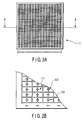
- FIG. 2A and FIG. 2B are views to schematically explain the structure of the image sensor 10.
- FIG. 2A is a view showing an upper surface of the image sensor 10 (and an upper surface of the sensor element array 11).
- FIG. 2B is an enlarged view showing a portion surrounded by a circle shown in FIG. 2A.
- FIG. 3A is a cross-sectional view taken along the line A-A of the image sensor 10 shown in FIG. 2A.
- the sensor element array 11 has a CdTe element 110, a first electrode 111, a second electrode 112, and an active contact 113.
- the CdTe element 110 is a compound semiconductor consisting of Cd (cadmium) and Te (tellurium).
- the energy gap of the CdTe element 110 is about 1.47 eV under room temperature.
- the first electrode 111 is arrayed like two-dimensional matrix on the radiation incident side of the CdTe element 110, and is formed of Pt, for example.
- the second electrode 112 is arrayed on an electric signal fetch side of the CdTe element 110 facing the first electrode 111 via the CdTe element 110, and is formed of Pt, for example.
- a predetermined voltage for detecting radiation is applied between the first and second electrodes 111 and 112.
- the sensor element array 11 is formed in the following manner.
- the sensor element is formed in a manner of sandwiching the CdTe element 110 between the first and second Pt electrodes 111 and 112, and thereafter, in a two-dimensional matrix.
- a depletion layer formed by applying the voltage between the first and second Pt electrodes 111 and 112
- many electrons and holes are generated along the track of radiation.
- Positive and negative charges are fetched as an electric signal, and thereby, the sensor array element 11 generates image information based on the incident radiation.
- the active contact 113 is formed in the first and second electrodes, and is a pad for flip-chip-mounting the sensor array element 11 on the IC substrate 15 by the stud bump process described later.
- the electric signal detected by each sensor element is inputted to the IC from the active contact 113 via a stud bump described later, thereafter, is subjected to predetermined signal processing such as amplification.
- FIG. 3 is a view to schematically explain the structure of the IC substrate 15 included in the image sensor 10.
- FIG. 4A is a view showing an upper surface of the IC substrate 15, and
- FIG. 4B is an enlarged view showing a portion surrounded by a circle shown in FIG. 4A.
- FC pad flip chip bump 150 included in each of plural X-ray resistant ICs (not shown) is arrayed like two-dimensional matrix.
- the position of the FC pad 150 corresponds to that of the above active contact 113, and FC mounting is carried out based on both positions.
- a stud bump described later is formed on the FC pad 150.
- FIG. 3B and FIG. 3C are views to explain FC mounting of the image sensor 10 to the IC substrate 15.
- FIG. 3B is an enlarged view showing part of the connecting layer 13 shown in FIG. 3A.
- the connecting layer 13 has a stud bump 130, an indium layer 131 formed at the distal end of the stud bump 130, and an insulating layer 132.
- the stud bump 130 is formed on the FC pad 150 on each IC substrate 15, and is made of gold.
- the stud bump 130 is formed in a manner that a projection-shaped bump is laminated on the FC pad 150 in one or two-stage or more.
- the stud bump 130 performs the function of absorbing the current application between the sensor element and the IC, and a connection error in FC mounting described later. Therefore, it is preferable that the material used for the stud bump is a relatively soft metal having excellent conductivity.
- the indium layer (In layer) 131 is a thin film layer, which is formed at the distal end of the stud bump 130.
- the indium layer 131 is formed into a tapered shape so as to have a predetermined height in the manufacturing stage (see FIG. 7).
- the indium layer 131 is pressed and welded by the second electrode and the active contact 113, and thus, has a shape shown in FIG. 3C.
- the indium layer 131 performs the function of applying a current between the sensor element and the IC, and providing a predetermined height required for FC mounting described later.
- a solder having a melting point of 100°C or less is used.
- bismuth may be used in addition to indium.
- the insulating layer 132 is a resin layer formed in underfill, and is formed of an epoxy resin, for example. Further, the insulating layer 132 performs the function of burying the stud bump 130 and the indium layer 131 so that they can be both electrically insulated and reinforced. The insulating layer 132 prevents the thermal stress generated by the difference in thermal expansion coefficient between the sensor element array 11 and the IC substrate 15 from concentrating on the stud bump 130 and the indium layer 131.
- the sensor element array 11 and the IC substrate 15 are mounted in the laminated form by the connection layer 13, in particular, the stud bump 130 and the In layer 131. More specifically, in the conventional image sensor, the IC and the sensor element arrayed on the same plane are connected by wire bonding; a so-called "two-dimensional mounting mode" has been employed. On the contrary, in the image sensor 10, the sensor element array 11 is laminated on the IC substrate 15 by the stud bump 130 and the In layer 131; a so-called "three-dimensional mounting mode" is employed.
- the image sensor made employing the above three-dimensional mounting IC connection is made from the lower portion of each sensor element. Therefore, even if the number of sensor elements increases, it is possible to easily extract signals. As a result, it is possible to generate an image having a great number of pixels as compared with the conventional case. Further, the three-dimensional mounting is employed, and thereby, it is possible to down-size the image sensor.
- FIG. 5 is a flowchart schematically showing the method of manufacturing the image sensor 10.
- the IC substrate 15 having the plurality of ICs arrayed in a predetermined form is prepared.
- a stub bump (hereinafter, referred to as "Au stud bump") using gold as the base material is molded on each flip chip pad 150 (step S1).
- the au stub bump is formed in plural stages (i.e., the Au stud bump is laminated).
- a stainless substrate is plated with indium (In) so as to form the transfer destination for indium (In) transfer to the distal end of the Au stud bump (step S1').
- step S2 the indium (In) is transferred to the distal end of the Au stud bump.
- the transfer in step S2 is carried out in the following manner using an FC bonder.
- FIG. 6 is a conceptual view to explain the indium (In) transfer in step S2.
- the IC substrate 15 with the Au stud bump 130 provided on the head side of the FC bonder (not shown) is pressed against a stainless substrate 16 plated with In.
- the above pressing operation is carried out under predetermined head temperature control, predetermined head speed and predetermined load control, and further, there is the case where the pressing operation is repeated plural times. After a predetermined pressing time elapses, when the head is pulled up under predetermined head temperature control, predetermined head speed and predetermined load control, the In transfer to the distal end of the Au stud bump 130 is completed.
- FIG. 7 is a view schematically showing the In layer 131 formed at the distal end of the Au stud bump 130 formed in the process of step S2.
- the In layer 131 formed in step S2 has a tapered shape and a predetermined height. Also, the shape of the Au stud bump 130 does not crush as shown in FIG. 3C.
- step S3 FC mounting of the sensor element array 11 to the IC substrate 15 is carried out. More specifically, first, flattening is carried out with respect to the In layer 131 formed in step S2. This is to prevent an extra pressure from being applied to one point on the second electrode of the sensor element array 11 (in other words, pressure is uniformly applied to each second electrode 112). After the above flattening, the pressing/heating by the FC bonder destroys/melts an oxide film on the surface of each In layer 131 so that the In layer 131 can be welded to the corresponding second electrode 112, and thereby, FC welding is achieved between the sensor element array 11 and the IC substrate 15. In this case, no gap is generated between the second electrode 112 and the In layer 131 by the above press.
- the insulating layer 132 is formed (step S4). More specifically, the underfill seals the gap (FC gap) between the sensor element array 11 and the IC substrate 15, which have been FC-connected in the process of step S3. Thereafter, the underfill is heated and hardened for a predetermined time so that the insulating layer 132 can be formed.
- FIG. 8 is a flowchart showing the embodiment of the method of manufacturing the image sensor 10.
- the IC substrate 15 having the plurality of ICs arranged in a predetermined form is prepared.
- a stub bump (hereinafter, referred to as "Au stud bump") using gold as the base material is molded on each flip chip pad 150 (step S1).
- the stainless substrate is plated with indium (In) to a thickness of 20 ⁇ m, and thus, the transfer destination for In transfer to the distal end of the Au stud bump is formed (step S1')
- step S2 the indium (In) is transferred to the distal end of the Au stud bump.
- the transfer in step S2 is carried out in the following manner using an FC bonder.
- the IC substrate with the stud bump 150 is set to the head side of the FC bonder.
- the stainless substrate plated with indium (In) is set to the table side.
- the table temperature is kept at 50°C, for example.
- the head is pressed at loading: 2.64 [Hgf], pressing time: 11.0 sec., head temperature: 250°C, and head pull-down speed 0.2 [mm/s], and thereafter, pulled up by the height of 5 mm at the pull-up speed of 0.5 [mm/s] while maintaining the head temperature.
- the In plating layer is left to cool for 40 seconds, and then, the second-pressing is carried out under the following conditions. That is, the head is pressed at loading: 2.64 [Hgf], pressing time: 5.0 sec., head temperature: 250°C, and head pull-down speed 0.2 [mm/s], and thereafter, pulled up by the height of 5 mm at the pull-up speed of 0.08 [mm/s] while maintaining the head temperature.
- the In transfer to the distal end of the Au stud bump 130 is then completed.
- step S3 Sequentially, FC mounting of the sensor element array 11 to the IC substrate 15 is carried out.
- step S2 flattening is carried out with respect to the In layer 131 formed in step S2.
- the IC substrate 15 is set to the head side of the FC bonder; on the other hand, the sensor element array 11 is set to the table side.
- the head is pulled down under the following conditions, that is, at loading: 10.00 [Hgf], head temperature: 175°C, pressing time: 10.0 sec., and head pull-down speed 0.08 [mm/s]. Thereafter, the head is pressed against the stud bump 130 and the active contact 113 of the In layer 131 under the following conditions. After the above press is completed, the head position is held for 1.0 second while maintaining the head temperature at 175°C.
- the head is pulled up by the height of 5 mm at the pull-up speed of 0.17 [mm/s] while keeping the head temperature at 175°C, and thereby, the sensor element array 11 and the IC substrate 15 can be FC-welded together.
- the table temperature is kept at 80°C.
- the insulating layer 132 is formed (step S4).
- the sensor element array 11 is heated at a temperature from 60°C to 80°C, and an epoxy resin is kept at a temperature from 25°C to 40°C.
- the epoxy resin is injected into the FC gap formed in the process of step S3. In this case, care must be taken to prevent the sensor element array comprising CdTe and the FC welding portion separating.
- the heating temperature of the sensor element array 11 must be set so as not to exceed 80°C. If the temperature exceeds 80°C, the epoxy resin is set faster; as a result, injection is not smoothly achieved.
- the injection processing is carried out for about 3 minutes.
- heating and hardening are carried out under the condition that the heating temperature is 125°C and the heating time is two hours, and thereby, the insulating layer 132 is formed.
- the Au stud bump 130 (plural-stage Au stud bump 130, as the case may be,) and the In layer 131 having a predetermined height, formed at the distal end of the Au stud bump 130. More specifically, the height of the In layer 131 further increases in addition to the height of the au stud bump 130. By doing so, it is possible to obtain a larger pressing width when pressure-welding the sensor element array 11 to the IC substrate 15 in FC welding. Further, the Au stud bump 130 absorbs the error in the height between bumps connected in FC welding. Therefore, according to the manufacturing method, it is possible to readily realize an image sensor having a great number of pixels.
- the image sensor 10 can be provided at low cost as compared with the conventional case.
- the image sensor 10 uses the CdTe element, it is possible to provide a high-performance image sensor as compared with the conventional case.
- the stud bump process has been described while giving the image sensor 10 using the CdTe element as one example.
- the stud bump process is applicable to the method of manufacturing the image sensors using the base materials other than CdTe as the sensor element; for example, Si, Ge, CdZnTe or HgCdTe (mercury cadmium telluride).
- the present invention is not limited to the above embodiment, and various modifications may be made without departing from the scope of the general inventive concept in the working stage of the invention.
- Each embodiment may be carried out based on proper combinations as much as possible; in this case, combined effects are obtained.
- the above embodiment includes various-step inventions, and the plurality of constituent requirements disclosed is properly combined, and thereby, various inventions can be extracted. For example, even if some constituent requirements are deleted from all constituent requirements disclosed in the embodiment, it is possible to solve the problem described in the column of the problem that the invention is to solve. When at least one of the effects described in the column of the effects of the invention is obtained, the construction in which the constituent requirements is deleted can be extracted as an invention.
- the image sensor has many sensor elements, it is possible to realize a highly sensitive image sensor, which can readily make electric connection between each sensor element and amplification IC, and to provide a method of manufacturing the image sensor.
Landscapes
- Solid State Image Pick-Up Elements (AREA)
- Measurement Of Radiation (AREA)
Abstract
Description
Claims (10)
- An image sensor comprising:a sensor element array having a plurality of sensor elements arrayed in a two-dimensional matrix;an IC substrate laminating said sensor element array and provided with a plurality of ICs for amplifying an electric signal based on radiation incident on any of the plurality of said sensor elements; anda connection layer interposed between said sensor element array and said IC substrate, and electrically connecting each electrode of said sensor elements with each electrode of said ICs.
- The image sensor according to claim 1, wherein said connection layer has a plurality of stud bumps formed on an electrode of each of the plurality of said ICs;
and a plurality of thin film layers formed at the distal end of each of the plurality of said stud bumps and electrically connected with the electrode of each of the plurality of said sensor elements. - The image sensor according to claim 2, wherein each of said stud bumps is made of gold; and
each of said thin film layers is made of indium. - The image sensor according to claim 2, wherein said connection layer has an insulating layer which buries said stud bumps and said thin film layers.
- The image sensor according to claim 1, wherein said connection layer has a plurality of multi-layer bumps formed in a manner that at least two-layer stud bump is laminated on the electrode of each of the plurality of said ICs, and a plurality of thin film layers formed at the distal end of said multi-layer bump and electrically connected with the electrode of each of the plurality of said sensor elements.
- The image sensor according to claim 5, wherein each of said multi-layer bumps is made of gold;
and each of said thin film layers is made of indium. - The image sensor according to claim 5, wherein said connection layer has an insulating layer which buries said stud bumps and said thin film layers.
- The image sensor according to claim 1, wherein said sensor element is a CdTe element.
- A method of manufacturing an image sensor comprising the following steps of:forming stud bumps on each electrode pad of the predetermined number of IC chips provided in a first substrate;carrying out indium plating with respect to a second substrate;transferring said plated indium to said second substrate to the distal end of each of said stud bumps so that a plurality of thin film layers can be formed;connecting each of said thin film layers with the electrode of each of sensor elements so that a sensor element array having the plurality of said sensor elements arrayed like two-dimensional matrix is mounted to each of IC chips of said first substrate by flip chip mounting; andinjecting an insulating resin between said first substrate and said sensor element array, and thereafter, hardening said insulating resin.
- The method of manufacturing said image sensor, according to claim 9, wherein each of said stud bumps is made of gold, and each of said thin film layers is made of indium.
Applications Claiming Priority (3)
| Application Number | Priority Date | Filing Date | Title |
|---|---|---|---|
| JP2001057346 | 2001-03-01 | ||
| JP2001057346A JP2002261262A (en) | 2001-03-01 | 2001-03-01 | Image sensor and method of manufacturing the same |
| PCT/JP2002/001919 WO2002071489A1 (en) | 2001-03-01 | 2002-03-01 | Image sensor and production method therefore |
Publications (2)
| Publication Number | Publication Date |
|---|---|
| EP1365453A1 true EP1365453A1 (en) | 2003-11-26 |
| EP1365453A4 EP1365453A4 (en) | 2008-04-30 |
Family
ID=18917238
Family Applications (1)
| Application Number | Title | Priority Date | Filing Date |
|---|---|---|---|
| EP02701675A Ceased EP1365453A4 (en) | 2001-03-01 | 2002-03-01 | IMAGE SENSOR AND METHOD OF MANUFACTURING THE SAME |
Country Status (4)
| Country | Link |
|---|---|
| US (3) | US20030116816A1 (en) |
| EP (1) | EP1365453A4 (en) |
| JP (1) | JP2002261262A (en) |
| WO (1) | WO2002071489A1 (en) |
Cited By (1)
| Publication number | Priority date | Publication date | Assignee | Title |
|---|---|---|---|---|
| WO2010094315A1 (en) | 2009-02-20 | 2010-08-26 | Espros Photonics Ag | Flip-chip soldering method, and circuit comprising a soldered semiconductor chip which is contacted using flip-chip technology |
Families Citing this family (6)
| Publication number | Priority date | Publication date | Assignee | Title |
|---|---|---|---|---|
| JP2002261262A (en) | 2001-03-01 | 2002-09-13 | Mitsubishi Heavy Ind Ltd | Image sensor and method of manufacturing the same |
| JP4345403B2 (en) * | 2003-08-21 | 2009-10-14 | セイコーエプソン株式会社 | Image reading device |
| JP4379295B2 (en) | 2004-10-26 | 2009-12-09 | ソニー株式会社 | Semiconductor image sensor module and manufacturing method thereof |
| US7589324B2 (en) * | 2006-12-21 | 2009-09-15 | Redlen Technologies | Use of solder mask as a protective coating for radiation detector |
| CN101903802B (en) * | 2007-12-20 | 2013-09-11 | 皇家飞利浦电子股份有限公司 | Direct conversion detector |
| JP5292939B2 (en) * | 2008-06-20 | 2013-09-18 | ソニー株式会社 | Image processing apparatus and method, and manufacturing apparatus |
Family Cites Families (24)
| Publication number | Priority date | Publication date | Assignee | Title |
|---|---|---|---|---|
| US5043582A (en) | 1985-12-11 | 1991-08-27 | General Imagining Corporation | X-ray imaging system and solid state detector therefor |
| US5071787A (en) * | 1989-03-14 | 1991-12-10 | Kabushiki Kaisha Toshiba | Semiconductor device utilizing a face-down bonding and a method for manufacturing the same |
| JPH05166879A (en) | 1991-12-12 | 1993-07-02 | Matsushita Electric Ind Co Ltd | IC mounting method |
| KR0137190B1 (en) * | 1992-12-03 | 1998-04-28 | 모리시타 요이찌 | Fully Closed Image Sensor and Fully Closed Image Sensor Unit |
| FR2715002B1 (en) * | 1994-01-07 | 1996-02-16 | Commissariat Energie Atomique | Electromagnetic radiation detector and its manufacturing process. |
| GB2289983B (en) * | 1994-06-01 | 1996-10-16 | Simage Oy | Imaging devices,systems and methods |
| JPH08115946A (en) * | 1994-10-13 | 1996-05-07 | Matsushita Electric Ind Co Ltd | Flip chip mounting method |
| JP3243956B2 (en) * | 1995-02-03 | 2002-01-07 | 松下電器産業株式会社 | Semiconductor device and manufacturing method thereof |
| JP2985731B2 (en) | 1995-05-31 | 1999-12-06 | 松下電器産業株式会社 | X-ray imaging device |
| US5650667A (en) * | 1995-10-30 | 1997-07-22 | National Semiconductor Corporation | Process of forming conductive bumps on the electrodes of semiconductor chips using lapping and the bumps thereby created |
| US5723866A (en) * | 1996-06-26 | 1998-03-03 | He Holdings, Inc. | Method for yield and performance improvement of large area radiation detectors and detectors fabricated in accordance with the method |
| JPH1022337A (en) * | 1996-07-04 | 1998-01-23 | Hitachi Ltd | Semiconductor chip bonding method |
| GB2319394B (en) * | 1996-12-27 | 1998-10-28 | Simage Oy | Bump-bonded semiconductor imaging device |
| JPH10233401A (en) * | 1997-02-19 | 1998-09-02 | Ricoh Co Ltd | Semiconductor device |
| JPH1126502A (en) * | 1997-07-01 | 1999-01-29 | Matsushita Electric Ind Co Ltd | Bump leveling method |
| TW398045B (en) * | 1997-10-02 | 2000-07-11 | Matsushita Electric Industrial Co Ltd | Method for mounting semiconductor element to circuit board, and semiconductor device |
| JP3545247B2 (en) * | 1998-04-27 | 2004-07-21 | シャープ株式会社 | 2D image detector |
| JP2000100874A (en) | 1998-09-21 | 2000-04-07 | Sony Corp | Flip chip manufacturing apparatus and flip chip manufacturing method |
| JP2001074847A (en) * | 1999-07-08 | 2001-03-23 | Canon Inc | Radiation imaging apparatus and radiation imaging system |
| US6593168B1 (en) * | 2000-02-03 | 2003-07-15 | Advanced Micro Devices, Inc. | Method and apparatus for accurate alignment of integrated circuit in flip-chip configuration |
| US6348399B1 (en) * | 2000-07-06 | 2002-02-19 | Advanced Semiconductor Engineering, Inc. | Method of making chip scale package |
| US6658082B2 (en) * | 2000-08-14 | 2003-12-02 | Kabushiki Kaisha Toshiba | Radiation detector, radiation detecting system and X-ray CT apparatus |
| JP2002261262A (en) | 2001-03-01 | 2002-09-13 | Mitsubishi Heavy Ind Ltd | Image sensor and method of manufacturing the same |
| US6510195B1 (en) * | 2001-07-18 | 2003-01-21 | Koninklijke Philips Electronics, N.V. | Solid state x-radiation detector modules and mosaics thereof, and an imaging method and apparatus employing the same |
-
2001
- 2001-03-01 JP JP2001057346A patent/JP2002261262A/en active Pending
-
2002
- 2002-03-01 WO PCT/JP2002/001919 patent/WO2002071489A1/en not_active Ceased
- 2002-03-01 EP EP02701675A patent/EP1365453A4/en not_active Ceased
- 2002-12-13 US US10/318,122 patent/US20030116816A1/en not_active Abandoned
-
2004
- 2004-06-21 US US10/871,029 patent/US7041981B2/en not_active Expired - Lifetime
-
2005
- 2005-03-08 US US11/073,730 patent/US6992297B2/en not_active Expired - Lifetime
Cited By (2)
| Publication number | Priority date | Publication date | Assignee | Title |
|---|---|---|---|---|
| WO2010094315A1 (en) | 2009-02-20 | 2010-08-26 | Espros Photonics Ag | Flip-chip soldering method, and circuit comprising a soldered semiconductor chip which is contacted using flip-chip technology |
| DE102009009813A1 (en) | 2009-02-20 | 2010-08-26 | Espros Photonics Ag | Soldering and circuit |
Also Published As
| Publication number | Publication date |
|---|---|
| JP2002261262A (en) | 2002-09-13 |
| WO2002071489A1 (en) | 2002-09-12 |
| US20040232346A1 (en) | 2004-11-25 |
| US20030116816A1 (en) | 2003-06-26 |
| EP1365453A4 (en) | 2008-04-30 |
| US20050151088A1 (en) | 2005-07-14 |
| US6992297B2 (en) | 2006-01-31 |
| US7041981B2 (en) | 2006-05-09 |
Similar Documents
| Publication | Publication Date | Title |
|---|---|---|
| US7223981B1 (en) | Gamma ray detector modules | |
| US6933505B2 (en) | Low temperature, bump-bonded radiation imaging device | |
| EP0948810B1 (en) | Bump-bonded semiconductor imaging device | |
| US6372549B2 (en) | Semiconductor package and semiconductor package fabrication method | |
| KR100647212B1 (en) | Conductive adhesive bonded semiconductor substrates for radiation imaging devices | |
| US4943491A (en) | Structure for improving interconnect reliability of focal plane arrays | |
| WO2006057097A1 (en) | Semiconductor device | |
| US11682745B2 (en) | Photon detector array assembly | |
| US7041981B2 (en) | Image sensor and manufacturing method thereof | |
| US5904495A (en) | Interconnection technique for hybrid integrated devices | |
| US6218629B1 (en) | Module with metal-ion matrix induced dendrites for interconnection | |
| JP2019523402A (en) | DETECTOR MODULE, DETECTOR, IMAGING DEVICE AND DETECTOR MODULE MANUFACTURING METHOD | |
| JP7858316B2 (en) | Electronic module, apparatus, and method for manufacturing an electronic module | |
| JP4397012B2 (en) | Semiconductor image sensor having hole-type electrode and manufacturing method thereof | |
| JP2005520346A (en) | Pixel sensor array and manufacturing method thereof | |
| CN112385025A (en) | Stacked semiconductor device and plurality of chips used for the same | |
| JP4799746B2 (en) | Radiation detector module | |
| KR100311979B1 (en) | infrared detector and method for manufacturing the same | |
| CN118538741A (en) | A detector imaging module and packaging process | |
| TWI338364B (en) | Image sensor chip package structure and method thereof | |
| JPH0536960A (en) | Image sensor manufacturing method | |
| JP2006196525A (en) | Light or radiation detector and method for manufacturing the same | |
| RU2515190C1 (en) | METHOD OF MAKING PHOTODETECTOR MODULE BASED ON PbSe | |
| Capote et al. | Gamma ray detector modules | |
| JPH0744251B2 (en) | Semiconductor device |
Legal Events
| Date | Code | Title | Description |
|---|---|---|---|
| PUAI | Public reference made under article 153(3) epc to a published international application that has entered the european phase |
Free format text: ORIGINAL CODE: 0009012 |
|
| 17P | Request for examination filed |
Effective date: 20021219 |
|
| AK | Designated contracting states |
Kind code of ref document: A1 Designated state(s): DE FR GB IT |
|
| RAP1 | Party data changed (applicant data changed or rights of an application transferred) |
Owner name: JAPAN AEROSPACE EXPLORATION AGENCY Owner name: MITSUBISHI HEAVY INDUSTRIES, LTD. |
|
| A4 | Supplementary search report drawn up and despatched |
Effective date: 20080401 |
|
| RIC1 | Information provided on ipc code assigned before grant |
Ipc: H01L 27/146 20060101AFI20080326BHEP Ipc: H01L 21/60 20060101ALI20020917BHEP |
|
| 17Q | First examination report despatched |
Effective date: 20080716 |
|
| STAA | Information on the status of an ep patent application or granted ep patent |
Free format text: STATUS: THE APPLICATION HAS BEEN REFUSED |
|
| 18R | Application refused |
Effective date: 20100708 |