EP1365449A2 - Metallic strain-absorbing layer for improved fatigue resistance of solder-attached devices - Google Patents
Metallic strain-absorbing layer for improved fatigue resistance of solder-attached devices Download PDFInfo
- Publication number
- EP1365449A2 EP1365449A2 EP03101352A EP03101352A EP1365449A2 EP 1365449 A2 EP1365449 A2 EP 1365449A2 EP 03101352 A EP03101352 A EP 03101352A EP 03101352 A EP03101352 A EP 03101352A EP 1365449 A2 EP1365449 A2 EP 1365449A2
- Authority
- EP
- European Patent Office
- Prior art keywords
- alloy
- layer
- nickel
- titanium
- solder
- Prior art date
- Legal status (The legal status is an assumption and is not a legal conclusion. Google has not performed a legal analysis and makes no representation as to the accuracy of the status listed.)
- Withdrawn
Links
Images


Classifications
-
- H—ELECTRICITY
- H10—SEMICONDUCTOR DEVICES; ELECTRIC SOLID-STATE DEVICES NOT OTHERWISE PROVIDED FOR
- H10W—GENERIC PACKAGES, INTERCONNECTIONS, CONNECTORS OR OTHER CONSTRUCTIONAL DETAILS OF DEVICES COVERED BY CLASS H10
- H10W72/00—Interconnections or connectors in packages
- H10W72/01—Manufacture or treatment
- H10W72/019—Manufacture or treatment of bond pads
-
- H—ELECTRICITY
- H10—SEMICONDUCTOR DEVICES; ELECTRIC SOLID-STATE DEVICES NOT OTHERWISE PROVIDED FOR
- H10W—GENERIC PACKAGES, INTERCONNECTIONS, CONNECTORS OR OTHER CONSTRUCTIONAL DETAILS OF DEVICES COVERED BY CLASS H10
- H10W72/00—Interconnections or connectors in packages
- H10W72/01—Manufacture or treatment
- H10W72/012—Manufacture or treatment of bump connectors, dummy bumps or thermal bumps
-
- H—ELECTRICITY
- H10—SEMICONDUCTOR DEVICES; ELECTRIC SOLID-STATE DEVICES NOT OTHERWISE PROVIDED FOR
- H10W—GENERIC PACKAGES, INTERCONNECTIONS, CONNECTORS OR OTHER CONSTRUCTIONAL DETAILS OF DEVICES COVERED BY CLASS H10
- H10W72/00—Interconnections or connectors in packages
- H10W72/071—Connecting or disconnecting
- H10W72/072—Connecting or disconnecting of bump connectors
- H10W72/07251—Connecting or disconnecting of bump connectors characterised by changes in properties of the bump connectors during connecting
- H10W72/07252—Connecting or disconnecting of bump connectors characterised by changes in properties of the bump connectors during connecting changes in structures or sizes
-
- H—ELECTRICITY
- H10—SEMICONDUCTOR DEVICES; ELECTRIC SOLID-STATE DEVICES NOT OTHERWISE PROVIDED FOR
- H10W—GENERIC PACKAGES, INTERCONNECTIONS, CONNECTORS OR OTHER CONSTRUCTIONAL DETAILS OF DEVICES COVERED BY CLASS H10
- H10W72/00—Interconnections or connectors in packages
- H10W72/20—Bump connectors, e.g. solder bumps or copper pillars; Dummy bumps; Thermal bumps
- H10W72/221—Structures or relative sizes
-
- H—ELECTRICITY
- H10—SEMICONDUCTOR DEVICES; ELECTRIC SOLID-STATE DEVICES NOT OTHERWISE PROVIDED FOR
- H10W—GENERIC PACKAGES, INTERCONNECTIONS, CONNECTORS OR OTHER CONSTRUCTIONAL DETAILS OF DEVICES COVERED BY CLASS H10
- H10W72/00—Interconnections or connectors in packages
- H10W72/20—Bump connectors, e.g. solder bumps or copper pillars; Dummy bumps; Thermal bumps
- H10W72/251—Materials
-
- H—ELECTRICITY
- H10—SEMICONDUCTOR DEVICES; ELECTRIC SOLID-STATE DEVICES NOT OTHERWISE PROVIDED FOR
- H10W—GENERIC PACKAGES, INTERCONNECTIONS, CONNECTORS OR OTHER CONSTRUCTIONAL DETAILS OF DEVICES COVERED BY CLASS H10
- H10W72/00—Interconnections or connectors in packages
- H10W72/20—Bump connectors, e.g. solder bumps or copper pillars; Dummy bumps; Thermal bumps
- H10W72/251—Materials
- H10W72/252—Materials comprising solid metals or solid metalloids, e.g. PbSn, Ag or Cu
-
- H—ELECTRICITY
- H10—SEMICONDUCTOR DEVICES; ELECTRIC SOLID-STATE DEVICES NOT OTHERWISE PROVIDED FOR
- H10W—GENERIC PACKAGES, INTERCONNECTIONS, CONNECTORS OR OTHER CONSTRUCTIONAL DETAILS OF DEVICES COVERED BY CLASS H10
- H10W72/00—Interconnections or connectors in packages
- H10W72/90—Bond pads, in general
- H10W72/921—Structures or relative sizes of bond pads
- H10W72/923—Bond pads having multiple stacked layers
-
- H—ELECTRICITY
- H10—SEMICONDUCTOR DEVICES; ELECTRIC SOLID-STATE DEVICES NOT OTHERWISE PROVIDED FOR
- H10W—GENERIC PACKAGES, INTERCONNECTIONS, CONNECTORS OR OTHER CONSTRUCTIONAL DETAILS OF DEVICES COVERED BY CLASS H10
- H10W72/00—Interconnections or connectors in packages
- H10W72/90—Bond pads, in general
- H10W72/941—Dispositions of bond pads
- H10W72/9415—Dispositions of bond pads relative to the surface, e.g. recessed, protruding
Definitions
- the present invention is related in general to the field of semiconductor devices and processes and more specifically to the structure of metallurgical interconnection pads for flip-chip assembly of semiconductor devices.
- Chip-Scale Package Chip-Scale Package
- the chip-to-be-flipped may be attached to a second interconnection surface such as an interposer, or alternatively, coupled directly to a printed circuit board (PCB). Attaching the flip-chip to the next interconnect is carried out by aligning the solder bumps or balls on the chip to contact pads on the second level interconnection and then performing a second solder reflow operation. During the reflow, the bumps or balls liquefy and make a bond to the next interconnect level which has pads or traces to receive the solder.
- a second interconnection surface such as an interposer, or alternatively, coupled directly to a printed circuit board (PCB). Attaching the flip-chip to the next interconnect is carried out by aligning the solder bumps or balls on the chip to contact pads on the second level interconnection and then performing a second solder reflow operation. During the reflow, the bumps or balls liquefy and make a bond to the next interconnect level which has pads or traces to receive the solder.
- flip-chips often use a polymeric underfill between the chip and the interposer or PCB to alleviate mechanical stress caused by the mismatch in the coefficients of thermal expansion (CTE) between the semiconductor chip, the interposer, if any, and the PCB.
- CTE coefficients of thermal expansion
- Many reliability problems occur due to the stress placed on the solder bumps or balls when the integrated circuit is cycled from hot to cool during operation.
- this second set may also be affected by similar stress and reliability problems.
- Another method aims at absorbing part of the thermomechanical stress on the solder joints by plastic material surrounding the joints and filling the gap between chip and substrate. See for instance, U. S. Patents # 6,228,680, issued on May 8, 2001; # 6,213,347, issued on Apr. 10, 2001, and # 6,245,583, issued on Jun. 12, 2001 (Thomas et al., Low Stress Method and Apparatus for Underfilling Flip-Chip Electronic Devices).
- the underfilling method represents an unwelcome process step after device attachment to the motherboard.
- Another method applies a polymer layer on top of the protective overcoat with the aim of reducing the stress to the overcoat perimeter and the dielectric material underlying the contact pad. See for instance the publication "A Silicon and Aluminum Dynamic Memory Technology” by Richard A. Larsen (IBM J. Res. Develop., vol.24, May 1980, pp. 268-282).
- the article includes description of a flip-chip packaging technology using a solder bump on an under-bump metallization, which is resting its perimeter on a thick polyimide layer. The bump structure is often supported by another polyimide layer.
- An integrated circuit chip which has a plurality of contact pads to be connected by reflow attachment to outside parts.
- the chip comprises a deposited layer of nickel/titanium alloy on each of the pads; the alloy has a composition and crystalline structure operable in reversible phase transitions under thermomechanical stress, whereby mechanical strain is absorbed by the alloy layer.
- the alloy has between 55.0 and 56.0 weight% nickel, between 44.0 and 45.0 weight% titanium, and a thickness in the range from ⁇ 0.3 to 6.0 ⁇ m, recrystallized after deposition in a temperature range from 450 to 600 °C for a time period between 4 and 6 min.
- a layer of solderable metal is on the alloy, operable as diffusion barrier after reflow attachment.
- the geometries of the nickel/titanium layer and the reflow attachment are the same at the location of the highest stress.
- the crystalline structure of the nickel/titanium is martensite, having a Lower Superelastic Plateau Stress (yield stress) lower than the yield stress of the reflow attachment selected.
- yield stress Superelastic Plateau Stress
- the preferred alloy of the present invention has 55.5 ⁇ 0.5 weight% nickel (Ni) and 44.5 ⁇ 0.5 weight% titanium (Ti) (and maximal 0.05 % oxygen, iron, and carbon each).
- the NiTi and the reflow alloy are jointly selected so that at the lower temperatures of the temperature cycle, the NiTi is martensitic with a yield strength below the yield strength of the reflow alloy. Consequently, the NiTi will yield preferentially.
- the NiTi will turn austenitic with a yield strength higher than the reflow alloy. Consequently, the reflow alloy will yield preferentially.
- the net effect of this trade-off in the joint yielding characteristic is an improvement of the total number of temperature cycles to failure.
- the plastic deformation is distributed over a larger volume of materials.
- NiTi layers for IC chips and recrystallization to achieve martensite/austenite transformation in the temperature range of electronic device application are essential aspects of the present invention.
- NiTi is applied on each device contact pad as a thin layer together with an outside solderable layer.
- the bulk of the interconnection of the device to an external part (such as a printed circuit board made of FR4), is still a reflowable solder "ball" of a suitable tin alloy.
- An example of how the invention functions can be seen in a typical qualification test: After attachment of the device to the board, the system is subjected to repeated temperature cycles from -40 to +125 °C in 15 min ramps, causing a strain rate of about 13 ⁇ 10E-6/°C due to the difference of the coefficients of thermal expansion between the silicon chip and the FR4 board.
- the NiTi lower superelastic stress In the temperature cycle from -40 to +125 °C, the NiTi lower superelastic stress must be below the solder yield stress in order to be effective for postponing failures.
- the solder yield stress has been published, for two preferred tin alloy solders 63Sn/37Pb and 95.75/Sn3.5Ag/ 0.75Cu, by Masazumi Amagai in "Chip Scale Package Solder Joint Reliability Modeling and Material Characterization" (J. Japan Inst. Electronics Packaging, vol.3, no.1., pp. 45-56, Jan. 2000). Using these data and plotting the yield stress for these two solder alloys in the temperature interval from -40 to +125 °C, results in FIG. 3. The yield stress is measured in MPa.
- Another aspect of the invention is to provide the stress-relieving structure of the device interconnection comprising the TiNi layer.
- Another aspect of the invention is to provide the process flow for the fabrication of the TiNi layer and the complete interconnection structure.
- solder alloys can be employed for the provided TiNi layers and techniques.
- NiTi The fundamental characteristics of NiTi have been summarized in "Biocompatibility Evaluation of Nickel-Titanium Shape Memory Metal Alloy", by Jorma Ryhanen, Univ. of Oulu, Finland, May 7, 1999.
- the preferred NiTi alloy can exist in two different temperature-dependent crystal structures, "martensite” at lower temperature and "austenite” at higher temperature. Austensite has a simple cubic structure, is strong and hard; martensite has a more complex rhombic structure, is ductile and can be deformed; the elongation to failure is over 25 %.
- FIG. 1 the percent austenite is plotted schematically as a function of temperature. As illustrated in FIG.
- FIG. 2 deformation of a solid body is plotted as caused by increasing force.
- Hookian elasticity range is surpassed by increasing outside force or stress, most metals and alloys deform by slip or dislocation (irreversible change) (see FIG. 2A).
- NiTi responds to stress by changing the orientation of its crystal structure (twinning), where the martensite variants have 24 cystallographically equivalent planes correspond to only one possible austenite parent phase.
- a NiTi specimen will deform until it consists only of the correspondence variant which produces maximum strain (reversible change).
- Superelasticity refers to the ability if NiTi to return to its original shape upon unloading after a substantial deformation (see FIG. 2B). This ability is based on stress-induced martensite formation.
- the application of an outer stress causes martensite to form at temperatures higher than Ms (see FIG. 1).
- the macroscopic deformation is accommodated by the formation of martensite.
- the NiTi lower superelastic plateau stress must be below the solder yield stress in order to be effective for postponing failures.
- the solder yield stress has been published, for two preferred tin alloy solders 63Sn/37Pb (eutectic) and 95.75/Sn3.5Ag/ 0.75Cu (lead-free), by Masazumi Amagai in "Chip Scale Package Solder Joint Reliability Modeling and Material Characterization" (J. Japan Inst. Electronics Packaging, vol.3, no.1., pp. 45-56, Jan. 2000).
- yield stress refers to the stress at which normal material leaves the elastic regime and enters the plastic regime.
- the yield stress increases strongly in the lower temperature regime 301 (below approximately 10 °C) for both solder alloys.
- the higher temperature regime 302 above approximately 10 °C
- the yield stress changes relatively less with temperature.
- the NiTi and the reflow alloy are jointly selected so that in the lower temperature regime 301 of the temperature cycle, the NiTi is martensitic with a lower suprelastic plateau stress below the yield stress of the reflow alloy. Consequently, the NiTi will deform preferentially. In the higher temperature regime 302 of the temperature cycle, the NiTi will turn austenitic with a yield stress higher than the reflow alloy. Consequently, the reflow alloy will yield preferentially.
- FIG. 4 illustrates the best fit of a NiTi hysteresis to match these asterisk target values, when the NiTi hysteresis is overlaid over the solder alloys yield stress regimes depicted in FIG. 3.
- FIG. 4 indicates the NiTi austenite start temperature As 15 °C, the austenite finish temperature 35 °C, the martensite start temperature Ms 18 °C, and the martensite finish temperature Mf 5 °C.
- the above listed properties are provided, for example, by a NiTi alloy based on 55.5 ⁇ 0.5 % Ni called "Body Temperature NiTi Alloy", commercially available from the Special Metals Corp., Shape Memory Alloys Dept., New Hartford, New York.
- This alloy contains maximum 0.05 % C, 0.005 % H, 0.05 % O, 0.05 % Fe, and ⁇ 0.01 % other trace elements.
- the upper superelastic plateau is at 344 MPa and the lower branch 405 of the hysteresis at 14 MPa.
- This lower branch 405 is also referred to as "Lower Superelastic Plateau Stress”.
- this Lower Superelastic Plateau Stress has to be lower than the yield stress of the eutectic solder as well as the lead-free solder in the temperature regime from about +10 to -40 °C. These properties are compatible with deformation of the solder in the temperature cycling range.
- FIG. 5A The structure of the preferred embodiment of the invention is shown in FIG. 5A by the schematic cross section of a portion, generally designated 500, of an integrated circuit (IC) chip having a contact pad.
- the surface of chip 501 has an overcoat 502 (typically silicon nitride or silicon oxynitride, sometimes a polymer such a polyimide, about 0.8 to 1.2 ⁇ m thick).
- a window has been opened in this overcoat to expose the chip metallization 503, usually aluminum, copper-doped aluminum, or copper.
- An additional metal layer 504 establishes ohmic, low resistance contact to metallization 503, reliable, moisture impermeable adhesion to overcoat 502, and ohmic, low resistance contact to the outer NiTi.
- Preferred choices include refractory metals such as titanium, tungsten, chromium, molybdenum, and alloys thereof in the thickness range from 0.5 to 1.0 ⁇ m.
- the NiTi layer 505 On top of the sealant layer 504 is the NiTi layer 505 in the thickness range from ⁇ 0.3 to 6.0 ⁇ m.
- the NiTi layer comprises between 55.5 and 56.5 weight% nickel, and between 43.5 and 44.5 weight% titanium. After deposition, the layer has been recrystallized in the temperature range from 450 to 600 °C for a time period between 4 and 6 min in order to have martensite crystalline structure with a Lower Superelastic Plateau Stress which is lower than the yield stress of the reflow attachment (solder).
- layer 506 On top of the NiTi layer 505 is layer 506 made of a wettable metal such as nickel for good solderability.
- the thickness range is about 0.3 to 0.7 ⁇ m.
- Nickel further acts as a diffusion barrier.
- the outermost metal is a layer 507 of a noble metal such as palladium, gold, silver, or alloys thereof in the thickness range from 3 to 20 nm. Its purpose is to preserve the solderability of layer 506.
- Layer 507 may be dissolved in the process of reflow attachmert of the device to an external part.
- FIG. 5B illustrates the contact pads including the stress-absorbing NiTi layer after the deposition and first reflow of an interconnector (solder) 510 on the contact pad.
- Interconnector 510 comprises a reflowable bump made of tin, indium, tin alloys including tin/indium, tin/silver, tin/bismuth, tin/lead, or conductive adhesives or z-axis conductive materials.
- the IC chip is ready for flip-chip assembly onto an external part.
- the IC chip of FIG. 5B has been assembled by flip-chip technology onto an external part 601, such as a printed wiring board, flexible substrate, or any other suitable substrate material.
- the means for flip-chip assembly is interconnector 602, which attaches by melting to the solderable metal terminal 603 of external part 601.
- the IC chip portion 501 shown in FIG. 6 includes the chip protective overcoat 502, the chip metallization 503, the sealant metal layer 504, the stress-absorbing NiTi layer 505, and the solderable metal layer 506.
- the failure stress at the crack front is proportional to the free surface energy per unit area and to Young's modulus (a material constant), and inverse proportional to the length of the starter crack or notch. Since the solder joints of flip-chip interconnections are well-known areas for the generation of microcracks, they are prime concerns for latent failures of the semiconductor device due to propagating cracks.
- the present invention comprises the energy-absorbing elasticity of the NiTi layers for arresting solder cracks in semiconductor circuit chips. In general, the crack resistance energy per unit area has been observed to be increasing an order of magnitude.
- the electrical resistance added by the NiTi layer is two to three orders of magnitude less than the electrical resistance of a typical gold bonding wire used in semiconductor devices. Consequently, the addition of the NiTi layer has only a minimal effect on the speed of semiconductor devices and is thus quite acceptable.
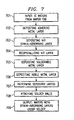
- FIG. 7 shows a block diagram of the preferred wafer-level process flow of manufacturing the NiTi layer, emphasizing the following major steps:
- the invention can be applied to IC bond pad metallizations other than copper, which are difficult or impossible to contact by conventional tin or solder techniques, such as alloys of refractory metals and noble metals.
- the invention can be extended to batch processing, further reducing fabrication costs.
- the invention provides freedom to the composition of the NiTi alloy, the thickness of the alloy layer, and the recrystallization temperatures and times. It is therefore intended that the appended claims encompass any such modifications or embodiments.
Landscapes
- Wire Bonding (AREA)
- Internal Circuitry In Semiconductor Integrated Circuit Devices (AREA)
- Electrodes Of Semiconductors (AREA)
Abstract
Description
- a lower superelastic plateau stress for the eutectic solder alloy of 18 to 30 MPa while below 0 to 20 °C, and
- a lower superelastic plateau stress for the lead-free solder alloy of 26.5 to 40 MPa while below 15 °C.
- Step 701: Input: IC wafer from the wafer fab. The wafer has a protective overcoat and a plurality of windows in this overcoat to expose the aluminum or copper interconnecting chip metallization.
- Step 702: Depositing by sputtering a Ti (or other refractory metal) layer operable to contact the chip metallization and to adhere to the chip protective overcoat;
- Step 703: Depositing by DC (160 W/in2) or RF sputtering a NiTi alloy of 55.5 ± 0.5 weight% Ni and 44.5 ± 0.5 weight% Ti; after about 1.0 hr at ambient temperature, the layer is in the thickness range of 4.0 ± 1.5 µm;
- Step 704: Recrystallizing the alloy layer at 450 to 600 °C for 4 to 6 min, creating a martensite crystalline structure having a Lower Superelastic Plateau Stress which is lower than the yield stress of the solder attachment, and is operable in reversible phase transitions under thermomechanical stress, whereby mechanical strain is absorbed by the alloy layer;
- Step 705: Depositing by sputtering, or by sputtering and electro- or electroless plating, a Ni layer of 0.3 to 0.7 µm thickness to act as a solderable surface and as a diffusion barrier;
- Step 706: Depositing by sputtering or by electroplating a layer of palladium, about 0.02 µm thick, or 0.003 to 0.005 µm gold, to preserve the solderability of nickel;
- Step 707: Patterning the deposited layers by acid etching to provide solder attach sites;
- Step 708: Attaching solder "balls".
- Step 709: Output: IC wafers with strain-absorbing layers under solder interconnections.
will be apparent to persons skilled in the art upon reference to the description. As an example, the invention can be applied to IC bond pad metallizations other than copper, which are difficult or impossible to contact by conventional tin or solder techniques, such as alloys of refractory metals and noble metals. As another example, the invention can be extended to batch processing, further reducing fabrication costs. As another example, the invention provides freedom to the composition of the NiTi alloy, the thickness of the alloy layer, and the recrystallization temperatures and times. It is therefore intended that the appended claims encompass any such modifications or embodiments.
Claims (10)
- An integrated circuit chip having a plurality of contact pads to be connected by reflow attachment to outside parts, comprising:a deposited layer of nickel/titanium alloy on each of said pads, said alloy having a composition and crystalline structure operable in reversible phase transitions under thermomechanical stress, whereby mechanical strain is absorbed by said alloy layer; anda layer of solderable metal on said alloy, operable as diffusion barrier after said reflow attachment.
- The chip according to Claim 1 wherein said alloy has 55.5 ± 0.5 weight% nickel and 44.5 ± 0.5 weight% titanium.
- The chip according to Claims 1 or 2 wherein said alloy layer has a thickness in the range from about 0.3 to 6.0 µm.
- The chip according to any of Claims 1, 2 or 3 wherein said crystalline structure is martensite, having a Lower Superelastic Plateau Stress which is lower than the yield stress of said reflow attachment to outside parts.
- The chip according to any of Claims 1 to 4 wherein said reversible phase transitions are operable in the temperature range from -40 to +125 °C.
- The chip according to Claim 1 wherein said solderable metal layer is made of nickel and has a thickness in the range from about 0.3 to 0.7 µm.
- A semiconductor device assembly including a metallurgical interconnection attaching an electronic device having first coefficient of thermal expansion to an outside body having second coefficient of thermal expansion, comprising:an electronic device having a plurality of contact pads;each of said contact pads including a layer of nickel/titanium alloy covered by a solderable nickel barrier layer;a solder bump attached to said solderable layer of each contact pad;said outside body having a plurality of terminal pads located in positions corresponding to said device contact pads;said device attached to said outside body so that said contact pads are aligned with said corresponding terminal pads, whereby a plurality of metallurgical interconnections are formed operable to absorb, in said nickel/titanium layer, strain caused by thermomechanical stress due to the difference between said first and second coefficients of thermal expansion.
- The chip according to Claim 7 wherein said alloy has 55.5 ± 0.5 weight% nickel and 44.5 ± 0.5 weight% titanium.
- A method of fabricating integrated circuit chips having a plurality of contact pads to be connected by reflow attachment to outside parts, comprising the steps of:depositing a layer of nickel/titanium alloy composed of 55.5 ± 0.5 weight% nickel and 44.5 ± 0.5 weight% titanium on said contact pads;depositing a layer of solderable metal on said alloy.
- The method of Claim 9, further comprising the step of recrystallizing said alloy at a temperature in the range of 450 to 600 °C.
Applications Claiming Priority (4)
| Application Number | Priority Date | Filing Date | Title |
|---|---|---|---|
| US38142002P | 2002-05-17 | 2002-05-17 | |
| US381420P | 2002-05-17 | ||
| US10/205,455 US7095121B2 (en) | 2002-05-17 | 2002-07-25 | Metallic strain-absorbing layer for improved fatigue resistance of solder-attached devices |
| US205455 | 2002-07-25 |
Publications (2)
| Publication Number | Publication Date |
|---|---|
| EP1365449A2 true EP1365449A2 (en) | 2003-11-26 |
| EP1365449A3 EP1365449A3 (en) | 2004-01-21 |
Family
ID=29406394
Family Applications (1)
| Application Number | Title | Priority Date | Filing Date |
|---|---|---|---|
| EP03101352A Withdrawn EP1365449A3 (en) | 2002-05-17 | 2003-05-14 | Metallic strain-absorbing layer for improved fatigue resistance of solder-attached devices |
Country Status (3)
| Country | Link |
|---|---|
| US (2) | US7095121B2 (en) |
| EP (1) | EP1365449A3 (en) |
| JP (1) | JP2004006872A (en) |
Cited By (3)
| Publication number | Priority date | Publication date | Assignee | Title |
|---|---|---|---|---|
| DE102006016090A1 (en) * | 2006-04-04 | 2007-10-18 | Albert-Ludwigs-Universität Freiburg | Solder material producing method for e.g. flip-chip-connection between substrate and semiconductor, involves converting surface of passivation layer into finely nubby or slightly wettable surface by surface treatment |
| WO2009016531A3 (en) * | 2007-07-30 | 2009-04-02 | Nxp Bv | Reduced bottom roughness of stress buffering element of a semiconductor component |
| WO2009068373A1 (en) * | 2007-11-29 | 2009-06-04 | International Business Machines Corporation | Underbump metallurgy employing sputter-deposited nickel titanium alloy |
Families Citing this family (33)
| Publication number | Priority date | Publication date | Assignee | Title |
|---|---|---|---|---|
| US6867503B2 (en) * | 2003-05-07 | 2005-03-15 | Texas Instruments Incorporated | Controlling interdiffusion rates in metal interconnection structures |
| US7193326B2 (en) * | 2003-06-23 | 2007-03-20 | Denso Corporation | Mold type semiconductor device |
| TWI239620B (en) * | 2003-09-05 | 2005-09-11 | Advanced Semiconductor Eng | Method for forming ball pads of ball grid array package substrate |
| US7064446B2 (en) * | 2004-03-29 | 2006-06-20 | Intel Corporation | Under bump metallization layer to enable use of high tin content solder bumps |
| US7109587B1 (en) * | 2004-05-25 | 2006-09-19 | National Semiconductor Corporation | Apparatus and method for enhanced thermal conductivity packages for high powered semiconductor devices |
| US20050275096A1 (en) * | 2004-06-11 | 2005-12-15 | Kejun Zeng | Pre-doped reflow interconnections for copper pads |
| US7446399B1 (en) * | 2004-08-04 | 2008-11-04 | Altera Corporation | Pad structures to improve board-level reliability of solder-on-pad BGA structures |
| US7223695B2 (en) * | 2004-09-30 | 2007-05-29 | Intel Corporation | Methods to deposit metal alloy barrier layers |
| DE102005051857A1 (en) * | 2005-05-25 | 2007-02-22 | Fraunhofer-Gesellschaft zur Förderung der angewandten Forschung e.V. | UBM-PAD, solder contact and method of making a solder joint |
| US20070085220A1 (en) * | 2005-10-19 | 2007-04-19 | Hortaleza Edgardo R | Re-enforced ball-grid array packages for semiconductor products |
| KR100718169B1 (en) * | 2006-01-12 | 2007-05-15 | 한국과학기술원 | Joining method of nickel surface-treated electronic parts and electroless nickel surface-treated electronic parts |
| DE602007013181D1 (en) * | 2006-01-24 | 2011-04-28 | Nxp Bv | VOLTAGE BUFFER HOUSING FOR A SEMICONDUCTOR COMPONENT |
| US7923836B2 (en) * | 2006-07-21 | 2011-04-12 | International Business Machines Corporation | BLM structure for application to copper pad |
| US20080157910A1 (en) * | 2006-12-29 | 2008-07-03 | Park Chang-Min | Amorphous soft magnetic layer for on-die inductively coupled wires |
| SG148056A1 (en) | 2007-05-17 | 2008-12-31 | Micron Technology Inc | Integrated circuit packages, methods of forming integrated circuit packages, and methods of assembling intgrated circuit packages |
| US7982137B2 (en) * | 2007-06-27 | 2011-07-19 | Hamilton Sundstrand Corporation | Circuit board with an attached die and intermediate interposer |
| US7763965B2 (en) * | 2007-09-25 | 2010-07-27 | International Business Machines Corporation | Stress relief structures for silicon interposers |
| US20090108443A1 (en) * | 2007-10-30 | 2009-04-30 | Monolithic Power Systems, Inc. | Flip-Chip Interconnect Structure |
| US8809182B2 (en) | 2008-05-01 | 2014-08-19 | International Business Machines Corporation | Pad cushion structure and method of fabrication for Pb-free C4 integrated circuit chip joining |
| JP5062022B2 (en) * | 2008-05-08 | 2012-10-31 | 富士通株式会社 | Electronic component equipment |
| US7888259B2 (en) * | 2008-08-19 | 2011-02-15 | Ati Technologies Ulc | Integrated circuit package employing predetermined three-dimensional solder pad surface and method for making same |
| JP4888473B2 (en) * | 2008-11-20 | 2012-02-29 | ソニー株式会社 | Mounting board |
| WO2010082342A1 (en) * | 2009-01-16 | 2010-07-22 | トヨタ自動車株式会社 | Semiconductor device, process for fabricating semiconductor device, apparatus for fabricating semiconductor device, and method for evaluating semiconductor device |
| US20110006409A1 (en) * | 2009-07-13 | 2011-01-13 | Gruenhagen Michael D | Nickel-titanum contact layers in semiconductor devices |
| US20110031596A1 (en) * | 2009-08-05 | 2011-02-10 | Gruenhagen Mike D | Nickel-titanum soldering layers in semiconductor devices |
| JP2011165862A (en) * | 2010-02-09 | 2011-08-25 | Sony Corp | Semiconductor device, chip-on-chip mounting structure, method for manufacturing semiconductor device, and method for forming chip-on-chip mounting structure |
| TWI419284B (en) * | 2010-05-26 | 2013-12-11 | 南茂科技股份有限公司 | Bulk structure of wafer and manufacturing method of bump structure |
| TW201208007A (en) * | 2010-08-02 | 2012-02-16 | Advanced Semiconductor Eng | Semiconductor package |
| US8426971B2 (en) * | 2010-08-27 | 2013-04-23 | Diodes FabTech, Inc. | Top tri-metal system for silicon power semiconductor devices |
| TWI490994B (en) * | 2012-09-03 | 2015-07-01 | 矽品精密工業股份有限公司 | Connection structure in a semiconductor package |
| US9312607B2 (en) | 2013-02-12 | 2016-04-12 | Raytheon Company | Load spreading interposer |
| CN108281404A (en) * | 2015-04-30 | 2018-07-13 | 华为技术有限公司 | A kind of integrated circuit die and manufacturing method |
| US20220312591A1 (en) * | 2021-03-26 | 2022-09-29 | Juniper Networks, Inc. | Substrate with conductive pads and conductive layers |
Family Cites Families (9)
| Publication number | Priority date | Publication date | Assignee | Title |
|---|---|---|---|---|
| JPS6481264A (en) | 1987-09-22 | 1989-03-27 | Fujitsu Ltd | Semiconductor device |
| US4950623A (en) * | 1988-08-02 | 1990-08-21 | Microelectronics Center Of North Carolina | Method of building solder bumps |
| FR2736569B1 (en) | 1995-07-13 | 1997-08-08 | Thomson Csf | CONNECTION DEVICE AND CONNECTION METHOD |
| JPH09129647A (en) | 1995-10-27 | 1997-05-16 | Toshiba Corp | Semiconductor element |
| US6255723B1 (en) | 1997-10-27 | 2001-07-03 | Tessera, Inc. | Layered lead structures |
| FR2772657B1 (en) * | 1997-12-23 | 2000-03-03 | Thomson Csf | PROCEDURE FOR PRODUCING BRAZING PASTE AND WELDING JOINT OBTAINED |
| US6544880B1 (en) * | 1999-06-14 | 2003-04-08 | Micron Technology, Inc. | Method of improving copper interconnects of semiconductor devices for bonding |
| JP2001024021A (en) | 1999-07-09 | 2001-01-26 | Hitachi Ltd | Semiconductor device and manufacturing method thereof |
| US6489229B1 (en) * | 2001-09-07 | 2002-12-03 | Motorola, Inc. | Method of forming a semiconductor device having conductive bumps without using gold |
-
2002
- 2002-07-25 US US10/205,455 patent/US7095121B2/en not_active Expired - Lifetime
-
2003
- 2003-05-14 EP EP03101352A patent/EP1365449A3/en not_active Withdrawn
- 2003-05-16 JP JP2003138890A patent/JP2004006872A/en not_active Abandoned
-
2004
- 2004-03-01 US US10/789,643 patent/US7012018B2/en not_active Expired - Lifetime
Cited By (5)
| Publication number | Priority date | Publication date | Assignee | Title |
|---|---|---|---|---|
| DE102006016090A1 (en) * | 2006-04-04 | 2007-10-18 | Albert-Ludwigs-Universität Freiburg | Solder material producing method for e.g. flip-chip-connection between substrate and semiconductor, involves converting surface of passivation layer into finely nubby or slightly wettable surface by surface treatment |
| DE102006016090B4 (en) * | 2006-04-04 | 2011-12-08 | Albert-Ludwigs-Universität Freiburg | Method for producing a plurality of solder deposits on a substrate |
| WO2009016531A3 (en) * | 2007-07-30 | 2009-04-02 | Nxp Bv | Reduced bottom roughness of stress buffering element of a semiconductor component |
| US8350385B2 (en) | 2007-07-30 | 2013-01-08 | Nxp B.V. | Reduced bottom roughness of stress buffering element of a semiconductor component |
| WO2009068373A1 (en) * | 2007-11-29 | 2009-06-04 | International Business Machines Corporation | Underbump metallurgy employing sputter-deposited nickel titanium alloy |
Also Published As
| Publication number | Publication date |
|---|---|
| US20030214037A1 (en) | 2003-11-20 |
| US20040164421A1 (en) | 2004-08-26 |
| EP1365449A3 (en) | 2004-01-21 |
| JP2004006872A (en) | 2004-01-08 |
| US7095121B2 (en) | 2006-08-22 |
| US7012018B2 (en) | 2006-03-14 |
Similar Documents
| Publication | Publication Date | Title |
|---|---|---|
| US7012018B2 (en) | Metallic strain-absorbing layer for improved fatigue resistance of solder-attached devices | |
| Frear et al. | Pb-free solders for flip-chip interconnects | |
| US6696757B2 (en) | Contact structure for reliable metallic interconnection | |
| CN100421861C (en) | solder | |
| JP4972503B2 (en) | Semiconductor power module | |
| JP3489811B2 (en) | Method for manufacturing semiconductor device | |
| JP4731495B2 (en) | Semiconductor device | |
| US20050275096A1 (en) | Pre-doped reflow interconnections for copper pads | |
| US7884009B2 (en) | Semiconductor device with an improved solder joint | |
| US20090085228A1 (en) | Die warpage control | |
| JPH07302797A (en) | Semiconductor device and method of manufacturing and using the same | |
| JP4036786B2 (en) | Electronic component mounting method | |
| CN1983542A (en) | Method for manufacturing electronic device | |
| JP2002301588A (en) | Solder foil, semiconductor device and electronic device | |
| KR101279291B1 (en) | Lead-free solder joint structure and solder ball | |
| Tu et al. | Effect of intermetallic compounds on vibration fatigue of/spl mu/BGA solder joint | |
| JP2002305213A (en) | Solder foil, semiconductor device and electronic device | |
| US7267861B2 (en) | Solder joints for copper metallization having reduced interfacial voids | |
| US20050029675A1 (en) | Tin/indium lead-free solders for low stress chip attachment | |
| US20080083993A1 (en) | Gold-Tin Solder Joints Having Reduced Embrittlement | |
| US6867503B2 (en) | Controlling interdiffusion rates in metal interconnection structures | |
| JP2697116B2 (en) | Indium solder joint structure | |
| US8268716B2 (en) | Creation of lead-free solder joint with intermetallics | |
| Uchida et al. | Low-stress interconnection for flip chip BGA employing lead-free solder bump | |
| JP2001156095A (en) | Electrode, semiconductor device and manufacturing method |
Legal Events
| Date | Code | Title | Description |
|---|---|---|---|
| PUAI | Public reference made under article 153(3) epc to a published international application that has entered the european phase |
Free format text: ORIGINAL CODE: 0009012 |
|
| AK | Designated contracting states |
Kind code of ref document: A2 Designated state(s): AT BE BG CH CY CZ DE DK EE ES FI FR GB GR HU IE IT LI LU MC NL PT RO SE SI SK TR |
|
| AX | Request for extension of the european patent |
Extension state: AL LT LV MK |
|
| PUAL | Search report despatched |
Free format text: ORIGINAL CODE: 0009013 |
|
| AK | Designated contracting states |
Kind code of ref document: A3 Designated state(s): AT BE BG CH CY CZ DE DK EE ES FI FR GB GR HU IE IT LI LU MC NL PT RO SE SI SK TR |
|
| AX | Request for extension of the european patent |
Extension state: AL LT LV MK |
|
| AKX | Designation fees paid | ||
| REG | Reference to a national code |
Ref country code: DE Ref legal event code: 8566 |
|
| STAA | Information on the status of an ep patent application or granted ep patent |
Free format text: STATUS: THE APPLICATION IS DEEMED TO BE WITHDRAWN |
|
| 18D | Application deemed to be withdrawn |
Effective date: 20040722 |