EP1365308A2 - Method and apparatus for minimizing differential power attacks on processors - Google Patents
Method and apparatus for minimizing differential power attacks on processors Download PDFInfo
- Publication number
- EP1365308A2 EP1365308A2 EP03018048A EP03018048A EP1365308A2 EP 1365308 A2 EP1365308 A2 EP 1365308A2 EP 03018048 A EP03018048 A EP 03018048A EP 03018048 A EP03018048 A EP 03018048A EP 1365308 A2 EP1365308 A2 EP 1365308A2
- Authority
- EP
- European Patent Office
- Prior art keywords
- value
- secret value
- parts
- components
- combined
- Prior art date
- Legal status (The legal status is an assumption and is not a legal conclusion. Google has not performed a legal analysis and makes no representation as to the accuracy of the status listed.)
- Granted
Links
Images


Classifications
-
- H—ELECTRICITY
- H04—ELECTRIC COMMUNICATION TECHNIQUE
- H04L—TRANSMISSION OF DIGITAL INFORMATION, e.g. TELEGRAPHIC COMMUNICATION
- H04L9/00—Cryptographic mechanisms or cryptographic arrangements for secret or secure communications; Network security protocols
- H04L9/002—Countermeasures against attacks on cryptographic mechanisms
- H04L9/003—Countermeasures against attacks on cryptographic mechanisms for power analysis, e.g. differential power analysis [DPA] or simple power analysis [SPA]
-
- G—PHYSICS
- G06—COMPUTING OR CALCULATING; COUNTING
- G06F—ELECTRIC DIGITAL DATA PROCESSING
- G06F21/00—Security arrangements for protecting computers, components thereof, programs or data against unauthorised activity
- G06F21/70—Protecting specific internal or peripheral components, in which the protection of a component leads to protection of the entire computer
- G06F21/71—Protecting specific internal or peripheral components, in which the protection of a component leads to protection of the entire computer to assure secure computing or processing of information
- G06F21/75—Protecting specific internal or peripheral components, in which the protection of a component leads to protection of the entire computer to assure secure computing or processing of information by inhibiting the analysis of circuitry or operation
- G06F21/755—Protecting specific internal or peripheral components, in which the protection of a component leads to protection of the entire computer to assure secure computing or processing of information by inhibiting the analysis of circuitry or operation with measures against power attack
-
- G—PHYSICS
- G06—COMPUTING OR CALCULATING; COUNTING
- G06F—ELECTRIC DIGITAL DATA PROCESSING
- G06F16/00—Information retrieval; Database structures therefor; File system structures therefor
- G06F16/10—File systems; File servers
- G06F16/17—Details of further file system functions
- G06F16/176—Support for shared access to files; File sharing support
-
- G—PHYSICS
- G06—COMPUTING OR CALCULATING; COUNTING
- G06F—ELECTRIC DIGITAL DATA PROCESSING
- G06F7/00—Methods or arrangements for processing data by operating upon the order or content of the data handled
- G06F7/60—Methods or arrangements for performing computations using a digital non-denominational number representation, i.e. number representation without radix; Computing devices using combinations of denominational and non-denominational quantity representations, e.g. using difunction pulse trains, STEELE computers, phase computers
- G06F7/72—Methods or arrangements for performing computations using a digital non-denominational number representation, i.e. number representation without radix; Computing devices using combinations of denominational and non-denominational quantity representations, e.g. using difunction pulse trains, STEELE computers, phase computers using residue arithmetic
-
- G—PHYSICS
- G06—COMPUTING OR CALCULATING; COUNTING
- G06F—ELECTRIC DIGITAL DATA PROCESSING
- G06F9/00—Arrangements for program control, e.g. control units
- G06F9/06—Arrangements for program control, e.g. control units using stored programs, i.e. using an internal store of processing equipment to receive or retain programs
- G06F9/30—Arrangements for executing machine instructions, e.g. instruction decode
- G06F9/30003—Arrangements for executing specific machine instructions
- G06F9/3005—Arrangements for executing specific machine instructions to perform operations for flow control
- G06F9/30058—Conditional branch instructions
-
- G—PHYSICS
- G06—COMPUTING OR CALCULATING; COUNTING
- G06K—GRAPHICAL DATA READING; PRESENTATION OF DATA; RECORD CARRIERS; HANDLING RECORD CARRIERS
- G06K19/00—Record carriers for use with machines and with at least a part designed to carry digital markings
- G06K19/06—Record carriers for use with machines and with at least a part designed to carry digital markings characterised by the kind of the digital marking, e.g. shape, nature, code
- G06K19/067—Record carriers with conductive marks, printed circuits or semiconductor circuit elements, e.g. credit or identity cards also with resonating or responding marks without active components
- G06K19/07—Record carriers with conductive marks, printed circuits or semiconductor circuit elements, e.g. credit or identity cards also with resonating or responding marks without active components with integrated circuit chips
- G06K19/073—Special arrangements for circuits, e.g. for protecting identification code in memory
- G06K19/07309—Means for preventing undesired reading or writing from or onto record carriers
- G06K19/07363—Means for preventing undesired reading or writing from or onto record carriers by preventing analysis of the circuit, e.g. dynamic or static power analysis or current analysis
-
- G—PHYSICS
- G06—COMPUTING OR CALCULATING; COUNTING
- G06F—ELECTRIC DIGITAL DATA PROCESSING
- G06F2207/00—Indexing scheme relating to methods or arrangements for processing data by operating upon the order or content of the data handled
- G06F2207/72—Indexing scheme relating to groups G06F7/72 - G06F7/729
- G06F2207/7219—Countermeasures against side channel or fault attacks
-
- G—PHYSICS
- G06—COMPUTING OR CALCULATING; COUNTING
- G06F—ELECTRIC DIGITAL DATA PROCESSING
- G06F2207/00—Indexing scheme relating to methods or arrangements for processing data by operating upon the order or content of the data handled
- G06F2207/72—Indexing scheme relating to groups G06F7/72 - G06F7/729
- G06F2207/7219—Countermeasures against side channel or fault attacks
- G06F2207/7223—Randomisation as countermeasure against side channel attacks
- G06F2207/7233—Masking, e.g. (A**e)+r mod n
- G06F2207/7242—Exponent masking, i.e. key masking, e.g. A**(e+r) mod n; (k+r).P
-
- H—ELECTRICITY
- H04—ELECTRIC COMMUNICATION TECHNIQUE
- H04L—TRANSMISSION OF DIGITAL INFORMATION, e.g. TELEGRAPHIC COMMUNICATION
- H04L2209/00—Additional information or applications relating to cryptographic mechanisms or cryptographic arrangements for secret or secure communication H04L9/00
- H04L2209/04—Masking or blinding
- H04L2209/046—Masking or blinding of operations, operands or results of the operations
-
- Y—GENERAL TAGGING OF NEW TECHNOLOGICAL DEVELOPMENTS; GENERAL TAGGING OF CROSS-SECTIONAL TECHNOLOGIES SPANNING OVER SEVERAL SECTIONS OF THE IPC; TECHNICAL SUBJECTS COVERED BY FORMER USPC CROSS-REFERENCE ART COLLECTIONS [XRACs] AND DIGESTS
- Y02—TECHNOLOGIES OR APPLICATIONS FOR MITIGATION OR ADAPTATION AGAINST CLIMATE CHANGE
- Y02D—CLIMATE CHANGE MITIGATION TECHNOLOGIES IN INFORMATION AND COMMUNICATION TECHNOLOGIES [ICT], I.E. INFORMATION AND COMMUNICATION TECHNOLOGIES AIMING AT THE REDUCTION OF THEIR OWN ENERGY USE
- Y02D10/00—Energy efficient computing, e.g. low power processors, power management or thermal management
Definitions
- This invention relates to cryptographic systems and in particular to a method and apparatus for minimizing successful power analysis attacks on processors.
- Cryptographic systems generally owe their security to the fact that a particular piece of information is kept secret, without which it is almost impossible to break the scheme.
- This secret information must generally be stored within a secure boundary, making it difficult for an attacker to get at it directly however, various schemes or attacks have been attempted in order to obtain the secret information.
- portable cryptographic tokens including smart cards and the like.
- simple power analysis differential power analysis
- higher order differential power analysis and other related techniques.
- These technically sophisticated and extremely powerful analysis tools can be used by an attacker to extract secret keys from cryptographic devices. It has been shown that these attacks can be mounted quickly and can be implemented using readily available hardware. The amount of time required for these attacks depends on the type of attack and varies somewhat by device. For example it has been shown that a simple power attack (SPA) typically take a few seconds per card, while the differential power attacks (DPA) can take several hours.
- SPA simple power attack
- DPA differential power attacks
- Encryption operations are performed in a processor operating in a sequential manner by performing a sequence of fundamental operations, each of which generates a distinct timing pattern. Laborious but careful analysis of end-to-end power waveforms can decompose the order of these fundamental operations performed on each bit of a secret key and thus be, analyzed to find the entire secret key, compromising the system.
- the differential power analysis attack is a more powerful attack than the SPA and is much more difficult to prevent.
- the DPA uses statistical analysis and error correction techniques to extract information which may be correlated to secret keys, while the SPA attacks use primarily visual inspection to identify relevant power fluctuations.
- the DPA attack is performed in two steps. The first step is recording data that reflects the change in power consumed by the card during execution of cryptographic routines. In the second step, the collected data is statistically analyzed to extract information correlated to secret keys. A detailed analysis of these attacks is described in the paper entitled "Introduction to Differential Power Analysis and Related Attacks" by Paul Kocher et al.
- branches in program flow are particularly vulnerable to power analysis measurements.
- V some distinguishing value
- one of two branches of the program is executed.
- V is compared with a threshold value and a jump to one of two locations is executed as a result of the comparison.
- the flow diagram indicates a scenario where a distinguishing value V varies within a range and the condition is whether a threshold value TH is crossed by the distinguishing value V or not.
- the threshold TH is a random number between an upper limit and a lower limit VMAX and VMIN, respectively.
- a method of masking a conditional jump operation in a processor wherein program execution jumps to one of two branches dependent on a first or second condition of a distinguishing value V relative to a reference value and wherein the reference is bounded by an upper limit Vmax and a lower limit Vmin, the method comprising the steps of:
- the distinguishing value is combined with a random value, thereby adding a random number of instructions on every condition evaluation.
- FIG 2 a schematic diagram of a method for masking conditional jump statements in a computer program, according to an embodiment of the present invention, is shown generally by numeral 50.
- a distinguishing value V varies within a known range and the condition is whether a threshold value TH is crossed by the distinguishing value V or not.
- the threshold TH is a random number in the known range having an upper limit and a lower limit VMAX and VMIN, respectively.
- the method comprises the steps of identifying a location for a conditional jump operation, and inserting at the location a call 52 to a subroutine 54, the subroutine 54 including instructions for changing the return address of the subroutine to one of two program branches to execute branch statements1 or branch statements2 in response to the result of a comparison of the distinguishing value V to the threshold value.
- the subroutine is identified as IRRITATE_1 (54) and includes code blocks identified as b, c, d and e.
- the code block c includes a first and second sections 56 and 58, respectively.
- the start address of the second section 58 is predetermined and is indicated by the value KNOWN_DISPLACEMENT.
- the start address of the first section 56 is then determined by the difference between KNOWN_DISPLACEMENT and the upper limit of the distinguishing value V.
- the first section 56 consists of a series of unconditional jumps to an address L1 and the second section 58 consists of a series of unconditional jumps to an address L2.
- the locations L1 and L2 contain code for returning program flow to execute statements1 and statements2 respectively.
- the code block b included in the subroutine IRRITATE_1 includes code for computing a difference between the KNOWN_DISPLACEMENT address and the THRESHOLD. The resulting address is then added to the distinguishing value V to derive a target address location in one of the sections 56 or 58.
- V is preserved while calling the subroutine, which in turn does not contain any conditional jumps.
- this subroutine we change the return address of the subroutine (which resides on the stack) depending on whether V is below or above TH in such a way that, after returning from the subroutine, the program will continue execution in the desired branch.
- extended addressing An addressing mode known as extended addressing is used to determine the target address.
- extended addressing the address at which the execution of the program has to continue is computed as the sum of the content of two registers.
- JMP @A+DPTR in the assembly language of the Intel 8051 family means that the address at which the program execution has to continue is computed by adding the content of the accumulator A and the data pointer DPTR.
- Other processors may support similar mechanisms for addressing.
- the code fragments shown in figure 2 illustrate the method. To refer to lines of these code fragments we use labels consisting of a letter and a number. Thus to implement this method we have to specify:
- the code fragments shown in figure 2 will be discussed below.
- the code fragments may be located within a loop, which sequentially changes the value of V in a given range for iterations of the loop.
- V may the value of the loop counter.
- the THRESHOLD value is a random value within the known range of Vmin and Vmax.
- the distinguishing value V is stored in the accumulator of the processor and the subroutine IRRITATE_1 is called at line a2.
- the return address from this subroutine will be line a3, which is automatically stored on the stack by the processor.
- KNOWN_DISPLACEMENT in line b1 is a constant value that specifies the beginning location of the second section 58 and indicates the address of line c9.
- KNOWN_DISPLACEMENT-Vmax is the address of line c1, the beginning location of the first section 56.
- Block b the value of KNOWN_DISPLACEMENT is stored in a register at line b1
- the register is updated with the difference of KNOWN_DISPLACEMENT and THRESHOLD. This difference is moved to in DPTR at line b3.
- the labels L1 and L2 point to addresses located at lines c17 and c21 respectively.
- the return address of the subroutine IRRITATE_1 is retrieved and changed such that the program counter will point to line a3 after returning from the subroutine.
- the return address of the subroutine IRRITATE_1 is also retrieved and changed such that the program counter will point to line a4 after returning from the subroutine.
- jump instructions in lines a3 and a4 which redirect program flow to statements1 and statements2 respectively, should be placed at addresses with the same number of 1's in their binary representation. This would result in homogenous power consumption on the address bus while addressing these two different locations.
- the same precaution applies to the lines d1 and e1, the beginning location of statements1 and statements2 respectively.
- special attention should be paid to the choice of values of THRESHOLD and KNOWN_DISPLCEMENT to avoid changes in flags in the processors status word while the SUB instruction is being executed.
- a second embodiment of the present invention is shown generally by numeral 100.
- This embodiment also utilizes extended addressing as described earlier. Again, assembly language of the Intel 8051 family of processors is used to illustrate the method. For clarity the symbols op1 through op7 are used to represent program instructions.
- the distinguishing value V is one of two distinct values Vmax and Vmin, rather than a range of values. Thus, the condition in this case is when the distinguishing value V is one or the other of the distinct values Vmax or Vmin.
- the subroutine including instructions for changing the return address of the subroutine to one of two program branches to execute branch statements 1 or branch statements2 in response to the distinguishing value V being one of the two distinct values Vmax or Vmin.
- code block f the location of the conditional jump that is replaced is identified by code block f.
- the subroutine is identified as IRRITATE_2 (102) and includes code blocks identified as blocks g and h.
- the code block h also includes first and second sections 106 and 108, respectively. Each of the sections contain a series of dummy operations op1 indicated at lines h1 through h7 and at lines h12 through h18. Each of the sections is terminated by a sequence of instructions for retrieving the return address of the subroutine IRRITATE_2 and changing it such that the program counter will point to line f4 or f5 after returning from the subroutine.
- the lines f4 and f4 include jumps to one of the two branches indicated as block i and block j which contain statements1 and statements2 respectively.
- the target destination address is comprised of two components, namely the distinguishing value V or a value derived from V and a random number MASKED_RANDOM, that are added at line g1.
- the beginning address of the first and second sections are chosen such that this target address is either in the range of lines h1 through h8 or h12 through h19. Since, the second component of the target address is a random number, a random number of dummy operations will be executed before the return address of the subroutine IRRITATE_2 is computed at lines h8 to h10 (or h19 to h21).
- the ADD values at lines h9 and h20 may be chosen to have the same hamming weight(number of 1's), with appropriate number of NOP instructions added to block f.
- the jump instructions at lines f4 and f5 may be placed at addresses with the same number of one's. Additional JMP instructions may also be inserted between the lines h1 and h8 with a destination in the same segment.
- This embodiment thus uses unconditional jumps instead of conditional jumps and adds a random number of dummy operations to the code.
- the former property is a countermeasure against SPA and the latter makes DPA attacks more difficult.
- this embodiment adds a random mask or noise to the program execution path since the jump to a random address within a segment causes program execution of a random number of operations before one of the branches is executed. Therefore each time one of the branches is executed, the number of operations performed by the processor varies randomly making DPA attacks more difficult.
- an embodiment of a method for masking a private key or secret used in a cryptographic operation is shown generally by numeral 200.
- the method comprises the steps of dividing the key into a plurality of parts and combining with each part a random value modulo n (where n is the number of points on the elliptic curve) to derive a new part such that the new parts are combined to be equivalent to the original private key value and utilizing each of the individual parts in the operation.
- the cryptographic processor is initialized with the public key or secret value d.
- the secret key d is normally combined with the point P to derive dP.
- d b 10 + b 20 .
- b 1 and b 2 are stored instead of d.
- the d value may also be stored if so desired, however in the case of a smart card where memory is limited this may not be desirable.
- R' (sP-eQ) which should correspond to R. If the computed values correspond then the signature is verified.
- Both the secret keys in the above example may be masked using the method of the present invention.
Landscapes
- Engineering & Computer Science (AREA)
- Theoretical Computer Science (AREA)
- Physics & Mathematics (AREA)
- General Physics & Mathematics (AREA)
- General Engineering & Computer Science (AREA)
- Computer Hardware Design (AREA)
- Software Systems (AREA)
- Computer Security & Cryptography (AREA)
- Mathematical Physics (AREA)
- Mathematical Analysis (AREA)
- Computational Mathematics (AREA)
- Mathematical Optimization (AREA)
- Pure & Applied Mathematics (AREA)
- Computing Systems (AREA)
- Computer Networks & Wireless Communication (AREA)
- Signal Processing (AREA)
- Microelectronics & Electronic Packaging (AREA)
- Data Mining & Analysis (AREA)
- Databases & Information Systems (AREA)
- Storage Device Security (AREA)
- Debugging And Monitoring (AREA)
- Executing Machine-Instructions (AREA)
Abstract
Description
- This invention relates to cryptographic systems and in particular to a method and apparatus for minimizing successful power analysis attacks on processors.
- Cryptographic systems generally owe their security to the fact that a particular piece of information is kept secret, without which it is almost impossible to break the scheme. This secret information must generally be stored within a secure boundary, making it difficult for an attacker to get at it directly however, various schemes or attacks have been attempted in order to obtain the secret information. Of particular risk are portable cryptographic tokens, including smart cards and the like. Of the more recent attacks performed on these particularly vulnerable devices are simple power analysis, differential power analysis, higher order differential power analysis and other related techniques. These technically sophisticated and extremely powerful analysis tools can be used by an attacker to extract secret keys from cryptographic devices. It has been shown that these attacks can be mounted quickly and can be implemented using readily available hardware. The amount of time required for these attacks depends on the type of attack and varies somewhat by device. For example it has been shown that a simple power attack (SPA) typically take a few seconds per card, while the differential power attacks (DPA) can take several hours.
- Encryption operations are performed in a processor operating in a sequential manner by performing a sequence of fundamental operations, each of which generates a distinct timing pattern. Laborious but careful analysis of end-to-end power waveforms can decompose the order of these fundamental operations performed on each bit of a secret key and thus be, analyzed to find the entire secret key, compromising the system.
- In the simple power analysis (SPA) attacks on smart cards and other secure tokens, an attacker directly measures the token's power consumption changes over time. The amount of power consumed varies depending on the executed microprocessor instructions. A large calculation such as elliptic curve (EC) additions in a loop and DES rounds, etc, may be identified, since the operations performed with a microprocessor vary significantly during different parts of these operations. By sampling the current and voltage at a higher rate, i.e., higher resolution, individual instructions can be differentiated.
- The differential power analysis attack (DPA) is a more powerful attack than the SPA and is much more difficult to prevent. Primarily, the DPA uses statistical analysis and error correction techniques to extract information which may be correlated to secret keys, while the SPA attacks use primarily visual inspection to identify relevant power fluctuations. The DPA attack is performed in two steps. The first step is recording data that reflects the change in power consumed by the card during execution of cryptographic routines. In the second step, the collected data is statistically analyzed to extract information correlated to secret keys. A detailed analysis of these attacks is described in the paper entitled "Introduction to Differential Power Analysis and Related Attacks" by Paul Kocher et al.
- Various techniques for addressing these power attacks have been attempted to date. These include hardware solutions such as providing well-filtered power supplies and physical shielding of processor elements. However, in the case of smart cards and other secure tokens, this is unfeasible. The DPA vulnerabilities result from transistor and circuit electrical behaviors that propagate to expose logic gates, microprocessor operation and ultimately the software implementations.
- In software implementation of cryptographic routines, particularly on smart cards, branches in program flow are particularly vulnerable to power analysis measurements. Generally, where the program flow reaches a branch, then based on some distinguishing value V, one of two branches of the program is executed. To distinguish between the two possible cases, V is compared with a threshold value and a jump to one of two locations is executed as a result of the comparison. This is illustrated by referring to figure 1, where a flow diagram showing the implementation of a typical conditional jump according to the prior art is shown generally by 10. Generally a conditional jump implements an "IF condition THEN statement1 ELSE statement2 " clause. In this case, the flow diagram indicates a scenario where a distinguishing value V varies within a range and the condition is whether a threshold value TH is crossed by the distinguishing value V or not. The threshold TH is a random number between an upper limit and a lower limit VMAX and VMIN, respectively. Thus, it may be seen in figure 1 if V < TH the program executes statements 1 or if V ≥ TH, the program executes statemenents 2. This may be repeated for all values of V from VMIN to VMAX.
- As outlined earlier by utilizing a simple power analysis technique, it is possible for an observer to distinguish whether the "IF" branches or the "ELSE" branch is being executed. This however, does assume that the statements 1 and statements2 consist of two identical sets of instructions that serve different purposes. Power or current consumption measurements on some smart cards can reveal which branch was taken. In some cases, some status flags on the chip may be set or reset. These flags may also be used for SPA.
- Accordingly, there is a need for a system for reducing the risk of a successful power analysis attacks and which is particularly applicable to current hardware environments.
- It is an object of this invention to provide a method for minimizing power analysis attacks on processors.
- In accordance with this invention there is provided a method of masking a conditional jump operation in a processor, wherein program execution jumps to one of two branches dependent on a first or second condition of a distinguishing value V relative to a reference value and wherein the reference is bounded by an upper limit Vmax and a lower limit Vmin, the method comprising the steps of:
- determining the location of a conditional jump; and
- inserting code thereat for executing instructions to change program execution to a respective one of the two branches by using said distinguishing value and a base address to compute a target address, wherein for each evaluation of said condition a different number of instructions are executed, thereby minimizing the effectiveness of a differential power attack.
-
- In a further embodiment the distinguishing value is combined with a random value, thereby adding a random number of instructions on every condition evaluation.
- These and other features of the preferred embodiments of the invention will become more apparent in the following detailed description in which reference is made to the appended drawings wherein:
- Figure 1 is schematic diagram of a conditional operation;
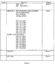
- Figure 2 is part of a computer program according to an embodiment of the present invention;
- Figure 3 is part of a computer program according to a further embodiment of the present invention;
- Figure 4 is part of a computer program according to a still further embodiment of the present invention; and
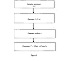
- Figure 5 is a flow diagram illustrating another embodiment of the invention.
-
- Referring to figure 2, a schematic diagram of a method for masking conditional jump statements in a computer program, according to an embodiment of the present invention, is shown generally by numeral 50. We assume that the following code fragments are executed by a processor and that a distinguishing value V varies within a known range and the condition is whether a threshold value TH is crossed by the distinguishing value V or not. The threshold TH is a random number in the known range having an upper limit and a lower limit VMAX and VMIN, respectively. In a generalized embodiment, the method comprises the steps of identifying a location for a conditional jump operation, and inserting at the location a call 52 to a subroutine 54, the subroutine 54 including instructions for changing the return address of the subroutine to one of two program branches to execute branch statements1 or branch statements2 in response to the result of a comparison of the distinguishing value V to the threshold value.
- As may be seen in figure 2, the location of the conditional jump that is replaced is identified by code block a. The subroutine is identified as IRRITATE_1 (54) and includes code blocks identified as b, c, d and e. The code block c includes a first and second sections 56 and 58, respectively. The start address of the second section 58 is predetermined and is indicated by the value KNOWN_DISPLACEMENT. The start address of the first section 56 is then determined by the difference between KNOWN_DISPLACEMENT and the upper limit of the distinguishing value V. The first section 56 consists of a series of unconditional jumps to an address L1 and the second section 58 consists of a series of unconditional jumps to an address L2. The locations L1 and L2 contain code for returning program flow to execute statements1 and statements2 respectively. The code block b included in the subroutine IRRITATE_1 includes code for computing a difference between the KNOWN_DISPLACEMENT address and the THRESHOLD. The resulting address is then added to the distinguishing value V to derive a target address location in one of the sections 56 or 58.
- As may be seen in block a the distinguishing value V is preserved while calling the subroutine, which in turn does not contain any conditional jumps. In this subroutine we change the return address of the subroutine (which resides on the stack) depending on whether V is below or above TH in such a way that, after returning from the subroutine, the program will continue execution in the desired branch.
- An addressing mode known as extended addressing is used to determine the target address. With extended addressing the address at which the execution of the program has to continue is computed as the sum of the content of two registers. For example JMP @A+DPTR in the assembly language of the Intel 8051 family means that the address at which the program execution has to continue is computed by adding the content of the accumulator A and the data pointer DPTR. Other processors may support similar mechanisms for addressing. The code fragments shown in figure 2 illustrate the method. To refer to lines of these code fragments we use labels consisting of a letter and a number. Thus to implement this method we have to specify:
- a) the address at which the block of code 56 is going to reside. That would be the address of the first JMP L1;
- b) the range of the distinguishing value V; and
- c) the maximum value of the random threshold TH. This maximum value or a value derived from it will define the size of the code block containing the JMP L1 and JMP L2 instructions.
-
- The operation of the code fragments shown in figure 2 will be discussed below. The code fragments may be located within a loop, which sequentially changes the value of V in a given range for iterations of the loop. For example V may the value of the loop counter. The goal is to continue execution at the label DO_REAL, line d1, as long as V<THRESHOLD and continue execution of instructions at the label DO_VOID , line e1, for V>= THRESHOLD.
- As mentioned earlier the THRESHOLD value is a random value within the known range of Vmin and Vmax. At line a1 the distinguishing value V is stored in the accumulator of the processor and the subroutine IRRITATE_1 is called at line a2. The return address from this subroutine will be line a3, which is automatically stored on the stack by the processor.
- The KNOWN_DISPLACEMENT in line b1 is a constant value that specifies the beginning location of the second section 58 and indicates the address of line c9. Thus KNOWN_DISPLACEMENT-Vmax is the address of line c1, the beginning location of the first section 56.
- In Block b the value of KNOWN_DISPLACEMENT is stored in a register at line b1 Next at line b2 the register is updated with the difference of KNOWN_DISPLACEMENT and THRESHOLD. This difference is moved to in DPTR at line b3. Thus, DPTR contains the address of one of the lines c1 through c8 in block c. For example for THRESHOLD = 3 DPTR would point to line c6. Assume next V and thus the contents of the accumulator can vary from 0 (Vmin) to 7 (Vmax). Then since DPTR may vary from the address of c1 to c8, the address @A+DPTR computed at line b4 can vary from the address of line c6 through c12 as V varies from 0 to7. Therefore, for V<3 the JMP L1 instructions in the first section will be executed and for V>= 3 the JMP L2 instructions in the second section will be executed.
- The labels L1 and L2 point to addresses located at lines c17 and c21 respectively. In lines c17 through c19 the return address of the subroutine IRRITATE_1 is retrieved and changed such that the program counter will point to line a3 after returning from the subroutine. In lines c21 through c23 the return address of the subroutine IRRITATE_1 is also retrieved and changed such that the program counter will point to line a4 after returning from the subroutine. The simple jump instructions at lines a3 and a4
- It may be noted that the actual distinction between the two branches to be taken is decided at lines c18 and c22 where the retrieved subroutine return address is changed to the appropriate line in block a. In the present embodiment values of 0 and 1 have been chosen since the redirection jump instructions were located immediately after the call instruction to the subroutine IRRITATE_1, at lines a3 and a4 respectively. In other implementations different values with equal number of 1's in their binary presentation may be used so that an the difference in the add operations at lines c18 and c22 is indistinguishable to an attacker. In this case an appropriate number of NOP's would be added to code block a in order to adjust the return addresses.
- Furthermore, the jump instructions in lines a3 and a4, which redirect program flow to statements1 and statements2 respectively, should be placed at addresses with the same number of 1's in their binary representation. This would result in homogenous power consumption on the address bus while addressing these two different locations. The same precaution applies to the lines d1 and e1, the beginning location of statements1 and statements2 respectively. In addition, in line b2 special attention should be paid to the choice of values of THRESHOLD and KNOWN_DISPLCEMENT to avoid changes in flags in the processors status word while the SUB instruction is being executed.
- Referring to figure 3, a second embodiment of the present invention is shown generally by numeral 100. This embodiment also utilizes extended addressing as described earlier. Again, assembly language of the Intel 8051 family of processors is used to illustrate the method. For clarity the symbols op1 through op7 are used to represent program instructions. In this embodiment, the distinguishing value V is one of two distinct values Vmax and Vmin, rather than a range of values. Thus, the condition in this case is when the distinguishing value V is one or the other of the distinct values Vmax or Vmin. Once again a call to a subroutine is inserted at a conditional jump location, the subroutine including instructions for changing the return address of the subroutine to one of two program branches to execute branch statements1 or branch statements2 in response to the distinguishing value V being one of the two distinct values Vmax or Vmin.
- As may be seen in figure 3, the location of the conditional jump that is replaced is identified by code block f. The subroutine is identified as IRRITATE_2 (102) and includes code blocks identified as blocks g and h. The code block h also includes first and second sections 106 and 108, respectively. Each of the sections contain a series of dummy operations op1 indicated at lines h1 through h7 and at lines h12 through h18. Each of the sections is terminated by a sequence of instructions for retrieving the return address of the subroutine IRRITATE_2 and changing it such that the program counter will point to line f4 or f5 after returning from the subroutine. The lines f4 and f4 include jumps to one of the two branches indicated as block i and block j which contain statements1 and statements2 respectively.
- The target destination address is comprised of two components, namely the distinguishing value V or a value derived from V and a random number MASKED_RANDOM, that are added at line g1. The beginning address of the first and second sections are chosen such that this target address is either in the range of lines h1 through h8 or h12 through h19. Since, the second component of the target address is a random number, a random number of dummy operations will be executed before the return address of the subroutine IRRITATE_2 is computed at lines h8 to h10 (or h19 to h21).
- As in the previous embodiment the ADD values at lines h9 and h20 may be chosen to have the same hamming weight(number of 1's), with appropriate number of NOP instructions added to block f. In addition the jump instructions at lines f4 and f5 may be placed at addresses with the same number of one's. Additional JMP instructions may also be inserted between the lines h1 and h8 with a destination in the same segment.
- This embodiment thus uses unconditional jumps instead of conditional jumps and adds a random number of dummy operations to the code. The former property is a countermeasure against SPA and the latter makes DPA attacks more difficult. In particular this embodiment adds a random mask or noise to the program execution path since the jump to a random address within a segment causes program execution of a random number of operations before one of the branches is executed. Therefore each time one of the branches is executed, the number of operations performed by the processor varies randomly making DPA attacks more difficult.
- In the above embodiments, a subroutine is used to redirect program flow, however in figure 4, a simple series of jumps are used. The invention is thus not restricted to the embodiments shown.
- Referring to figure 5 an embodiment of a method for masking a private key or secret used in a cryptographic operation is shown generally by numeral 200. The method comprises the steps of dividing the key into a plurality of parts and combining with each part a random value modulo n (where n is the number of points on the elliptic curve) to derive a new part such that the new parts are combined to be equivalent to the original private key value and utilizing each of the individual parts in the operation.
- As seen in figure 5, the cryptographic processor is initialized with the public key or secret value d. In computing a public key Q = dP, the secret key d is normally combined with the point P to derive dP. The value d is divided into a number of parts, eg d = b10 + b20.
- In a first step the bi's are initialized b1 = b10 and b2=b20 such that d = b10 + b20. These values of b1 and b2 are stored instead of d. Alternatively the d value may also be stored if so desired, however in the case of a smart card where memory is limited this may not be desirable.
- At a next step, a random number π is generated and the values b1 and and b2 are updated as follows:
- The updated values of b1 and b2 are stored. Computation is then performed on the point P using the components b1 and b2 as follows:
- Thus assuming the value π is randomly generated for each session then an attacker is unlikely to observe a predictable power signature.
- In a typical application of the present invention a signature component s has the form:-
- P is a point on the curve which is a predefined parameter of the system;
- k is a random integer selected as a short term private or session key;
- R = kP is the corresponding short term public key;
- a is the long term private key of the sender;
- Q = aP is the senders corresponding public key;
- e is a secure hash, such as the SHA-1 hash function, of a message m and the short term public key R; and
- n is the order of the curve.
-
- The sender sends to the recipient a message including m, s, and R and the signature is verified by computing the value R' = (sP-eQ) which should correspond to R. If the computed values correspond then the signature is verified. Both the secret keys in the above example may be masked using the method of the present invention.
Claims (15)
- A method of masking a cryptographic operation using a secret value, comprising the steps of:(a) dividing said secret value into a plurality of parts;(b) combining with each part a random value to derive a new part such that the new parts when combined are equivalent to the original secret value; and(c) utilizing each of the individual parts in said operation.
- A method as defined in claim 1, including generating a new random value at each use of said secret value.
- A method as defined in claim 1, said operation being performed in an additive group.
- A method as defined in claim 1, said operation being performed in a multiplicative group.
- A method according to claim 1 wherein said new parts are stored after each operation and said new random value is combined with said stored values for use in a subsequent operation.
- A method according to claim 1 wherein said secret value is used to generate a public key corresponding to the result of a group operation performed with said secret value, said method comprising the steps of performing said group operation on each of said parts to generate a plurality of public keys and utilizing each of said public keys in said operation.
- A method according to claim 1 wherein said cryptographic operation includes the generation of a signature component utilizing said secret value combined with additional information, said method comprising the step of combining each of said parts with said additional information and subsequently the results thereof to form said signature component.
- A method according to claim 7 wherein said results are combined with a further secret value to obtain said signature component.
- A method according to claim 8 wherein said further secret value is randomly generated for each generation of said signature component.
- An article of manufacture comprising:(a) a computer usable medium having computer readable program code embodied therein for masking a cryptographic operation using a secret value, the computer readable program code in said article of manufacture comprising;(b) computer readable program code configured to cause a computer to divide said secret value into a plurality of parts;(c) computer readable program code configured to cause a computer to combine with each part a random value to derive a new part such that the new parts when combined are equivalent to the original secret value; and(d) computer readable program code configured to cause a computer to utilize each of the individual parts in said operation.
- A method of providing a secret value d for use in a cryptographic operation comprising the steps ofi) selecting a pair of components b1, b2 that when combined correspond to said secret value, d,ii) generating a number π ,iii) combining said number π with respective ones of said components in complimentary manner to generate a pair of updated components such that a combination of said updated components is equivalent to said secret value, d, and storing said updated components.
- A method according to claim 11 wherein number π is a random number.
- A method of generating a signature component s for use in a digital signature protocol where s results from an application of a long term private key a, and a short term private key k in a signing process, said method including the steps of representing said long term private key a as a pair of components b1, b2, generating a value π, combining said value π with each of said components in a complimentary manner to generate a pair of updated components which, when combined, is equivalent to said long term key, a, performing with said updated components each of the operations normally performed by said long term private key in said signing process, combining the results of said operations to provide a value equivalent to the result of performing said operation with said long term private key, a, and utilizing said value with said private key k to provide the signature component s.
- A method according to claim 13 wherein said operations include combining said updated components with additional information.
- A method according to claim 14 wherein said additional information is derived from a message to be signed.
Applications Claiming Priority (3)
| Application Number | Priority Date | Filing Date | Title |
|---|---|---|---|
| CA002258338A CA2258338C (en) | 1999-01-11 | 1999-01-11 | Method and apparatus for minimizing differential power attacks on processors |
| CA2258338 | 1999-01-11 | ||
| EP00900195A EP1161726B1 (en) | 1999-01-11 | 2000-01-11 | Method and apparatus for minimizing differential power attacks on processors |
Related Parent Applications (1)
| Application Number | Title | Priority Date | Filing Date |
|---|---|---|---|
| EP00900195A Division EP1161726B1 (en) | 1999-01-11 | 2000-01-11 | Method and apparatus for minimizing differential power attacks on processors |
Publications (4)
| Publication Number | Publication Date |
|---|---|
| EP1365308A2 true EP1365308A2 (en) | 2003-11-26 |
| EP1365308A3 EP1365308A3 (en) | 2006-04-05 |
| EP1365308B1 EP1365308B1 (en) | 2008-12-31 |
| EP1365308B2 EP1365308B2 (en) | 2017-06-21 |
Family
ID=4163171
Family Applications (2)
| Application Number | Title | Priority Date | Filing Date |
|---|---|---|---|
| EP00900195A Expired - Lifetime EP1161726B1 (en) | 1999-01-11 | 2000-01-11 | Method and apparatus for minimizing differential power attacks on processors |
| EP03018048.3A Expired - Lifetime EP1365308B2 (en) | 1999-01-11 | 2000-01-11 | Method of masking a private key used in a cryptographic operation |
Family Applications Before (1)
| Application Number | Title | Priority Date | Filing Date |
|---|---|---|---|
| EP00900195A Expired - Lifetime EP1161726B1 (en) | 1999-01-11 | 2000-01-11 | Method and apparatus for minimizing differential power attacks on processors |
Country Status (6)
| Country | Link |
|---|---|
| EP (2) | EP1161726B1 (en) |
| JP (3) | JP5059258B2 (en) |
| AU (1) | AU1960600A (en) |
| CA (1) | CA2258338C (en) |
| DE (2) | DE60005311T2 (en) |
| WO (1) | WO2000042511A1 (en) |
Families Citing this family (18)
| Publication number | Priority date | Publication date | Assignee | Title |
|---|---|---|---|---|
| JP2001306400A (en) * | 2000-04-21 | 2001-11-02 | Sharp Corp | Semiconductor storage device, control device thereof, and electronic device |
| FR2818772A1 (en) * | 2000-12-21 | 2002-06-28 | Bull Cp8 | METHOD OF SECURING A LOGIC OR MATHEMATICAL OPERATOR IMPLANTED IN A MICROPROCESSOR ELECTRONIC MODULE, AND THE ASSOCIATED ELECTRONIC MODULE AND THE ON-LINE SYSTEM |
| JP4199937B2 (en) | 2001-03-06 | 2008-12-24 | 株式会社日立製作所 | Anti-tamper encryption method |
| FR2831739B1 (en) * | 2001-10-31 | 2005-07-22 | Gemplus Card Int | METHOD FOR SECURELY IMPLEMENTING A FUNCTIONAL MODULE IN AN ELECTRONIC COMPONENT AND CORRESPONDING COMPONENT |
| KR20040053101A (en) | 2001-11-14 | 2004-06-23 | 인터내셔널 비지네스 머신즈 코포레이션 | Device and method with reduced information leakage |
| EP1486026A1 (en) | 2002-03-07 | 2004-12-15 | Axalto SA | Method for making safe an electronic cryptography assembly with a secret key |
| DE10260801A1 (en) * | 2002-12-23 | 2004-07-08 | Infineon Technologies Ag | Execution method for a program conditional jump command, especially for use in a chip card unit, whereby the jump command causes a jump whether a condition is fulfilled or not and where there are at least two jump addresses |
| US20040162993A1 (en) * | 2003-02-13 | 2004-08-19 | Yannick Teglia | Antifraud method of an algorithm executed by an integrated circuit |
| DE10310781A1 (en) * | 2003-03-12 | 2004-09-30 | Infineon Technologies Ag | Method for operating a microprocessor and a microprocessor arrangement |
| GB2399426A (en) * | 2003-03-12 | 2004-09-15 | Sharp Kk | Fault detection in data processing apparatus |
| EP1596283B1 (en) * | 2004-05-11 | 2009-07-01 | St Microelectronics S.A. | Branch protection in a program |
| EP1899804B1 (en) | 2005-06-29 | 2012-11-07 | Irdeto B.V. | Arrangement for and method of protecting a data processing device against a cryptographic attack or analysis |
| FR2888369B1 (en) * | 2005-07-11 | 2007-10-26 | Oberthur Card Syst Sa | PROTECTION AGAINST ATTACKS BY GENERATING FAULTS ON JUMPING INSTRUCTIONS |
| DE102006014353B4 (en) * | 2006-03-28 | 2007-11-22 | Siemens Ag | Method for the reliable determination of data |
| FR2925991B1 (en) * | 2007-12-28 | 2010-01-01 | Viaccess Sa | METHOD FOR SECURING A CONDITIONAL CONNECTION, INFORMATION CARRIER, PROGRAM, SECURE SYSTEM AND SECURITY PROCESSOR FOR THIS METHOD |
| US11294633B2 (en) * | 2017-01-20 | 2022-04-05 | Nippon Telegraph And Telephone Corporation | Secure computation system, secure computation device, secure computation method, and program |
| CN111176729A (en) * | 2018-11-13 | 2020-05-19 | 深圳市中兴微电子技术有限公司 | Information processing method and device and computer readable storage medium |
| CN109493564B (en) * | 2018-11-28 | 2020-06-16 | 阿里巴巴集团控股有限公司 | Alarm method, device and system |
Family Cites Families (9)
| Publication number | Priority date | Publication date | Assignee | Title |
|---|---|---|---|---|
| US4519036A (en) * | 1983-01-05 | 1985-05-21 | Emi Limited | Program storage hardware with security scheme |
| JPH08504962A (en) * | 1992-12-22 | 1996-05-28 | テルストラ・コーポレイション・リミテッド | Encryption method |
| US5675645A (en) * | 1995-04-18 | 1997-10-07 | Ricoh Company, Ltd. | Method and apparatus for securing executable programs against copying |
| US6526456B1 (en) * | 1996-07-01 | 2003-02-25 | David Ian Allan | Distribution and controlled use of software products |
| JP3625340B2 (en) * | 1996-09-19 | 2005-03-02 | 株式会社東芝 | Security system |
| JP3440763B2 (en) * | 1996-10-25 | 2003-08-25 | 富士ゼロックス株式会社 | Encryption device, decryption device, confidential data processing device, and information processing device |
| US5991415A (en) * | 1997-05-12 | 1999-11-23 | Yeda Research And Development Co. Ltd. At The Weizmann Institute Of Science | Method and apparatus for protecting public key schemes from timing and fault attacks |
| US6804782B1 (en) * | 1999-06-11 | 2004-10-12 | General Instrument Corporation | Countermeasure to power attack and timing attack on cryptographic operations |
| JP4680876B2 (en) * | 2006-12-11 | 2011-05-11 | ルネサスエレクトロニクス株式会社 | Information processing apparatus and instruction fetch control method |
-
1999
- 1999-01-11 CA CA002258338A patent/CA2258338C/en not_active Expired - Lifetime
-
2000
- 2000-01-11 WO PCT/CA2000/000021 patent/WO2000042511A1/en not_active Ceased
- 2000-01-11 EP EP00900195A patent/EP1161726B1/en not_active Expired - Lifetime
- 2000-01-11 DE DE60005311T patent/DE60005311T2/en not_active Expired - Lifetime
- 2000-01-11 EP EP03018048.3A patent/EP1365308B2/en not_active Expired - Lifetime
- 2000-01-11 AU AU19606/00A patent/AU1960600A/en not_active Abandoned
- 2000-01-11 JP JP2000594019A patent/JP5059258B2/en not_active Expired - Lifetime
- 2000-01-11 DE DE60041285T patent/DE60041285D1/en not_active Expired - Lifetime
-
2012
- 2012-06-14 JP JP2012134710A patent/JP2012198565A/en active Pending
-
2013
- 2013-02-26 JP JP2013035344A patent/JP2013138496A/en active Pending
Non-Patent Citations (1)
| Title |
|---|
| None |
Also Published As
| Publication number | Publication date |
|---|---|
| EP1365308A3 (en) | 2006-04-05 |
| EP1365308B2 (en) | 2017-06-21 |
| EP1365308B1 (en) | 2008-12-31 |
| DE60005311D1 (en) | 2003-10-23 |
| JP5059258B2 (en) | 2012-10-24 |
| JP2012198565A (en) | 2012-10-18 |
| EP1161726A1 (en) | 2001-12-12 |
| CA2258338C (en) | 2009-02-24 |
| AU1960600A (en) | 2000-08-01 |
| CA2258338A1 (en) | 2000-07-11 |
| EP1161726B1 (en) | 2003-09-17 |
| DE60041285D1 (en) | 2009-02-12 |
| JP2013138496A (en) | 2013-07-11 |
| DE60005311T2 (en) | 2004-06-24 |
| JP2002535705A (en) | 2002-10-22 |
| WO2000042511A1 (en) | 2000-07-20 |
Similar Documents
| Publication | Publication Date | Title |
|---|---|---|
| US8660264B2 (en) | Method and apparatus for minimizing differential power attacks on processors | |
| EP1365308B2 (en) | Method of masking a private key used in a cryptographic operation | |
| US7599491B2 (en) | Method for strengthening the implementation of ECDSA against power analysis | |
| Biham et al. | Power analysis of the key scheduling of the AES candidates | |
| Messerges | Securing the AES finalists against power analysis attacks | |
| US7194633B2 (en) | Device and method with reduced information leakage | |
| US7543159B2 (en) | Device and method with reduced information leakage | |
| US20040030905A1 (en) | Encoding method and system resistant to power analysis | |
| BRPI0016507B1 (en) | method and equipment for a software provider to authenticate software users | |
| Amiel et al. | Fault analysis of DPA-resistant algorithms | |
| CA2259089C (en) | Method and apparatus for masking cryptographic operations | |
| Muir | Techniques of side channel cryptanalysis | |
| US20060023873A1 (en) | Method for secure integer division or modular reduction against hidden channel attacks | |
| EP4372548A1 (en) | Protecting cryptographic operations againt horizontal side-channel analysis attacks | |
| CA2397077A1 (en) | Encoding method and system resistant to power analysis | |
| und Computeralgebra | Hash-based Signatures on Smart Cards | |
| CA2398441A1 (en) | Method and apparatus for balanced electronic operations | |
| AU2002348963A1 (en) | Device and method with reduced information leakage |
Legal Events
| Date | Code | Title | Description |
|---|---|---|---|
| PUAI | Public reference made under article 153(3) epc to a published international application that has entered the european phase |
Free format text: ORIGINAL CODE: 0009012 |
|
| AC | Divisional application: reference to earlier application |
Ref document number: 1161726 Country of ref document: EP Kind code of ref document: P |
|
| AK | Designated contracting states |
Kind code of ref document: A2 Designated state(s): DE FR GB |
|
| PUAL | Search report despatched |
Free format text: ORIGINAL CODE: 0009013 |
|
| AK | Designated contracting states |
Kind code of ref document: A3 Designated state(s): DE FR GB |
|
| RIC1 | Information provided on ipc code assigned before grant |
Ipc: G06F 9/32 20060101ALI20060213BHEP Ipc: G06F 1/00 20060101ALI20060213BHEP Ipc: G06F 12/14 20060101AFI20060213BHEP Ipc: G06F 7/72 20060101ALI20060213BHEP |
|
| AKX | Designation fees paid | ||
| 17P | Request for examination filed |
Effective date: 20060911 |
|
| RBV | Designated contracting states (corrected) |
Designated state(s): DE FR GB |
|
| 17Q | First examination report despatched |
Effective date: 20061228 |
|
| REG | Reference to a national code |
Ref country code: DE Ref legal event code: 8566 |
|
| GRAP | Despatch of communication of intention to grant a patent |
Free format text: ORIGINAL CODE: EPIDOSNIGR1 |
|
| RIC1 | Information provided on ipc code assigned before grant |
Ipc: G06F 7/72 20060101ALI20080606BHEP Ipc: G06F 21/00 20060101AFI20080606BHEP |
|
| RTI1 | Title (correction) |
Free format text: METHOD OF MASKING A PRIVATE KEY USED IN A CRYPTOGRAPHIC OPERATION |
|
| GRAS | Grant fee paid |
Free format text: ORIGINAL CODE: EPIDOSNIGR3 |
|
| GRAA | (expected) grant |
Free format text: ORIGINAL CODE: 0009210 |
|
| AC | Divisional application: reference to earlier application |
Ref document number: 1161726 Country of ref document: EP Kind code of ref document: P |
|
| AK | Designated contracting states |
Kind code of ref document: B1 Designated state(s): DE FR GB |
|
| REG | Reference to a national code |
Ref country code: GB Ref legal event code: FG4D |
|
| REF | Corresponds to: |
Ref document number: 60041285 Country of ref document: DE Date of ref document: 20090212 Kind code of ref document: P |
|
| PLBI | Opposition filed |
Free format text: ORIGINAL CODE: 0009260 |
|
| PLAX | Notice of opposition and request to file observation + time limit sent |
Free format text: ORIGINAL CODE: EPIDOSNOBS2 |
|
| 26 | Opposition filed |
Opponent name: MUELLER, CHRISTOPH Effective date: 20090929 |
|
| PLAF | Information modified related to communication of a notice of opposition and request to file observations + time limit |
Free format text: ORIGINAL CODE: EPIDOSCOBS2 |
|
| PLBB | Reply of patent proprietor to notice(s) of opposition received |
Free format text: ORIGINAL CODE: EPIDOSNOBS3 |
|
| PLAB | Opposition data, opponent's data or that of the opponent's representative modified |
Free format text: ORIGINAL CODE: 0009299OPPO |
|
| R26 | Opposition filed (corrected) |
Opponent name: MUELLER, CHRISTOPH Effective date: 20090929 |
|
| RAP2 | Party data changed (patent owner data changed or rights of a patent transferred) |
Owner name: CERTICOM CORP. |
|
| RDAF | Communication despatched that patent is revoked |
Free format text: ORIGINAL CODE: EPIDOSNREV1 |
|
| APBM | Appeal reference recorded |
Free format text: ORIGINAL CODE: EPIDOSNREFNO |
|
| APBP | Date of receipt of notice of appeal recorded |
Free format text: ORIGINAL CODE: EPIDOSNNOA2O |
|
| APAH | Appeal reference modified |
Free format text: ORIGINAL CODE: EPIDOSCREFNO |
|
| APBQ | Date of receipt of statement of grounds of appeal recorded |
Free format text: ORIGINAL CODE: EPIDOSNNOA3O |
|
| REG | Reference to a national code |
Ref country code: FR Ref legal event code: PLFP Year of fee payment: 17 |
|
| APBU | Appeal procedure closed |
Free format text: ORIGINAL CODE: EPIDOSNNOA9O |
|
| REG | Reference to a national code |
Ref country code: FR Ref legal event code: PLFP Year of fee payment: 18 |
|
| PUAH | Patent maintained in amended form |
Free format text: ORIGINAL CODE: 0009272 |
|
| STAA | Information on the status of an ep patent application or granted ep patent |
Free format text: STATUS: PATENT MAINTAINED AS AMENDED |
|
| 27A | Patent maintained in amended form |
Effective date: 20170621 |
|
| AK | Designated contracting states |
Kind code of ref document: B2 Designated state(s): DE FR GB |
|
| REG | Reference to a national code |
Ref country code: DE Ref legal event code: R102 Ref document number: 60041285 Country of ref document: DE |
|
| REG | Reference to a national code |
Ref country code: FR Ref legal event code: PLFP Year of fee payment: 19 |
|
| PGFP | Annual fee paid to national office [announced via postgrant information from national office to epo] |
Ref country code: FR Payment date: 20190125 Year of fee payment: 20 Ref country code: DE Payment date: 20190129 Year of fee payment: 20 Ref country code: GB Payment date: 20190128 Year of fee payment: 20 |
|
| REG | Reference to a national code |
Ref country code: DE Ref legal event code: R082 Ref document number: 60041285 Country of ref document: DE Representative=s name: MERH-IP MATIAS ERNY REICHL HOFFMANN PATENTANWA, DE Ref country code: DE Ref legal event code: R081 Ref document number: 60041285 Country of ref document: DE Owner name: PITNEY BOWES, INC., STAMFORD, US Free format text: FORMER OWNER: CERTICOM CORP., MISSISSAUGA, ONTARIO, CA Ref country code: DE Ref legal event code: R081 Ref document number: 60041285 Country of ref document: DE Owner name: BLACKBERRY LIMITED, WATERLOO, CA Free format text: FORMER OWNER: CERTICOM CORP., MISSISSAUGA, ONTARIO, CA |
|
| REG | Reference to a national code |
Ref country code: DE Ref legal event code: R071 Ref document number: 60041285 Country of ref document: DE |
|
| REG | Reference to a national code |
Ref country code: GB Ref legal event code: PE20 Expiry date: 20200110 |
|
| PG25 | Lapsed in a contracting state [announced via postgrant information from national office to epo] |
Ref country code: GB Free format text: LAPSE BECAUSE OF EXPIRATION OF PROTECTION Effective date: 20200110 |
|
| REG | Reference to a national code |
Ref country code: GB Ref legal event code: 732E Free format text: REGISTERED BETWEEN 20220407 AND 20220413 |