EP1365305A1 - Enceinte anti-intrusion comprenant un maillage resistif - Google Patents
Enceinte anti-intrusion comprenant un maillage resistif Download PDFInfo
- Publication number
- EP1365305A1 EP1365305A1 EP02100484A EP02100484A EP1365305A1 EP 1365305 A1 EP1365305 A1 EP 1365305A1 EP 02100484 A EP02100484 A EP 02100484A EP 02100484 A EP02100484 A EP 02100484A EP 1365305 A1 EP1365305 A1 EP 1365305A1
- Authority
- EP
- European Patent Office
- Prior art keywords
- enclosure
- mesh
- wall
- intrusion
- conductive layers
- Prior art date
- Legal status (The legal status is an assumption and is not a legal conclusion. Google has not performed a legal analysis and makes no representation as to the accuracy of the status listed.)
- Granted
Links
Images
Classifications
-
- G—PHYSICS
- G06—COMPUTING OR CALCULATING; COUNTING
- G06F—ELECTRIC DIGITAL DATA PROCESSING
- G06F21/00—Security arrangements for protecting computers, components thereof, programs or data against unauthorised activity
- G06F21/70—Protecting specific internal or peripheral components, in which the protection of a component leads to protection of the entire computer
- G06F21/86—Secure or tamper-resistant housings
Definitions
- the present invention relates to an anti-intrusion enclosure for protect access to electronic components within the enclosure and / or data circulating between these electronic components. More in particular, the invention relates to a secure housing making it possible to detect any attempt to intrude into this box, an attempted intrusion possibly resulting in the destruction and / or the destruction out of service of electronic components within the enclosure according to the invention.
- the field of the invention is essentially that of the products of IT security, and in particular that of boxes to secure operations performed by dedicated computer servers, in particular for financial transactions.
- This type of computer server intervenes by example during purchasing operations via the Internet: when a customer wish to buy a product via the Internet, a set of procedures are put in place in which a computer server manages a set of data relating to the transaction in question, the data exchanged being most often encrypted by means of keys digital. It is essentially these keys which must be the subject of a special protection, and electronic components memorizing or allowing access to these keys are contained in secure boxes which prevent any attempt to physically access these components e.
- the enclosure anti-intrusion includes a mesh, to detect an intrusion attempt, which is directly inserted into the walls constituting the enclosure.
- These different walls are on the one hand printed circuits, preferably multilayer, and on the other hand a conductive structure composed of a flexible material comprising a set of integrated parallel conductors in this flexible material, this conductive structure commonly being called "zebra" circuit.
- one or more layers of printed circuits are used - or reserved - to arrange a set conductive tracks which will form part of the mesh of the enclosure, the conductive tracks of a printed circuit being connected to the tracks conductors of the other printed circuit via the vertical conductors of the circuit zebra.
- Holding plates are placed on the two circuits printed and come to rely on these printed circuits so as to compress the zebra circuit between the two printed circuits.
- Means of fasteners are used to maintain constant pressure on the circuit zebra thanks to the addition of these retaining plates.
- the mesh is breaks down into two main mesh elements, each element of mesh corresponding to a common thread which can consist of tracks of printed circuits and / or conductors of the zebra circuit.
- the realization such a mesh makes it possible to exploit a piezo-resistive effect of the elements constituting the mesh to detect an intrusion attempt.
- a variation resistance specific to a mesh element is detected by using example each mesh element as a resistance of a bridge of Wheatstone.
- a memory module is associated with the enclosure for memorize two initial values corresponding to the resistance value of each of the mesh elements during the commissioning of the device electronic contained in the enclosure.
- the other resistors constituting the Wheaststone bridge, as well as a device for measuring values of resistance and variation detection of these values used in such bridge mounting can be arranged in an integrated circuit preferably contained in the enclosure. So when we try for example to unscrew the holding plates, the pressure on the zebra circuit becomes less important, which results in a variation of the resistance of at least one of the elements of the mesh. A break in a track conductor or a vertical conductor constituting one of the elements of mesh obviously leads to an even greater variation in the resistance value associated with this mesh element. This variation is detected and interpreted as an attempted intrusion.
- the two mesh elements are equitably distributed over the entire surface constituting the housing according to the invention.
- the controlled technologies are thus used, which are the etching of a printed circuit, and the interconnection of conductive tracks at the by means of a zebra-type circuit, for producing an enclosure having a mesh as precise as desired, this type of realization allowing manufacture such enclosures industrially.
- the first set of layers and the second set of layers the first circuit board or second circuit board are not necessarily disjoint, that is to say that certain conductive layers can simultaneously present tracks to conduct useful signals, and ways to make a piece of the mesh.
- the mesh formed from the assembly of the first, the second and the third piece of mesh, consists of two mesh elements distinct, these two elements being intertwined throughout the walls constituting the enclosure.
- a relative variation of the resistive value of each mesh element makes it possible to determine an attempt intrusion into the housing.
- a microprocessor is arranged to inside the enclosure to use information relating to a variation relative of the resistive value of each mesh. Means of deterioration of one or more electronic components of the enclosure are provided within the enclosure, these means being used when detection of relative variation of the resistive value of each mesh greater than a predetermined threshold value, this threshold value can be stored in the memory module.
- the enclosure comprises a first retaining plate disposed on an external face of the first wall, a second retaining plate arranged on one face external of the second wall, the first and the second plate being fastened together by fastening means, for example screws and nuts so as to exert constant pressure on the three walls constituting the enclosure.
- Each element of the mesh is arranged so regular and fair on each wall of the enclosure.
- the finesse of the step of mesh must be sufficient to prevent any form of intrusion attempt, ie less than a millimeter.
- each element of the mesh is equitably arranged on each wall of the enclosure, i.e. each wall must be covered by substantially the same length of each element of mesh, no surface element of the walls having to present any significant imbalance in the distribution of the two mesh elements.
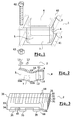
- FIG. 1 An enclosure 1 according to the invention is shown in Figure 1.
- This enclosure 1 consists of three distinct walls: a first wall 2, said upper wall, a second wall 3, called lower wall, and a third wall 4, said side wall.
- the upper wall 2 and the bottom wall 3 are two printed circuits.
- the bottom wall 3 is said opposite to the upper wall 2 insofar as no point on the wall upper 2 is in contact with the lower wall 3.
- no range access (defined later) of the upper wall 2 is not directly connected to an access area of the lower wall 3.
- each access point of the upper wall 2 cannot be in contact with an access point of the bottom wall 3 only through conductors arranged in the side wall 4.
- the wall upper 2 and the lower wall 3 are arranged in parallel, but It's not an obligation.
- Dialogue tracks allow information to be exchanged from outside the enclosure with components of the enclosure to which access is authorized.
- the side wall 4 is made of a flexible material, for example a silicone material. It constitutes a loop, the term loop designating here an approximately rectangular shape, but whose angles are rounded. Indeed, it is not possible to obtain perfectly angles rights with such material.
- the side wall 4 has a surface lateral 5, an upper surface 6 and a lower surface 7.
- the surface upper 6 is such that the upper wall 2 can come to rest on it without leaving space between the upper wall 2 and the side wall 4.
- the lower surface 7 of the side wall 4 is such that the wall lower 3 can come to rest on the side wall 4 without leaving space free between these two walls. So when the top wall 2 and the wall lower 3 are arranged on the side wall 4, the volume between these three walls, which constitutes the interior volume of enclosure 1, is perfectly closed.
- a first added plate 40 and a second added plate 41 are affixed respectively on the printed circuit constituting the wall upper 2 and on the printed circuit constituting the lower wall 3 of the enclosure.
- These plates are most often rectangular and have dimensions slightly larger than those of the upper walls and lower so that at their corners you can drill these plates without drill holes in the walls to make a device for fixing the two plates between them: this device can consist of a simple screwing performed between the two plates affixed, by means of screws 42 and nuts 43. This operation screw connection ensures compression of the side wall on the upper wall and the bottom wall so that electrical contact is made between the different tracks of the printed circuits and the vertical conductors of the side wall.
- a holding chute can be added to the upper wall 2 and / or to the lower wall 3.
- This chute helps to maintain the side wall 4. It must, at this Indeed, adopt the future outline of the side wall 4, either continuously, or only at certain points of this contour. The side wall 4 can thus come to lean on this chute, which can improve its rigidity.
- FIG. 2 is a more detailed representation of the side wall 4.
- This wall is actually a particular circuit, usually called a circuit zebra. Such a circuit is known from the state of the art. It is for example used in alphanumeric keyboards, or telephone keyboards mobile, to transmit electrical signals born from pressing on a any key on the keyboard.
- the side wall 4 has been opened in order to have a clearer view of its structure.
- This wall is made up of a flexible material, through which are arranged a set of vertical conductors 10 parallel to each other.
- These different drivers vertical can be made in different materials, which can be graphite, silver, gold ....
- a single row of conductors vertical has been shown; in other embodiments, it may however there will be more.
- Each vertical conductor 10 crosses the wall lateral in its entirety, thus making it possible to obtain, for each conductor vertical, a conduction of electrical signals between an end 11 located on the upper surface 6 and another end 12 located on the surface lower 7.
- the consecutive vertical conductors for example the vertical conductor 10A and vertical conductor 10B, are sufficiently thin to not be able to be simultaneously in contact with a first track 13 and a second access area 14 of one of the printed circuits constituting the upper wall 2 or the lower wall 3.
- a pitch 14 between two vertical conductors 10 sufficiently fine to prevent intrusion of a measuring device from outside enclosure 1 towards the interior of enclosure 1.
- Such measuring devices are intended to recover, sometimes fraudulently, electrical signals circulating between different electronic components of the enclosure, including interpretation may lead to the deduction of confidential information, and whose prohibition on access is an object of the present invention.
- the step is thus defined so that upon the intrusion of such a measuring device at across the side wall 4, this measuring device necessarily enters in contact with either of the vertical conductors 10.
- the flexible material including the vertical connectors 10 can settle slightly, unlike vertical conductors 10 which are then sufficiently exposed to come into contact with an area of appropriate contact.
- All vertical conductors of side wall 4 do not are not specific to specific access areas of printed circuits constituting the upper wall 2 or the lower wall 3, which removes a constraint in the realization of the enclosure according to the invention. Indeed, all vertical conductors having the same function, namely conducting a current between its ends 11 and 12, no matter which vertical conductor will be used to perform this function between a wall access range upper 2 and an access range of the lower wall 3.
- the tolerance in the assembly of the different walls is therefore not very restrictive. Any welding operation is obviously necessary to ensure good conduction between the different walls of the enclosure.
- Figure 3 shows a detailed representation of a wall of the enclosure, this wall possibly being the upper wall 2 or the lower wall 3.
- This wall is in fact a printed circuit 30.
- the printed circuit 30 is a multilayer circuit, that is to say that it has several conductive layers 31 isolated by layers insulators 32.
- a first set of conductive layers 33 are intended to convey useful electrical signals between different electronic components 35 of enclosure 1, and a second set of conductive layers 35 which are intended to produce part of the mesh of the enclosure according to the invention.
- the electronic components 35 can be directly arranged on the inside of the printed circuit enclosure considered, or simply be contained within the enclosure, while being however connected, possibly via other components electronic, to the first set of conductive layers 33.
- Such multilayer printed circuits exist in the state of the art and their structure will not be presented in detail in this document. It is however reminded that there may be vertical junctions, called wells conduction 46, between different conductive layers thus allowing, when necessary, to pass signals on several layers conductive.
- signals whether they are useful signals or that it is only an electrical signal circulating in the mesh, are carried on elements of conductive layers called tracks, the more often made of copper.
- tracks a set of tracks 44 of the first set of conductive layers to produce a part of the mesh of the enclosure 1.
- These tracks are symbolically represented in the form of a grid on the printed circuit 30. They stand out from useful tracks 45 used to transmit signals helpful.
- a layer conductive is intended to circulate only and exclusively useful electrical signals between components 35 or exclusively a electric current in the mesh
- a conductive layer is intended to circulate useful electrical signals and an electric current in the mesh: in other words, the first set of layers conductive 33 and the second set of conductive layers 34 are completely dissociated, that is to say certain conductive layers can belong to the first set and to the second set 33 and 34.
- each conductive track remains exclusively reserved for either an electrical signal circulating between different components 35, either to an electric current capable of flowing in the mesh.
- the first set of conductive layers 33 is not present on the wall upper or on the lower wall of the enclosure.
- the second set of conductive layers 34 which allow a protective mesh of the enclosure, is necessarily present on the wall upper 2 and on the lower wall 3 of the enclosure.
- the second set of conductive layers is arranged on the external side of the wall, i.e. on the side of the wall which will be the first exposed to an attempted intrusion into enclosure 1.
- a maximum distance ente the various conductive tracks constituting the mesh must be respected so that no signal measurement can be carried out since outside the enclosure without meeting one of these tracks. So in the invention, it is envisaged to leave a maximum pitch of approximately one millimeter between two tracks of a printed circuit intervening in the mesh.
- conduction wells not shown are arranged in the printed circuits, the end of these wells of conduction ending at the area of the printed circuit in contact with the side wall 4 by conduction pads such as the pads conduction 13 and 14 of figure 2.
- the mesh consists of three pieces, a first piece consisting of the conductive tracks reserved for the mesh of the upper wall 2, a second piece being constituted by the conductive tracks reserved for the mesh of the wall lower 3, and a third piece consisting of the conductors side wall verticals 4.
- the mesh made up of three pieces of mesh which just mentioned, is actually made up of two continuous elements not linked to each other: this means that there is a first mesh element consisting of a set of tracks on the wall upper 2, by a set of tracks of the lower wall 3 and vertical conductors 10 of the side wall 4, and a second element of grid formed by other tracks of the bottom wall 3, other tracks of the upper wall 2, and other vertical conductors of the side wall 4, so that the two mesh elements can be treated as two continuous and separate wires surrounding the interior of enclosure 1 without ever being in contact with each other.
- each element of mesh is a conductor which has a resistive value which is clean.
- each mesh element can be represented by a resistance, a variation of this resistance being detectable by means of a known type of assembly called Wheatstone bridge.
- Each of the two mesh elements constitutes one of the four resistances of this bridge, the two other resistors and the measurement circuit which can be integrated into a integrated circuit which may be one of the electronic components 35. Integration of the two mesh elements in a Wheatstone bridge allows to detect a relative variation of the resistance value of these two mesh elements.
- the resistive value of each element is measured and stored in a memory module preferably contained inside the enclosure.
- a microprocessor for example contained in the enclosure, associated with a set of applications can then make it possible to measure in permanently the resistive value of the mesh elements, and thus detect a significant variation in these resistive values.
- Such variation can be interpreted by the microprocessor as an attempt to intrude into the enclosure according to the invention, the microprocessor then being able to control the different applications for interrupting or decommissioning components placed in the enclosure according to the invention.
- the advantage of using a montage of Wheatstone bridge type is that this type of mounting allows you to measure a relative variation of the two resistive values.
- any intrusion attempt resulting in the modification of one of the resistive values of one of the mesh elements is thus detected.
- a simple intrusion attempt consists of an operation to unscrew the plates affixed to the upper and lower walls is also detected: in fact, the simple fact of unscrewing these plates leads to a decompression of the side wall 4, this decompression modifying by effect resistive piezo the resistive value of at least one of the mesh elements.
- the anti-intrusion enclosure according to the invention makes it possible to detect a attempted intrusion even when the latter does not cause breaks in a common thread constituting the mesh.
- One of the great advantages of the anti-intrusion enclosure according to the invention is to use the technologies known to make a mesh, this mesh can thus be produced from industrial way.
Landscapes
- Engineering & Computer Science (AREA)
- Computer Hardware Design (AREA)
- Theoretical Computer Science (AREA)
- General Physics & Mathematics (AREA)
- Physics & Mathematics (AREA)
- General Engineering & Computer Science (AREA)
- Software Systems (AREA)
- Computer Security & Cryptography (AREA)
- Casings For Electric Apparatus (AREA)
- Shielding Devices Or Components To Electric Or Magnetic Fields (AREA)
- Coupling Device And Connection With Printed Circuit (AREA)
- Connector Housings Or Holding Contact Members (AREA)
- Electric Double-Layer Capacitors Or The Like (AREA)
Abstract
Description
- un premier circuit imprimé multicouches constituant une première paroi de l'enceinte, pouvant comporter un premier ensemble de couches constitué d'une ou plusieurs couches conductrices, ces couches conductrices pouvant présenter des pistes conductrices nécessaires à la circulation de signaux électriques utiles entre différents composants électroniques contenus dans l'enceinte, et comportant un deuxième ensemble de couches, constitué d'une ou plusieurs couches conductrices, présentant des pistes conductrices pour réaliser un premier morceau de maillage ;
- un deuxième circuit imprimé multicouches constituant une deuxième paroi de l'enceinte opposée à la première paroi, pouvant comporter un premier ensemble de couches constitué d'une ou plusieurs couches conductrices, ces couches conductrices pouvant présenter des pistes conductrices nécessaires à la circulation de signaux électriques utiles entre différents composants électroniques contenus dans l'enceinte, et comportant un deuxième ensemble de couches, constitué d'une ou plusieurs couches conductrices, présentant des pistes conductrices pour réaliser un deuxième morceau de maillage ;
- une troisième paroi, en forme de boucle, réalisée dans une matière souple contenant un ensemble de conducteurs parallèles constituant un troisième morceau de maillage pour assurer la jonction entre des points de connexion du premier morceau de maillage et des points de connexion du deuxième morceau de maillage, la troisième paroi assurant la fermeture de l'enceinte.
- Figure 1 : une représentation schématique d'une enceinte anti-intrusion selon l'invention ;
- Figure 2 : une représentation détaillée d'un des types de paroi utilisées pour réaliser l'enceinte selon l'invention ;
- Figure 3 : une représentation détaillée d'un autre type de paroi utilisée pour la réalisation de l'enceinte selon l'invention.
Claims (13)
- Enceinte anti-intrusion (1) pour protéger un accès à des composants électroniques (35) au sein de l'enceinte (1) et/ou à des données circulant entre ces composants électroniques (35) caractérisé en ce qu'il comporte :un premier circuit imprimé multicouches constituant une première paroi (2) de l'enceinte (1), pouvant comporter un premier ensemble (33) de couches constitué d'une ou plusieurs couches conductrices, ces couches conductrices (31) pouvant présenter des pistes conductrices nécessaires à la circulation de signaux électriques utiles entre différents composants électroniques (35) contenus dans l'enceinte (1), et comportant un deuxième ensemble (34) de couches conductrices, constitué d'une ou plusieurs couches conductrices (31), présentant des pistes conductrices pour réaliser un premier morceau de maillage ;un deuxième circuit imprimé multicouches constituant une deuxième paroi (3) de l'enceinte (1) opposée à la première paroi (2), pouvant comporter un premier ensemble (33) de couches conductrices constitué d'une ou plusieurs couches conductrices (31), ces couches conductrices pouvant présenter des pistes conductrices nécessaires à la circulation de signaux électriques utiles entre différents composants électroniques (35) contenus dans l'enceinte (1), et comportant un deuxième ensemble (34) de couches conductrices, constitué d'une ou plusieurs couches conductrices(31), présentant des pistes conductrices pour réaliser un deuxième morceau de maillage ;une troisième paroi (4), en forme de boucle, réalisée dans une matière souple contenant un ensemble de conducteurs parallèles (10) constituant un troisième morceau de maillage pour assurer la jonction entre des points de connexion (13) du premier morceau de maillage et des points de connexion (11 ;12) du deuxième morceau de maillage, la troisième paroi (4) assurant la fermeture de l'enceinte (1).
- Enceinte anti-intrusion (1) selon la revendication précédente caractérisé en ce que le premier ensemble (33) de couches et le deuxième ensemble (34) de couches du premier circuit imprimé ou du deuxième circuit imprimé ne sont pas nécessairement disjoints.
- Enceinte anti-intrusion (1) selon l'une des revendications précédentes caractérisé en ce qu'il comporte une première plaque de maintien (40) disposée sur une face externe de la première paroi (2), une deuxième plaque de maintien (41) disposée sur une face externe de la deuxième paroi (3), la première et la deuxième plaque étant reliées entre elles par des moyens d'attache de façon à exercer une pression constante sur les trois parois constituant l'enceinte (1).
- Enceinte anti-intrusion (1) selon la revendication précédente caractérisé en ce que les moyens d'attache sont des vis des écrous.
- Enceinte anti-intrusion (1) selon l'une des revendications précédentes caractérisé en ce que un maillage, formé de l'assemblage du premier, du deuxième et du troisième morceau de maillage, est constitué de deux éléments de maillage distincts, ces deux éléments étant entrelacés dans l'ensemble des parois constituant l'enceinte (1).
- Enceinte anti-intrusion (1) selon la revendication 5 caractérisé en ce que chaque élément du maillage possède une valeur résistive propre qui est mémorisée dans un module de mémoire.
- Enceinte anti-intrusion (1) selon la revendication précédente caractérisé en ce que le module de mémoire est contenu dans l'enceinte (1).
- Enceinte anti-intrusion (1) selon l'une des revendications 6 ou 7 caractérisé en ce qu'il comporte un dispositif de détection d'une variation relative de la valeur résistive de chaque élément du maillage.
- Enceinte anti-intrusion (1) selon l'une des revendications 5 à 8 caractérisé en ce que chaque élément du maillage est équitablement disposé sur chaque paroi de l'enceinte (1).
- Enceinte anti-intrusion (1) selon l'une des revendications 6 à 9 caractérisé en ce qu'elle comporte un microprocesseur disposé à l'intérieur de l'enceinte (1) pour exploiter une information relative à une variation relative de la valeur résistive propre de chaque maillage.
- Enceinte anti-intrusion (1) selon l'une des revendications 6 à 10 caractérisé en ce qu'elle comporte des moyens de détérioration d'un ou plusieurs composants électroniques de l'enceinte (1), ces moyens étant mis en oeuvre lorsque lors d'une détection de variation relative de la valeur résistive propre de chaque maillage supérieure à une valeur seuil prédéterminée.
- Enceinte anti-intrusion (1) selon la revendication précédente caractérisé en ce que la valeur seuil est mémorisée dans le module de mémoire.
- Enceinte anti-intrusion (1) selon l'une des revendication précédentes caractérisé en ce que un pas du maillage est inférieur au millimètre.
Priority Applications (4)
| Application Number | Priority Date | Filing Date | Title |
|---|---|---|---|
| DE60201507T DE60201507T2 (de) | 2002-05-13 | 2002-05-13 | Eindringgeschütztes Gehäuse mit Widerstandsmaschennetzwerk |
| ES02100484T ES2227396T3 (es) | 2002-05-13 | 2002-05-13 | Recinto anti-intrusion que comprende un mallado resistivo. |
| EP02100484A EP1365305B1 (fr) | 2002-05-13 | 2002-05-13 | Enceinte anti-intrusion comprenant un maillage résistif |
| AT02100484T ATE278982T1 (de) | 2002-05-13 | 2002-05-13 | Eindringgeschütztes gehäuse mit widerstandsmaschennetzwerk |
Applications Claiming Priority (1)
| Application Number | Priority Date | Filing Date | Title |
|---|---|---|---|
| EP02100484A EP1365305B1 (fr) | 2002-05-13 | 2002-05-13 | Enceinte anti-intrusion comprenant un maillage résistif |
Publications (2)
| Publication Number | Publication Date |
|---|---|
| EP1365305A1 true EP1365305A1 (fr) | 2003-11-26 |
| EP1365305B1 EP1365305B1 (fr) | 2004-10-06 |
Family
ID=29286198
Family Applications (1)
| Application Number | Title | Priority Date | Filing Date |
|---|---|---|---|
| EP02100484A Expired - Lifetime EP1365305B1 (fr) | 2002-05-13 | 2002-05-13 | Enceinte anti-intrusion comprenant un maillage résistif |
Country Status (4)
| Country | Link |
|---|---|
| EP (1) | EP1365305B1 (fr) |
| AT (1) | ATE278982T1 (fr) |
| DE (1) | DE60201507T2 (fr) |
| ES (1) | ES2227396T3 (fr) |
Cited By (1)
| Publication number | Priority date | Publication date | Assignee | Title |
|---|---|---|---|---|
| WO2010059266A1 (fr) * | 2008-11-19 | 2010-05-27 | Sony Ericsson Mobile Communications Ab | Système et procédé de protection de cartes imprimées |
Citations (4)
| Publication number | Priority date | Publication date | Assignee | Title |
|---|---|---|---|---|
| US5060261A (en) * | 1989-07-13 | 1991-10-22 | Gemplus Card International | Microcircuit card protected against intrusion |
| EP0509567A2 (fr) * | 1991-03-28 | 1992-10-21 | Koninklijke Philips Electronics N.V. | Dispositif avec protection d'accès à de l'information protégé |
| EP0510433A2 (fr) * | 1991-04-26 | 1992-10-28 | Hughes Aircraft Company | Structure de circuit sûr |
| US20020002683A1 (en) * | 2000-02-14 | 2002-01-03 | Benson Justin H. | Security module system, apparatus and process |
-
2002
- 2002-05-13 DE DE60201507T patent/DE60201507T2/de not_active Expired - Lifetime
- 2002-05-13 ES ES02100484T patent/ES2227396T3/es not_active Expired - Lifetime
- 2002-05-13 EP EP02100484A patent/EP1365305B1/fr not_active Expired - Lifetime
- 2002-05-13 AT AT02100484T patent/ATE278982T1/de not_active IP Right Cessation
Patent Citations (4)
| Publication number | Priority date | Publication date | Assignee | Title |
|---|---|---|---|---|
| US5060261A (en) * | 1989-07-13 | 1991-10-22 | Gemplus Card International | Microcircuit card protected against intrusion |
| EP0509567A2 (fr) * | 1991-03-28 | 1992-10-21 | Koninklijke Philips Electronics N.V. | Dispositif avec protection d'accès à de l'information protégé |
| EP0510433A2 (fr) * | 1991-04-26 | 1992-10-28 | Hughes Aircraft Company | Structure de circuit sûr |
| US20020002683A1 (en) * | 2000-02-14 | 2002-01-03 | Benson Justin H. | Security module system, apparatus and process |
Non-Patent Citations (1)
| Title |
|---|
| WEINGART S H: "PHYSICAL SECURITY DEVICES FOR COMPUTER SUBSYSTEMS: A SURVEY OF ATTACKS AND DEFENSES", CRYPTOGRAPHIC HARDWARE AND EMBEDDED SYSTEMS. 2ND INTERNATIONAL WORKSHOP, CHES 2000, WORCHESTER, MA, AUG. 17 - 18, 2000 PROCEEDINGS, LECTURE NOTES IN COMPUTER SCIENCE, BERLIN: SPRINGER, DE, vol. 1965, 17 August 2000 (2000-08-17), pages 302 - 317, XP001049140, ISBN: 3-540-41455-X * |
Cited By (1)
| Publication number | Priority date | Publication date | Assignee | Title |
|---|---|---|---|---|
| WO2010059266A1 (fr) * | 2008-11-19 | 2010-05-27 | Sony Ericsson Mobile Communications Ab | Système et procédé de protection de cartes imprimées |
Also Published As
| Publication number | Publication date |
|---|---|
| ATE278982T1 (de) | 2004-10-15 |
| DE60201507D1 (de) | 2004-11-11 |
| DE60201507T2 (de) | 2005-10-20 |
| EP1365305B1 (fr) | 2004-10-06 |
| ES2227396T3 (es) | 2005-04-01 |
Similar Documents
| Publication | Publication Date | Title |
|---|---|---|
| FR2888975A1 (fr) | Procede de securisation pour la protection de donnees | |
| CA2654060C (fr) | Dispositif de protection contre les intrusions d'appareils electroniques | |
| EP2866259B1 (fr) | Puce électronique comprenant des moyens de protection de sa face arrière | |
| EP2076862A1 (fr) | Dispositif de protection pour carte electronique | |
| EP1126358B1 (fr) | Dispositif anti-intrusion | |
| WO2005069210A1 (fr) | Protection d'une puce de circuit integre contenant des donnees confidentielles | |
| WO2010058094A1 (fr) | Dispositif de protection d'un boitier de circuit intégré électronique contre les intrusions par voie physique ou chimique | |
| FR2971366A1 (fr) | Micro plaquette de semi-conducteur comprenant des moyens de protection contre une attaque physique | |
| FR2985153A1 (fr) | Dispositif de protection d'un circuit imprime electronique. | |
| EP2241997B1 (fr) | Lecteur de carte mémoire | |
| EP0776498B1 (fr) | Dispositif de clavier securise | |
| EP1365305B1 (fr) | Enceinte anti-intrusion comprenant un maillage résistif | |
| CN101803018A (zh) | 安全芯片 | |
| EP1671341B1 (fr) | Dispositif anti-intrusion notamment pour terminal de paiement electronique | |
| EP1053531B1 (fr) | Dispositif a circuit integre securise par attenuation de signatures electriques | |
| EP2102832B1 (fr) | Boitier securise | |
| FR2857113A1 (fr) | Boitier securise renfermant un clavier permettant d'introduire des donnees confidentielles | |
| EP1400887A1 (fr) | Dispositif de protection pour puce électronique comportant des informations confidentielles | |
| EP3107358A1 (fr) | Composant de protection de signaux sensibles, dispositif et procédé correspondant | |
| EP3295365A1 (fr) | Détection d'ouverture d'un dispositif de saisie de données | |
| FR2910708A1 (fr) | Protection de donnees confidentielles dans les circuits integres | |
| FR2892544A1 (fr) | Detection de tentative d'effraction sur une puce a travers sa structure support | |
| FR2985338A1 (fr) | Clavier securise |
Legal Events
| Date | Code | Title | Description |
|---|---|---|---|
| PUAI | Public reference made under article 153(3) epc to a published international application that has entered the european phase |
Free format text: ORIGINAL CODE: 0009012 |
|
| AK | Designated contracting states |
Kind code of ref document: A1 Designated state(s): AT BE CH CY DE DK ES FI FR GB GR IE IT LI LU MC NL PT SE TR |
|
| AX | Request for extension of the european patent |
Extension state: AL LT LV MK RO SI |
|
| GRAP | Despatch of communication of intention to grant a patent |
Free format text: ORIGINAL CODE: EPIDOSNIGR1 |
|
| 17P | Request for examination filed |
Effective date: 20040206 |
|
| RIN1 | Information on inventor provided before grant (corrected) |
Inventor name: DUMONT, DENIS |
|
| GRAS | Grant fee paid |
Free format text: ORIGINAL CODE: EPIDOSNIGR3 |
|
| AKX | Designation fees paid |
Designated state(s): AT BE CH CY DE DK ES FI FR GB GR IE IT LI LU MC NL PT SE TR |
|
| GRAA | (expected) grant |
Free format text: ORIGINAL CODE: 0009210 |
|
| AK | Designated contracting states |
Kind code of ref document: B1 Designated state(s): AT BE CH CY DE DK ES FI FR GB GR IE IT LI LU MC NL PT SE TR |
|
| PG25 | Lapsed in a contracting state [announced via postgrant information from national office to epo] |
Ref country code: AT Free format text: LAPSE BECAUSE OF FAILURE TO SUBMIT A TRANSLATION OF THE DESCRIPTION OR TO PAY THE FEE WITHIN THE PRESCRIBED TIME-LIMIT Effective date: 20041006 Ref country code: TR Free format text: LAPSE BECAUSE OF FAILURE TO SUBMIT A TRANSLATION OF THE DESCRIPTION OR TO PAY THE FEE WITHIN THE PRESCRIBED TIME-LIMIT Effective date: 20041006 Ref country code: IE Free format text: LAPSE BECAUSE OF FAILURE TO SUBMIT A TRANSLATION OF THE DESCRIPTION OR TO PAY THE FEE WITHIN THE PRESCRIBED TIME-LIMIT Effective date: 20041006 Ref country code: FI Free format text: LAPSE BECAUSE OF FAILURE TO SUBMIT A TRANSLATION OF THE DESCRIPTION OR TO PAY THE FEE WITHIN THE PRESCRIBED TIME-LIMIT Effective date: 20041006 Ref country code: NL Free format text: LAPSE BECAUSE OF FAILURE TO SUBMIT A TRANSLATION OF THE DESCRIPTION OR TO PAY THE FEE WITHIN THE PRESCRIBED TIME-LIMIT Effective date: 20041006 |
|
| REG | Reference to a national code |
Ref country code: GB Ref legal event code: FG4D Free format text: NOT ENGLISH |
|
| REG | Reference to a national code |
Ref country code: CH Ref legal event code: EP |
|
| REG | Reference to a national code |
Ref country code: IE Ref legal event code: FG4D Free format text: FRENCH |
|
| REF | Corresponds to: |
Ref document number: 60201507 Country of ref document: DE Date of ref document: 20041111 Kind code of ref document: P |
|
| GBT | Gb: translation of ep patent filed (gb section 77(6)(a)/1977) |
Effective date: 20041202 |
|
| PG25 | Lapsed in a contracting state [announced via postgrant information from national office to epo] |
Ref country code: GR Free format text: LAPSE BECAUSE OF FAILURE TO SUBMIT A TRANSLATION OF THE DESCRIPTION OR TO PAY THE FEE WITHIN THE PRESCRIBED TIME-LIMIT Effective date: 20050106 Ref country code: DK Free format text: LAPSE BECAUSE OF FAILURE TO SUBMIT A TRANSLATION OF THE DESCRIPTION OR TO PAY THE FEE WITHIN THE PRESCRIBED TIME-LIMIT Effective date: 20050106 |
|
| NLV1 | Nl: lapsed or annulled due to failure to fulfill the requirements of art. 29p and 29m of the patents act | ||
| REG | Reference to a national code |
Ref country code: ES Ref legal event code: FG2A Ref document number: 2227396 Country of ref document: ES Kind code of ref document: T3 |
|
| PG25 | Lapsed in a contracting state [announced via postgrant information from national office to epo] |
Ref country code: LU Free format text: LAPSE BECAUSE OF NON-PAYMENT OF DUE FEES Effective date: 20050513 Ref country code: CY Free format text: LAPSE BECAUSE OF FAILURE TO SUBMIT A TRANSLATION OF THE DESCRIPTION OR TO PAY THE FEE WITHIN THE PRESCRIBED TIME-LIMIT Effective date: 20050513 |
|
| REG | Reference to a national code |
Ref country code: IE Ref legal event code: FD4D |
|
| PG25 | Lapsed in a contracting state [announced via postgrant information from national office to epo] |
Ref country code: BE Free format text: LAPSE BECAUSE OF NON-PAYMENT OF DUE FEES Effective date: 20050531 Ref country code: MC Free format text: LAPSE BECAUSE OF NON-PAYMENT OF DUE FEES Effective date: 20050531 |
|
| PLBE | No opposition filed within time limit |
Free format text: ORIGINAL CODE: 0009261 |
|
| STAA | Information on the status of an ep patent application or granted ep patent |
Free format text: STATUS: NO OPPOSITION FILED WITHIN TIME LIMIT |
|
| 26N | No opposition filed |
Effective date: 20050707 |
|
| BERE | Be: lapsed |
Owner name: SAGEM S.A. Effective date: 20050531 |
|
| REG | Reference to a national code |
Ref country code: FR Ref legal event code: TP |
|
| PG25 | Lapsed in a contracting state [announced via postgrant information from national office to epo] |
Ref country code: LI Free format text: LAPSE BECAUSE OF NON-PAYMENT OF DUE FEES Effective date: 20060531 Ref country code: CH Free format text: LAPSE BECAUSE OF NON-PAYMENT OF DUE FEES Effective date: 20060531 |
|
| REG | Reference to a national code |
Ref country code: CH Ref legal event code: PL |
|
| BERE | Be: lapsed |
Owner name: S.A. *SAGEM Effective date: 20050531 |
|
| PG25 | Lapsed in a contracting state [announced via postgrant information from national office to epo] |
Ref country code: PT Free format text: LAPSE BECAUSE OF NON-PAYMENT OF DUE FEES Effective date: 20050306 |
|
| PGFP | Annual fee paid to national office [announced via postgrant information from national office to epo] |
Ref country code: FR Payment date: 20070529 Year of fee payment: 6 |
|
| REG | Reference to a national code |
Ref country code: FR Ref legal event code: TP |
|
| REG | Reference to a national code |
Ref country code: GB Ref legal event code: 732E |
|
| REG | Reference to a national code |
Ref country code: FR Ref legal event code: ST Effective date: 20090119 |
|
| PG25 | Lapsed in a contracting state [announced via postgrant information from national office to epo] |
Ref country code: FR Free format text: LAPSE BECAUSE OF NON-PAYMENT OF DUE FEES Effective date: 20080602 |
|
| REG | Reference to a national code |
Ref country code: DE Ref legal event code: R082 Ref document number: 60201507 Country of ref document: DE Representative=s name: J D REYNOLDS & CO., GB Effective date: 20120308 Ref country code: DE Ref legal event code: R081 Ref document number: 60201507 Country of ref document: DE Owner name: MORPHO, FR Free format text: FORMER OWNER: SAGEM SECURITE, PARIS, FR Effective date: 20120308 |
|
| REG | Reference to a national code |
Ref country code: DE Ref legal event code: R082 Ref document number: 60201507 Country of ref document: DE Representative=s name: J D REYNOLDS & CO., GB |
|
| PGFP | Annual fee paid to national office [announced via postgrant information from national office to epo] |
Ref country code: ES Payment date: 20120508 Year of fee payment: 11 |
|
| PGFP | Annual fee paid to national office [announced via postgrant information from national office to epo] |
Ref country code: SE Payment date: 20130425 Year of fee payment: 12 |
|
| PGFP | Annual fee paid to national office [announced via postgrant information from national office to epo] |
Ref country code: IT Payment date: 20130424 Year of fee payment: 12 |
|
| PG25 | Lapsed in a contracting state [announced via postgrant information from national office to epo] |
Ref country code: SE Free format text: LAPSE BECAUSE OF NON-PAYMENT OF DUE FEES Effective date: 20140514 |
|
| REG | Reference to a national code |
Ref country code: SE Ref legal event code: EUG |
|
| PG25 | Lapsed in a contracting state [announced via postgrant information from national office to epo] |
Ref country code: IT Free format text: LAPSE BECAUSE OF NON-PAYMENT OF DUE FEES Effective date: 20140513 |
|
| REG | Reference to a national code |
Ref country code: ES Ref legal event code: FD2A Effective date: 20150630 |
|
| PG25 | Lapsed in a contracting state [announced via postgrant information from national office to epo] |
Ref country code: ES Free format text: LAPSE BECAUSE OF NON-PAYMENT OF DUE FEES Effective date: 20140514 |
|
| PGFP | Annual fee paid to national office [announced via postgrant information from national office to epo] |
Ref country code: DE Payment date: 20150422 Year of fee payment: 14 Ref country code: GB Payment date: 20150424 Year of fee payment: 14 |
|
| REG | Reference to a national code |
Ref country code: DE Ref legal event code: R119 Ref document number: 60201507 Country of ref document: DE |
|
| GBPC | Gb: european patent ceased through non-payment of renewal fee |
Effective date: 20160513 |
|
| PG25 | Lapsed in a contracting state [announced via postgrant information from national office to epo] |
Ref country code: DE Free format text: LAPSE BECAUSE OF NON-PAYMENT OF DUE FEES Effective date: 20161201 |
|
| PG25 | Lapsed in a contracting state [announced via postgrant information from national office to epo] |
Ref country code: GB Free format text: LAPSE BECAUSE OF NON-PAYMENT OF DUE FEES Effective date: 20160513 |